

Datasheet 74ACQ241SCX, 74ACQ241SC, 74ACQ241PC, 74ACQ241MSA, 74ACQ241CW Datasheet (Fairchild Semiconductor)
Page 1
January 1990
Revised September 1998
74ACQ241 Octal Buffer/Line Driver with 3-STATE Outputs
© 1998 Fairchild Semiconductor Corporation DS010642.prf www.fairchildsemi.com
74ACQ241
Octal Buffer/Line Driver with 3-STATE Outputs
General Description
The ACQ241 is an oct al buffer and line drive r designed to
be employed as a m em ory add re ss dr i ver, clock driver a nd
bus oriented transmitter or receiver which provides
improved PC board density. The ACQ utilizes Fairchild
FACT Quiet Series technology to guarantee quiet output
switching and improved dynamic threshold performance.
FACT Quiet Series features GTO output control and
undershoot corr ector in addition to a split ground bus for
superior performance.
Features
■ ICC and IOZ reduced by 50%
■ Guaranteed simultaneous switching noise level and
dynamic threshold performance
■ Guaranteed pin-to-pin skew AC performance
■ Improved latch-up immunity
■ 3-STATE outputs drive bus lines or buffer memory
address registers
■ Outputs source/sink 24 mA
■ Faster prop delays than the standard AC
Ordering Code:
Device also available in Tape and Reel. Specify by appending suffix letter “X” to the ordering co de.
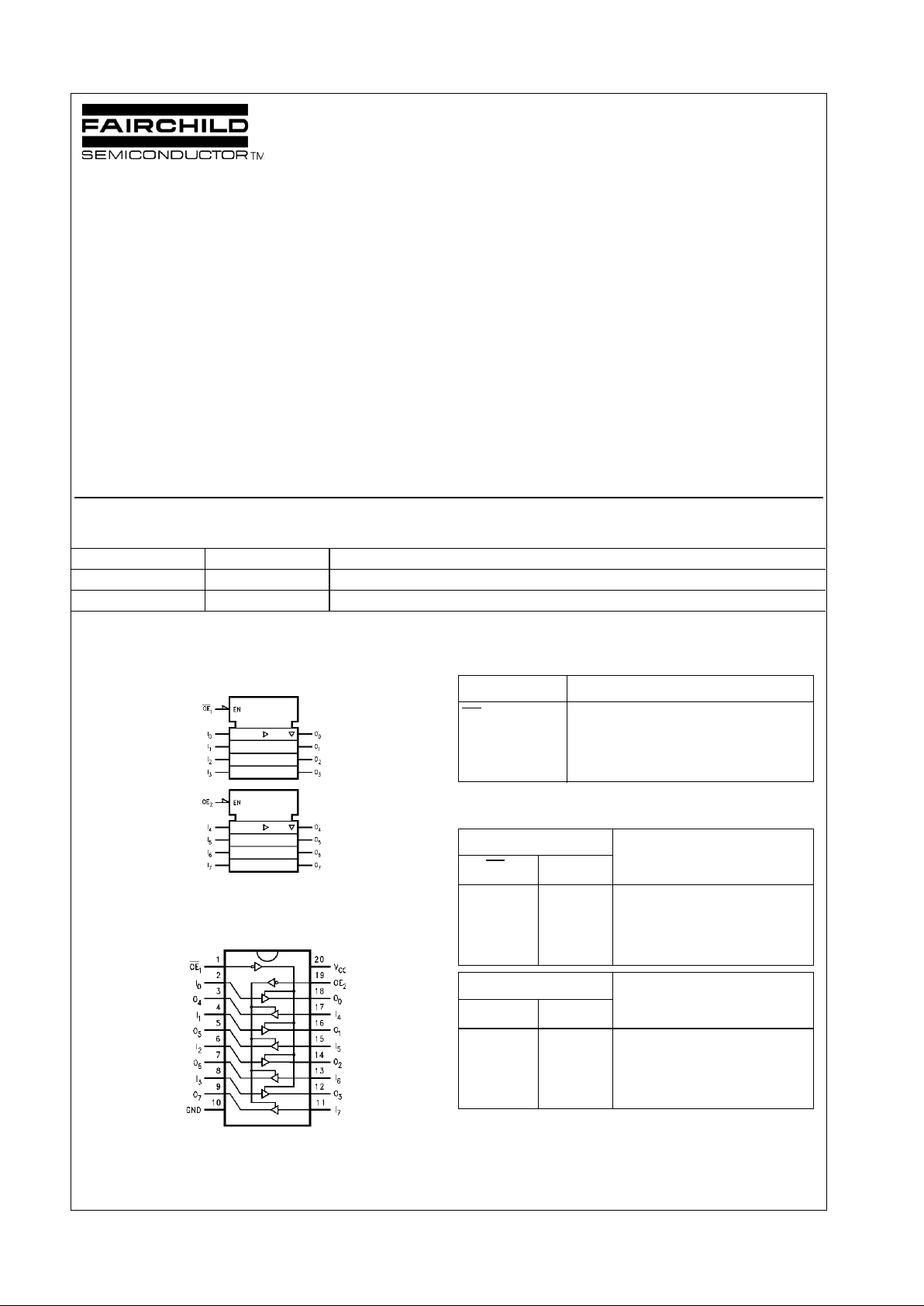
Logic Symbol
IEEE/IEC
Connection Diagram
Pin Assignme nt for DIP and SOIC
Pin Descriptions
Truth Tables
H = HIGH Voltage Level X = Immaterial
L = LOW Voltage Level Z = High Impedance
FACT, FACT Quiet Series, a nd GTO are trademarks of F airchild Semicond uc t or Corporation .
Order Number Package Number Package Description
74ACQ241SC M20B 20-Lead Small Outline Integrated Circuit, JEDEC MS-013, 0.300” Wide Body
74ACQ241PC N20A 20-Lead Plastic Dual-In-Line Package, JEDEC MS-001, 0.300” Wide
Pin Names Description
OE
1
, OE
2
3-STATE Output Enable Inputs
I
0–I7
Inputs
O
0–O7
Outputs
Inputs Outputs
OE
1
I
n
(Pins 12, 14, 16, 18)
LL L
LH H
HX Z
Inputs Outputs
OE
2
I
n
(Pins 3, 5, 7, 9)
HL L
HH H
HX Z
Page 2

www.fairchildsemi.com 2
74ACQ241
Absolute Maximum Ratings(Note 1) Recommended Operating
Conditions
Note 1: Absolute maximum ratings are those values beyond which damage
to the device may occur. The databook specifications should be met, without exception, to ensure that the system design is reliable over its po wer
supply, temperature, and output /input lo ading variable s. Fairch ild do es not
recommend operation of FACT circuits out s ide databook specifications.
Supply Voltage (VCC) −0.5V to +7.0V
DC Input Diode Current (I
IK
)
V
I
= −0.5V −20 mA
V
I
= VCC + 0.5V +20 mA
DC Input Voltage (V
I
) −0.5V to VCC + 0.5V
DC Output Diode Current (I
OK
)
V
O
= −0.5V −20 mA
V
O
= VCC + 0.5V +20 mA
DC Output Voltage (V
O
) −0.5V to VCC + 0.5V
DC Output Source
or Sink Current (I
O
) ± 50 mA
DC V
CC
or Ground Current
per Output Pin (I
CC
or I
GND
) ± 50 mA
Storage Temperature (T
STG
) −65°C to +150°C
DC Latch-Up Source or
Sink Current ±300 mA
Junction Temperature (T
J
)
PDIP 140°C
Supply Voltage (V
CC
) 2.0V to 6.0V
Input Voltage (V
I
) 0V to V
CC
Output Voltage (VO) 0V to V
CC
Operating Temperature (TA) −40°C to +85°C
Minimum Input Edge Rate ∆V/∆t 125 mV/ns
V
IN
from 30% to 70% of V
CC
VCC @ 3.0V, 4.5V, 5.5V
Page 3
3 www.fairchildsemi.com
74ACQ241
DC Electrical Characteristics
Note 2: All outputs loaded; thresholds on input assoc iated with outpu t un der test.
Note 3: Maximum test duration 2.0 ms, one output loaded at a time.
Note 4: I
IN
and ICC @ 3.0V are guar ant eed to be less tha n or equal to the respe ctiv e limit @ 5.5V VCC.
Note 5: DIP packa ge.
Note 6: Max number of outputs defined as (n). Data Inputs are driven 0V to 5V. One output @ GND.
Note 7: Max number of Data Inputs (n) switching. n−1 Inputs s w it c hing 0V to 5V . Input- under-test switch ing: 5V to threshol d (V
ILD
), 0V to threshold (V
IHD
),
f = 1 MHz.
Symbol Parameter V
CC
TA = +25°CT
A
= −40°C to +85°C Units Conditions
(V) Typ Guaranteed Limits
V
IH
Minimum High Level 3.0 1.5 2.1 2.1 V
OUT
= 0.1V
Input Voltage 4.5 2.25 3.15 3.15 V or VCC − 0.1V
5.5 2.75 3.85 3.85
V
IL
Maximum Low Level 3.0 1.5 0.9 0.9 V
OUT
= 0.1V
Input Voltage 4.5 2.25 1.35 1.35 V or VCC − 0.1V
5.5 2.75 1.65 1.65
V
OH
Minimum High Level 3.0 2.99 2.9 2.9 I
OUT
= −50 µA
Output Voltage 4.5 4.49 4.4 4.4 V
5.5 5.49 5.4 5.4
VIN = VIL or V
IH
3.0 2.56 2.46
V
IOH = −12 mA
4.5 3.86 3.76 IOH = −24 mA
5.5 4.86 4.76 IOH = −24 mA (Note 2)
V
OL
Maximum Low Level 3.0 0.002 0.1 0.1 I
OUT
= 50 µA
Output Voltage 4.5 0.001 0.1 0.1 V
5.5 0.001 0.1 0.1
VIN = VIL or V
IH
3.0 0.36 0.44 IOL = 12 mA
4.5 0.36 0.44 V IOL = 24 mA
5.5 0.36 0.44 IOL = 24 mA (Note 2)
I
IN
(Note 4)
Maximum Input Leakage Current
5.5 ± 0.1 ± 1.0 µA
VI = VCC, GND
I
OLD
Minimum Dynamic
Output Current
5.5 75 mA V
OLD
= 1.65V Max
I
OHD
(Note 3) 5.5 −75 mA V
OHD
= 3.85V Min
I
CC
(Note 4)
Maximum Quiescent
Supply Current
5.5 4.0 40.0 µA
VIN = VCC or GND
I
OZ
Maximum 3-STATE 5.5 ±0.25 ±2.5 µAVI (OE) = VIL, V
IH
Leakage Current VI = VCC, GND
VO = VCC, GND
V
OLP
Quiet Output 5.0 1.1 1.5 V Figures 1, 2
Maximum Dynamic V
OL
(Note 5)(Note 6)
V
OLV
Quiet Output 5.0 −0.6 −1.2 V Figures 1, 2
Minimum Dynamic V
OL
(Note 5)(Note 6)
V
IHD
Minimum High Level 5.0 3.1 3.5 V (Note 5)(Note 7)
Dynamic Input Voltage
V
ILD
Maximum Low Level 5.0 1.9 1.5 V (Note 5)(Note 7)
Dynamic Input Voltage
Page 4

www.fairchildsemi.com 4
74ACQ241
AC Electrical Characteristics
Note 8: Voltage Range 5. 0 is 5. 0V ±0.5V. Voltage Range 3.3 is 3.3V ±0.3V.
Note 9: Skew is defin ed as the absolute value of the difference bet w een the actual p ropagation delay for any two s eparate outpu ts of the same devic e. The
specification applies to any out puts switching in th e s am e direction, eith er H I GH to LOW (t
OSHL
) or LOW to HIGH (t
OSLH
). Parameter guaranteed by design.
Capacitance
Symbol Parameter V
CC
TA = +25°CT
A
= −40°C to +85°CUnits
(V) CL = 50 pF CL = 50 pF
(Note 8) Min Typ Max Min Max
t
PHL
Propagation Delay 3.3 2.0 6.5 9.0 2.0 9.5 ns
t
PLH
Data to Output 5.0 1.5 4.5 6.0 1.5 6.5
t
PZL
Output Enable Time 3.3 2.5 8.0 13.0 2.5 13.5 ns
t
PZH
5.0 1.5 5.5 8.5 1.5 9.0
t
PHZ
Output Disable Time 3.3 1.0 8.5 14.5 1.0 15.0 ns
t
PLZ
5.0 1.0 5.5 9.5 1.0 10.0
t
OSHL
t
OSLH
Output to Output
Skew Data to Output (Note 9)
3.3 1.0 1.5 1.5 ns
Symbol Parameter Typ Units Conditions
C
IN
Input Capacitance 4.5 pF VCC = OPEN
C
PD
Power Dissipation Capacitance 70 pF VCC = 5.0V
Page 5

5 www.fairchildsemi.com
74ACQ241
FACT Noise Characteristics
The setup of a noise characteristics measurement is critical
to the accuracy and repeatability of the tests. The following
is a brief description of the setup used to measure the
noise characteristics of FACT.
Equipment:
Hewlett Packard Model 8180A Word Generator
PC-163A Test Fixture
Tektronics Model 7854 Oscilloscope
Procedure:
1. Verify Test Fixture Loading: Standard Load 50 pF,
500Ω.
2. Deskew the HFS generator so that no two channels
have greater than 150 ps skew between them. This
requires that the oscilloscope be deskewe d first. It is
important to deskew the HFS generator channels
before testing. This will ensure that the outputs switch
simultaneously.
3. Terminate all inputs and outputs to ensure proper loading of the outputs and that the input levels are at the
correct voltage.
4. Set the HFS generator to toggl e all but on e outpu t at a
frequency of 1 MHz. Greater frequencies will increase
DUT heating and effect the results of the measurement.
5. Set the word genera tor input l evels at 0V LOW and 3V
HIGH for ACT devices and 0V LOW and 5V HIGH for
AC devices. Verify levels with an oscilloscope
FIGURE 1. Quiet Output Noise Voltage Waveforms
Note 10: V
OHV
and V
OLP
are measured wi th r es pect to ground reference.
Note 11: Input pulses have the following characte ristics: f = 1 MHz, t
r
=
3 ns, t
f
= 3 ns, skew < 150ps.
V
OLP/VOLV
and V
OHP/VOHV
:
• Determine the quiet output pin that demonstrates the
greatest noise levels . The worst case pin will usually be
the furthest from th e g rou nd pin . Mo ni to r t he out put vol tages using a 50Ω coaxi al cable plug ged into a stand ard
SMB type connector on the test fixture. Do not use an
active FET probe.
• Measure V
OLP
and V
OLV
on the quiet outpu t during the
worst case transition for active and enable. Measure
V
OHP
and V
OHV
on the quiet output during the worst
case active and enable transition.
• Verify that the GND reference recorded on the oscilloscope has not drifted to ensure the accuracy and repeatability of the measurements.
V
ILD
and V
IHD
:
• Monitor one of the switching outputs using a 50Ω coaxial
cable plugged i nto a standard SMB type conne ctor on
the test fixture. Do not use an active FET probe.
• First increase the input LOW voltage level, V
IL
, until the
output begins to oscillate or steps out a min of 2 ns.
Oscillation is defined as noise on the output LOW level
that exceeds V
IL
limits, or on output HIGH levels that
exceed V
IH
limits. The input LOW voltage level at which
oscillation occurs is defined as V
ILD
.
• Next decrease the input HIGH voltage level, V
IH
, until
the output begin s to osc illate or step s out a mi n of 2 ns.
Oscillation is defined as noise on the output LOW level
that exceeds V
IL
limits, or on output HIGH levels that
exceed V
IH
limits. The input HIGH voltage level at which
oscillation occurs is defined as V
IHD
.
• Verify that the GND reference recorded on the oscilloscope has not drifted to ensure the accuracy and repeatability of the measurements.
FIGURE 2. Simultaneous Switching Test Circuit
Page 6

www.fairchildsemi.com 6
74ACQ241
Physical Dimensions inches (millimeters) unless otherwise noted
20-Lead Small Outline Integrated Circuit, JEDEC MS-013, 0.300” Wide Body
Package Number M20B
Page 7

Fairchild does not assume any responsibility for use of any circuitry described, no circuit patent licenses are implied and Fairchild reserves the right at any time without notice to change said circuitry and specifications.
74ACQ241 Octal Buffer/Line Driver with 3-STATE Outputs
LIFE SUPPORT POLICY
FAIRCHILD’S PRODUCTS ARE NOT AUTHORIZED FOR USE AS CRITICAL COMPONENTS IN LIFE SUPPORT
DEVICES OR SYSTEMS WITHOUT THE EXPRESS WRITTEN APPROVAL OF THE PRESIDENT OF FAIRCHILD
SEMICONDUCTOR CORPORATION. As used herein:
1. Life support devices or syst ems are devices or systems
which, (a) are intended for surgical implant into the
body, or (b) support or sustain life, and (c) whose failure
to perform when properly used in accordance with
instructions for use pr ovide d in the labeling, can be reasonably expected to resu lt in a significant injury to t he
user.
2. A critical com ponent i n any compo nent o f a life s upp ort
device or system whose failure to perform ca n be reasonably expected to cause the failure of the l ife s upp or t
device or system, or to affect its safety or effectiveness.
www.fairchildsemi.com
Physical Dimensions in ches (millimeters) unless otherwise noted (Continued)
20-Lead Plastic Dual-In-Line Package, JEDEC MS-001, 0.300” Wide
Package Number N20A
 Loading...