

Page 1
© 2000 Fairchild Semiconductor Corporation DS010133 www.fairchildsemi.com
November 1988
Revised August 2000
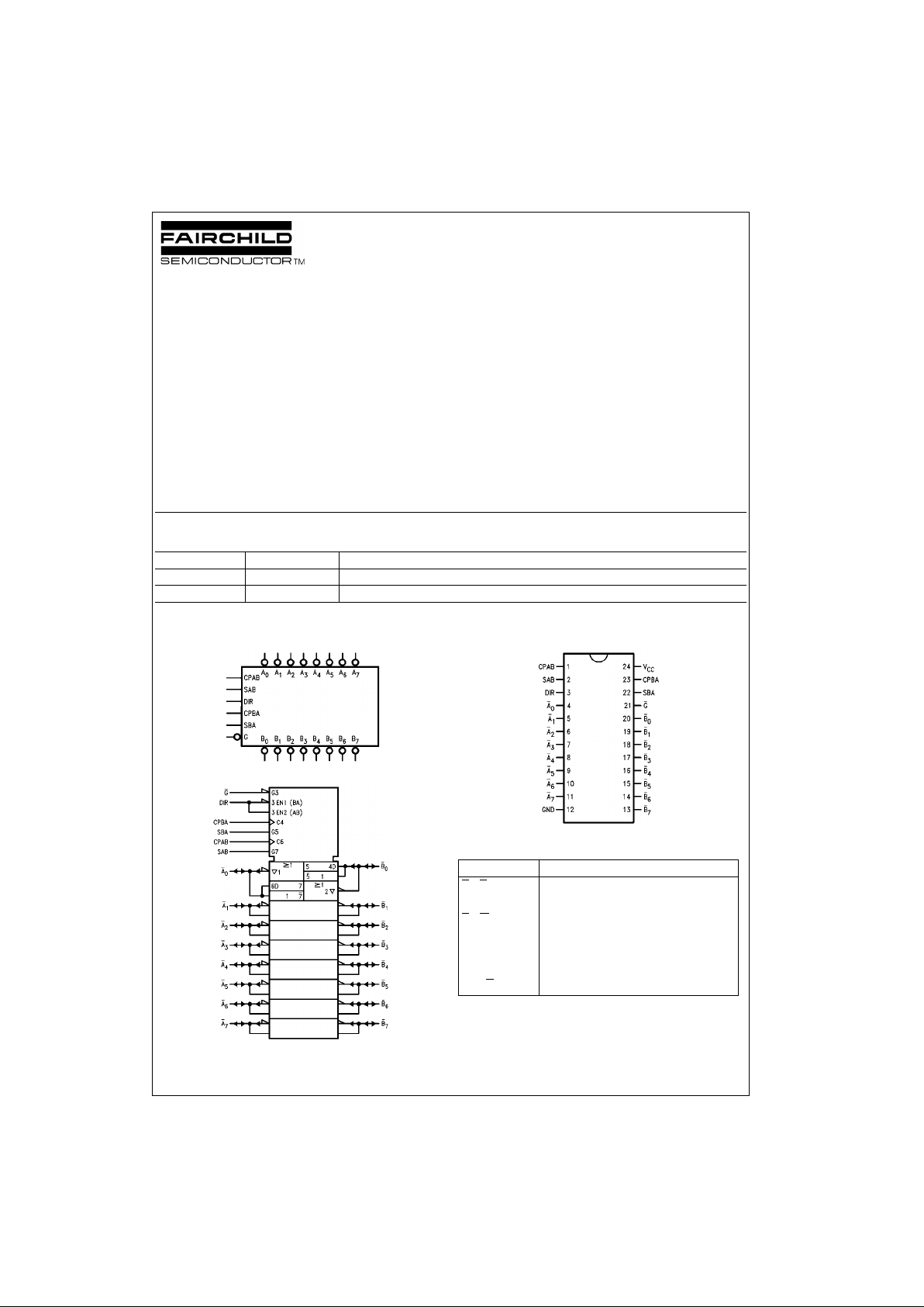
74AC648 Octal Transceiver/Register with 3-STATE Outputs
74AC648
Octal Transceiver/Register with 3-STATE Outputs
General Description
The AC648 consists of register ed bus transceiver circ uits,
with outputs, D-type flip-flops and control circuitry providing
multiplexed transmission of da ta directly from the input bus
or from the interna l storage registers . Data on the A or B
bus will be loaded into the respective registers on the
LOW-to-HIGH transition of the appropriate clock pin (CPAB
or CPBA). The four fundamental data handling functio ns
available are illustra ted i n Fi gur e 1 , Fi g ur e 2, Figure 3, and
Figure 4.
Features
■ Independent registers for A and B buses
■ Multiplexed real-time and stored data transfers
■ 3-STATE outputs
■ 300 mil slim dual-in-line package
■ Outputs source/sink 24 mA
■ Inverted data to output
Ordering Code:
Device also available in Tape and Reel. Specify by appending s uffix let te r “X” to the ordering code.
Logic Symbols
IEEE/IEC
Connection Diagram
Pin Descriptions
FACT is a trademark of Fairchild Semiconductor Corporation.
Order Number Package Number Package Description
74AC648SC M24B 24-Lead Small Outline Integrated Circuit (SOIC), JEDEC MS-013, 0.300 Wide
74AC648SPC N24C 24-Lead Plastic Dual-In-Line Package (PDIP), JEDEC MS-001, 0.300 Wide
Pin Names Description
A
0–A7
Data Register A Inputs,
Data Register A 3-STATE Outputs
B
0
– B
7
Data Register B Inputs,
Data Register B 3-STATE Outputs
CPAB, CPBA Clock Pulse Inputs
SAB, SBA Transmit/Receive Inp uts
DIR, G
Output Enable Inputs
Page 2
www.fairchildsemi.com 2
74AC648
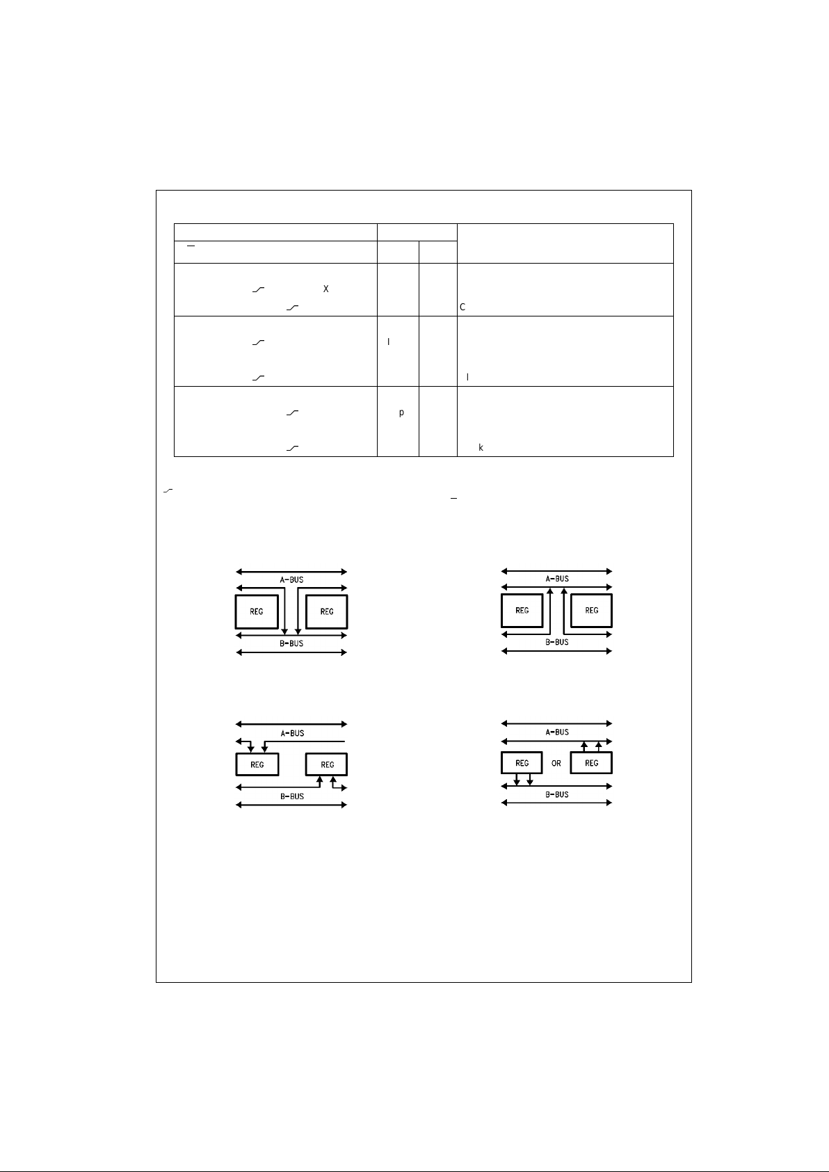
Function Table
H = HIGH Voltage Level
L = LOW Voltage Level
X = Irreleva nt
= LOW-to-HIGH Transition
Note 1: The data output functions may be enabled or disabled by various signals at the G
and DIR input s . D ata input func tions are always enabled; i.e., dat a
at the bus pins will be s to red on every LOW-to-HIG H tra ns it ion of the clock inputs.
Real Time Transfer
A-Bus to B-Bus
FIGURE 1.
Real Time Transfer
B-Bus to A-Bus
FIGURE 2.
Storage from
Bus to Register
FIGURE 3.
Transfer from
Register to Bus
FIGURE 4.
Inputs Data I/O (Note 1) Function
G
DIR CPAB CPBA SAB SBA A0–A7B0–B
7
H X H or L H or L X X Isolation
HX
X X X Input Input Clock An Data into A Register
HX X
X X Clock Bn Data into B Register
LHXXLX A
n
to Bn—Real Time (Transparent Mode)
LH
X L X Input Output Clock An Data into A Register
L H H or L X H X A Register to B
n
(Stored Mode)
LH
X H X Clock An Data into A Register and Output to B
n
LLXXXL Bn to An —Real Time (Transparent Mode)
LLX
X L Output Input Clock Bn Data into B Register
L L X H or L X H B Register to A
n
(Stored Mode)
LLX
X H Clock Bn Data into B Register and Output to A
n
Page 3

3 www.fairchildsemi.com
74AC648
Logic Diagram
Please note that this diagram is provided only for the understanding of logic operations and should not be used to estimate propagation delays.
Page 4

www.fairchildsemi.com 4
74AC648
Absolute Maximum Ratings(Note 2) Recommended Operating
Conditions
Note 2: Absolute maximum ratings are those values beyond which damage
to the device may occur. The databook specifications should be met, without exception, to ensure that the system design is reliable over its power
supply, temperature, and ou tput/inp ut loadi ng varia bles. Fairchild does no t
recommend operat ion of FACT circuits outside da t abook specifications.
DC Electrical Characteristics
Note 3: All outputs loaded; thresholds on input assoc iat ed with output under tes t.
Note 4: Maximum test duratio n 2. 0 ms, one output loaded at a time.
Note 5: I
IN
and ICC @ 3.0V are guaranteed to be less than or equa l to th e respective limit @ 5.5V VCC.
Supply Voltage (VCC) −0.5V to +7.0V
DC Input Diode Current (I
IK
)
V
I
= −0.5V −20 mA
V
I
= VCC + 0.5V +20 mA
DC Input Voltage (V
I
) −0.5V to VCC + 0.5V
DC Output Diode Current (I
OK
)
V
O
= −0.5V −20 mA
V
O
= V
CC
+ 0.5V +20 mA
DC Output Voltage (V
O
) −0.5V to VCC + 0.5V
DC Output Source
or Sink Current (I
O
) ± 50 mA
DC V
CC
or Ground Current
per Output Pin (I
CC
or I
GND
) ± 50 mA
Storage Temperature (T
STG
) −65°C to +150°C
Junction Temperature (T
J
)
PDIP 140
°C
Supply Voltage (V
CC
) 2.0V to 6.0V
Input Voltage (V
I
) 0V to V
CC
Output Voltage (VO) 0V to V
CC
Operating Temperature (TA) −40°C to +85°C
Minimum Input Edge Rate (
∆V/∆t) 125 mV/ns
V
IN
from 30% to 70% of V
CC
VCC @ 3.3V, 4.5V, 5.5V
Symbol Parameter
V
CC
TA = +25°C TA = −40°C to +85°C
Units Conditions
(V) Typ Guaranteed Limits
V
IH
Minimum HIGH Level 3.0 1.5 2.1 2.1 V
OUT
= 0.1V
Input Voltage 4.5 2.25 3.15 3.15 V or VCC − 0.1V
5.5 2.75 3.85 3.85
V
IL
Maximum LOW Level 3.0 1.5 0.9 0.9 V
OUT
= 0.1V
Input Voltage 4.5 2.25 1.35 1.35 V or VCC − 0.1V
5.5 2.75 1.65 1.65
V
OH
Minimum HIGH Level 3.0 2.99 2.9 2.9
Output Voltage 4.5 4.49 4.4 4.4 V I
OUT
= −50 µA
5.5 5.49 5.4 5.4
VIN = V
IL
or V
IH
3.0 2.56 2.46 IOH= −12 mA
4.5 3.86 3.76 V I
OH
= −24 mA
5.5 4.86 4.76 IOH= −24 mA (Note 3)
V
OL
Maximum LOW Level 3.0 0.002 0.1 0.1
Output Voltage 4.5 0.001 0.1 0.1 V I
OUT
= 50 µA
5.5 0.001 0.1 0.1
VIN = V
IL
or V
IH
3.0 0.36 0.44 IOL= 12 mA
4.5 0.36 0.44 V IOL = 24 mA
5.5 0.36 0.44 IOL = 24 mA (Note 3)
IIN Maximum Input
5.5 ±0.1 ±1.0 µAVI = VCC, GND
(Note 5) Leakage Current
I
OLD
Minimum Dynamic 5.5 75 mA V
OLD
= 1.65V Max
I
OHD
Output Current (Note 4) 5.5 −75 mA V
OHD
= 3.85V Min
I
CC
Maximum Quiescent
5.5 8.0 80.0 µA
VIN = V
CC
(Note 5) Supply Current or GND
I
OZT
Maximum I/O VI (OE) = VIL, V
IH
Leakage Current 5.5 ±0.6 ±6.0 µAVI = VCC, GND
VO = VCC, GND
Page 5

5 www.fairchildsemi.com
74AC648
AC Electrical Characteristics
Note 6: Voltage Range 3.3 is 3.3V ± 0.3V; Voltage Range 5.0 is 5.0V ± 0.5V
AC Operating Requirements
Note 7: Voltage Range 3.3 is 3.3V ± 0.3V; Voltage Range 5.0 is 5.0V ± 0.5V
Capacitance
V
CC
TA = +25°CT
A
= −40°C to +85°C
Symbol Parameter (V)
C
L
= 50 pF CL = 50 pF
Units
(Note 6) Min Typ Max Min Max
t
PLH
Propagation Delay 3.3 1.5 10.0 15.5 1.5 17.0
ns
Clock to Bus 5.0 1.5 7.0 11.0 1.5 12.0
t
PHL
Propagation Delay 3.3 1.5 8.5 13.5 1.5 14.5
ns
Clock to Bus 5.0 1.5 6.0 10.5 1.5 11.5
t
PLH
Propagation Delay 3.3 1.5 6.0 10.0 1.5 11.0
ns
Bus to Bus 5.0 1.5 4.0 7.0 1.0 7.5
t
PHL
Propagation Delay 3.3 1.5 5.5 9.0 1.5 10.0
ns
Bus to Bus 5.0 1.5 3.5 7.5 1.0 8.0
t
PLH
Propagation Delay 3.3 1.5 7.5 12.5 1.5 14.0
SBA or SAB to A
n
or B
n
5.0 1.5 5.5 9.0 1.5 10.0 ns
(with A
n
or Bn HIGH or LOW)
t
PHL
Propagation Delay 3.3 1.5 7.5 12.5 1.5 14.0
SBA or SAB to A
n
or B
n
5.0 1.5 5.5 9.5 1.5 10.5 ns
(with A
n
or Bn HIGH or LOW)
t
PZH
Enable Time 3.3 1.5 6.5 11.0 1.0 11.5
ns
G
to An or B
n
5.0 1.5 5.0 8.0 1.0 9.0
t
PZL
Enable Time 3.3 1.5 7.0 11.0 1.0 12.5
ns
G to An or B
n
5.0 1.5 5.0 8.0 1.0 9.0
t
PHZ
Disable Time 3.3 1.5 7.5 12.0 1.0 13.0
ns
G
to An or B
n
5.0 1.5 6.0 10.0 1.0 11.0
t
PLZ
Disable Time 3.3 1.5 7.0 11.5 1.0 12.5
ns
G
to An or B
n
5.0 1.5 5.5 9.0 1.0 10.0
t
PZH
Enable Time 3.3 1.5 6.0 12.5 1.0 14.0
ns
DIR to An or B
n
5.0 1.5 4.5 9.5 1.0 10.5
t
PZL
Enable Time 3.3 1.5 6.5 13.0 1.5 14.5
ns
DIR to A
n
or B
n
5.0 1.5 4.5 9.0 1.0 10.5
t
PHZ
Disable Time 3.3 1.5 7.0 11.5 1.0 13.5
ns
DIR to A
n
or B
n
5.0 1.5 5.5 9.0 1.0 10.0
t
PLZ
Disable Time 3.3 1.5 7.0 13.5 1.5 15.0
ns
DIR to An or B
n
5.0 1.5 5.0 9.5 1.0 10.0
V
CC
TA = +25°C T
A
= −40°C to +85°C
Symbol Parameter (V) CL = 50 pF CL = 50 pF Units
(Note 7) Typ Guaranteed Minimum
t
S
Setup Time, HIGH or LOW, 3.3 2.0 3.0 3 .5
ns
Bus to Clock 5.0 1.5 2.0 2.0
t
H
Hold Time, HIGH or LOW, 3.3 −1.5 0 0
ns
Bus to Clock 5.0 −0.5 1.0 1.0
t
W
Clock Pulse Width 3.3 2.0 3.5 4.0
ns
HIGH or LOW 5.0 2.0 3.0 3.0
Symbol Parameter Typ Units Conditions
C
IN
Input Capacitance 4.5 pF VCC = OPEN
C
PD
Power Dissipation Capacitance 65.0 pF VCC = 5.0V
C
I/O
Input/Output Capacitance 15.0 pF VCC = 5.0V
Page 6

www.fairchildsemi.com 6
74AC648
Physical Dimensions inches (millimeters) unless otherwise noted
24-Lead Small Outline Integrated Circuit (SOIC), JEDEC MS-013, 0.300 Wide
Package Number M24B
Page 7

7 www.fairchildsemi.com
74AC648 Octal Transceiver/Register with 3-STATE Outputs
Physical Dimensions inches (millimeters) unless otherwise noted (Continued)
24-Lead Plastic Dual-In-Line Package (PDIP), JEDEC MS-001, 0.300 Wide
Package Number N24C
Fairchild does not assume any responsibility for use of any circuitry described , no circuit patent licenses are implied and
Fairchild reserves the right at any time without notice to change said circuitry and specifications.
LIFE SUPPORT POLICY
FAIRCHILD’S PRODUCTS ARE NOT AUTHORIZED FOR USE AS CRITICAL COMPONENTS IN LIFE SUPPORT
DEVICES OR SYSTEMS WITHOUT THE EXPRESS WRITTEN APPROVAL OF THE PRESIDENT OF FAIRCHILD
SEMICONDUCTOR CORPORATION. As used herein:
1. Life support devices or systems are dev ic es or syste ms
which, (a) are intended for surgical implant into the
body, or (b) support or sustain life, and (c) whose failure
to perform when properly used in accordance with
instructions for use provide d in the labe l ing, can be re asonably expected to result in a significant injury to the
user.
2. A critical compo nent in any com ponen t of a life s upp ort
device or system whose failure to perform can be reasonably expected to cause the failure of the l ife support
device or system, or to affect its safety or effectiveness.
www.fairchildsemi.com
 Loading...