

Page 1
November 1988
Revised December 1998
74AC646 • 74ACT646 Octal Transceiver/Register with 3-STATE Outputs
© 1999 Fairchild Semiconductor Corporation DS010132.prf www.fairchildsemi.com
74AC646 • 74ACT646
Octal Transceiver/Register with 3-STATE Outputs
General Description
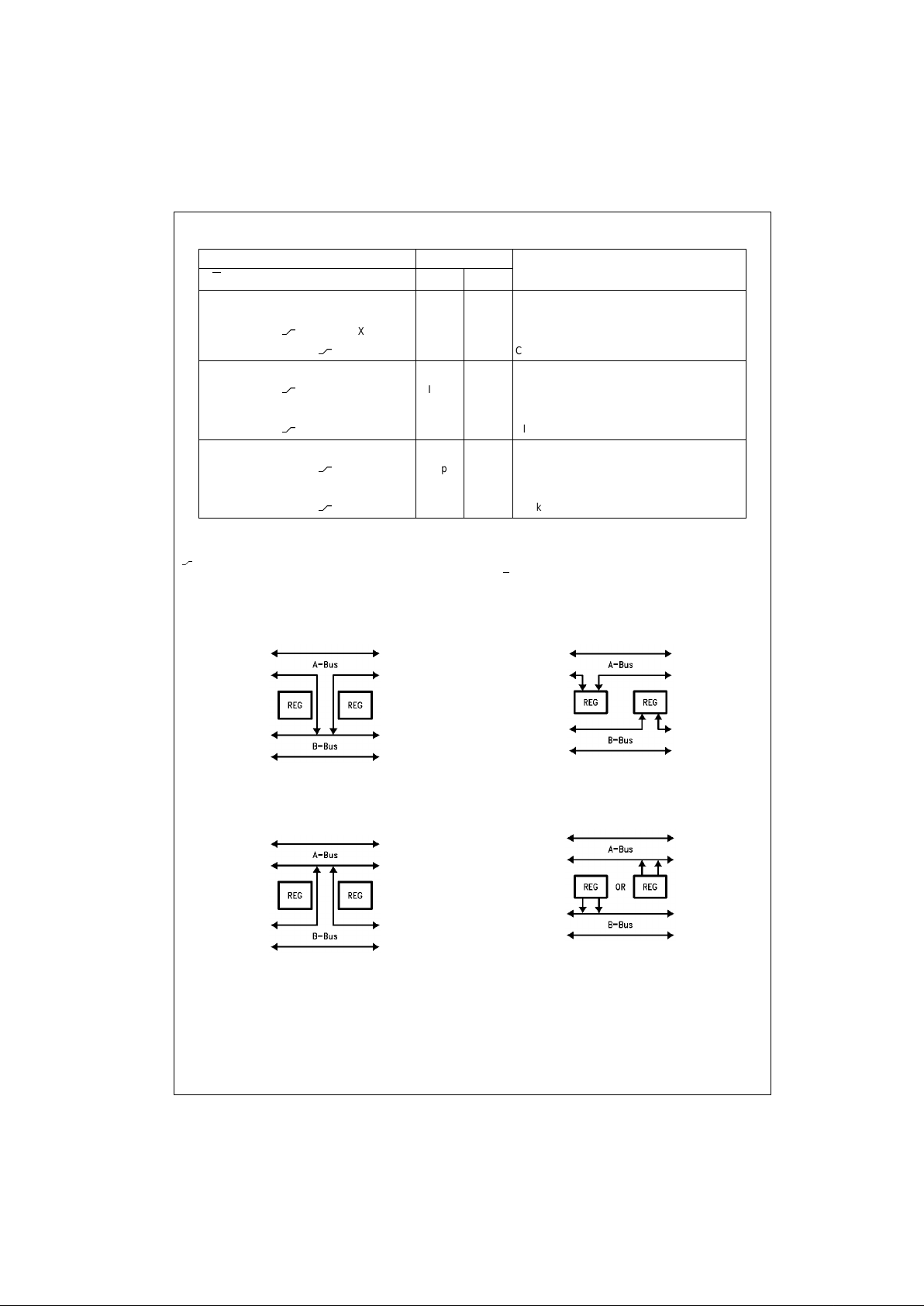
The AC/ACT646 consist of registe red bus transceiver circuits, with outputs, D-type flip-flops and control circuitry
providing multiplexed transmission of data directly from the
input bus or from the internal storage registers. Data on the
A or B bus will be loaded into the respective registers on
the LOW-to-HIGH transition of the appropriate clock pin
(CPAB or CPBA). The four fundamental data handling
functions available are illustrated in Figure 1, Figure 2, Figure 3, and Figure 4.
Features
■ Independent registers for A and B buses
■ Multiplexed real-time and stored data transfers
■ 3-STATE outputs
■ 300 mil dual-in-line package
■ Outputs source/sink 24 mA
■ ACT646 has TTL compatible inputs
Ordering Code:
Device also available in Tape and Reel. Specify by appendin g s uf f ix let t er “X” to the ordering co de.
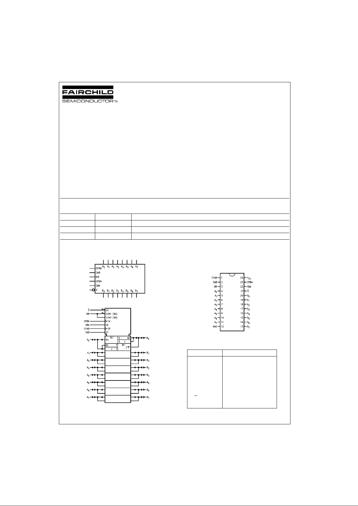
Logic Symbols
IEEE/IEC
Connection Diagram
Pin Assignment
for DIP and SOIC
Pin Descriptions
FACT is a tra demark of Fairchild Semico nductor Corporation.
Order Number Package Number Package Description
74AC646SC M24B 24-Lead Small Outline Integrated Circuit (SOIC), JEDEC MS-013, 0.300” Wide Body
74AC646SPC N24C 24-Lead Plastic Dual-In-Line Package (PDIP), JEDEC MS-100, 0.300” Wide
74ACT646SPC N24C 24-Lead Plastic Dual-In-Line Package (PDIP), JEDEC MS-100, 0.300” Wide
Pin Names Description
A
0–A7
Data Register A Inputs
Data Register A Outputs
B
0–B7
Data Register B Inputs
Data Register B Outputs
CPAB, CPBA Clock Pulse Inputs
SAB, SBA Transmit/Receive Inputs
G
Output Enable Input
DIR Direction Control Input
Page 2
www.fairchildsemi.com 2
74AC646 • 74ACT646
Function Table
H = HIGH Voltage Level
L = LOW V oltage Leve l
X = Immaterial
= LOW-to-HIGH Transition
Note 1: The data output fu nc t ions may be enabled or disabled by various signals at the G
and DIR inputs. Data input functions are always enabled; i.e., data
at the bus pins will be stored on every LOW-to-HIGH transition of t he appropriate clock inputs.
Real Time Transfer
A-Bus to B-Bus
FIGURE 1.
Real Time Transfer
B-Bus to A-Bus
FIGURE 2.
Storage from
Bus to Register
FIGURE 3.
Transfer from
Register to Bus
FIGURE 4.
Inputs Data I/O (Note 1) Function
G
DIR CPAB CPBA SAB SBA A0–A7B0–B
7
H X H or L H or LXX Isolation
HX
X X X Input Input Clock An Data into A Register
HXX
X X Clock Bn Data into B Register
LHXXLX A
n
to Bn—Real Time (Transparent Mode)
LH
X L X Input Output Clock An Data into A Register
L H H or L X H X A Register to B
n
(Stored Mode)
LH
X H X Clock An Data into A Register and Output to B
n
LLXXXL Bn to An —Real Time (Transparent Mode)
LLX
X L Output Input Clock Bn Data into B Register
L L X H or L X H B Register to A
n
(Stored Mode)
LLX
X H Clock Bn Data into B Register and Output to A
n
Page 3
3 www.fairchildsemi.com
74AC646 • 74ACT646
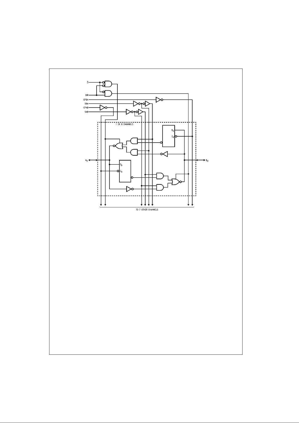
Logic Diagram
Please note that this d iagram is provided only for the understanding of logic operations and should no t b e us ed to estimate propagation delays.
Page 4

www.fairchildsemi.com 4
74AC646 • 74ACT646
Absolute Maximum Ratings(Note 2) Recommended Operating
Conditions
Note 2: Absolute maximum ratings are thos e value s beyond wh ic h dam age
to the device may occur. The databook specif ications should b e met, wit hout exception, to ensure th at the system design is reliable over its power
supply, temperature, and output/inp ut loading variables. Fairchild does no t
recommend operat ion of FACT circuits outside databook specifications.
DC Electrical Characteristics for AC
Note 3: All outputs loaded; thresholds on input associated wit h output under test.
Note 4: Maximum test duration 2.0 ms, one output loaded at a time.
Note 5: I
IN
and ICC @ 3.0V are guaranteed to be less than or equal t o t he respective limit @ 5.5V VCC.
Supply Voltage (VCC) −0.5V to +7.0V
DC Input Diode Current (I
IK
)
V
I
= −0.5V −20 mA
V
I
= VCC + 0.5V +20 mA
DC Input Voltage (V
I
) −0.5V to VCC + 0.5V
DC Output Diode Current (I
OK
)
V
O
= −0.5V −20 mA
V
O
= VCC + 0.5V +20 mA
DC Output Voltage (V
O
) −0.5V to VCC + 0.5V
DC Output Source
or Sink Current (I
O
) ±50 mA
DC V
CC
or Ground Current
per Output Pin (I
CC
or I
GND
) ±50 mA
Storage Temperature (T
STG
) −65°C to +150°C
Junction Temperature (T
J
)
PDIP 140°C
Supply Voltage (V
CC
)
AC 2.0V to 6.0V
ACT 4.5V to 5.5V
Input Voltage (V
I
) 0V to V
CC
Output Voltage (VO) 0V to V
CC
Operating Temperature (TA) −40°C to +85°C
Minimum Input Edge Rate (∆V/∆t)
AC Devices
V
IN
from 30% to 70% of V
CC
VCC @ 3.3V, 4.5V, 5.5V 125 mV/ns
Minimum Input Edge Rate (∆V/∆t)
ACT Devices
V
IN
from 0.8V to 2.0V
V
CC
@ 4.5V, 5.5V 125 mV/ns
Symbol Parameter
V
CC
TA = +25°C TA = −40°C to +85°C
Units Conditions
(V) Typ Guaranteed Limits
V
IH
Minimum HIGH Level 3.0 1.5 2.1 2.1 V
OUT
= 0.1V
Input Voltage 4.5 2.25 3.15 3.15 V or VCC − 0.1V
5.5 2.75 3.85 3.85
V
IL
Maximum LOW Level 3.0 1.5 0.9 0.9 V
OUT
= 0.1V
Input Voltage 4.5 2.25 1.35 1.35 V or VCC − 0.1V
5.5 2.75 1.65 1.65
V
OH
Minimum HIGH Level 3.0 2.99 2.9 2.9 I
OUT
= −50 µA
Output Voltage 4.5 4.49 4.4 4.4 V
5.5 5.49 5.4 5.4
VIN = VIL or V
IH
3.0 2.56 2.46 IOH = −12 mA
4.5 3.86 3.76 V IOH = −24 mA
5.5 4.86 4.76 IOH = −24 mA (Note 3)
V
OL
Maximum LOW Level 3.0 0.002 0.1 0.1 I
OUT
= 50 µA
Output Voltage 4.5 0.001 0.1 0.1 V
5.5 0.001 0.1 0.1
VIN = VIL or V
IH
3.0 0.36 0.44 IOH = 12 mA
4.5 0.36 0.44 V IOL = 24 mA
5.5 0.36 0.44 IOH = 24 mA (Note 3)
IIN (Note 5) Maximum Input Leakage Current 5.5 ± 0.1 ± 1.0 µAVI = VCC, GND
I
OLD
Minimum Dynamic 5.5 75 mA V
OLD
= 1.65V Max
I
OHD
Output Current (Note 4) 5.5 −75 mA V
OHD
= 3.85V Min
I
CC
(Note 5) Maximum Quiescent Supply Current 5.5 8.0 80.0 µAVIN = VCC or GND
I
OZT
Maximum I/O VI (OE) = VIL, V
IH
Leakage Current 5.5 ±0.6 ±6.0 µAVI = VCC, GND
VO = VCC, GND
Page 5

5 www.fairchildsemi.com
74AC646 • 74ACT646
DC Electrical Characteristics for ACT
Note 6: All outputs loaded; thresholds on input associated with ou t put under test.
Note 7: Maximum test duration 2.0 ms, one output loaded at a time.
AC Electrical Characteristics for AC
Symbol Parameter V
CC
TA = +25°C TA = −40°C to +85°C Units Conditions
(V) Typ Guaranteed Limits
V
IH
Minimum HIGH Level 4.5 1.5 2.0 2.0 V V
OUT
= 0.1V
Input Voltage 5.5 1.5 2.0 2.0 or VCC − 0.1V
V
IL
Maximum LOW Level 4.5 1.5 0.8 0.8 V V
OUT
= 0.1V
Input Voltage 5.5 1.5 0.8 0.8 or VCC − 0.1V
V
OH
Minimum HIGH Level 4.5 4.49 4.4 4.4 V I
OUT
= −50 µA
Output Voltage 5.5 5.49 5.4 5.4
VIN = VIL or V
IH
4.5 3.86 3.76 V IOH= −24 mA
5.5 4.86 4.76 IOH= −24 mA (Note 6)
V
OL
Maximum LOW Level 4.5 0.001 0.1 0.1 V I
OUT
= 50 µA
Output Voltage 5.5 0.001 0.1 0.1
VIN = VIL or V
IH
4.5 0.36 0.44 V IOL= 24 mA
5.5 0.36 0.44 IOL = 24 mA (Note 6)
Maximum Input
Leakage Current
5.5 ± 0.1 ± 1.0 µAVI = VCC, GND
Maximum
ICC/Input
5.5 0.6 1.5 mA
VI = VCC − 2.1V
I
OLD
Minimum Dynamic 5.5 75 mA V
OLD
= 1.65V Max
I
OHD
Output Current (Note 7) 5.5 −75 mA V
OHD
= 3.85V Min
I
CC
Maximum Quiescent 5.5 8.0 80.0 µA VIN = V
CC
Supply Current or GND
I
OZT
Maximum I/O VI (OE) = VIL, V
IH
Leakage Current 5.5 ±0.6 ±6.0 µAVI = VCC, GND
VO = VCC, GND
V
CC
TA = +25°CT
A
= −40°C to +85°C
Symbol Parameter (V)
CL = 50 pF CL = 50 pF
Units
(Note 8) Min Typ Max Min Max
t
PLH
Propagation Delay 3.3 4.0 10.5 16.5 3.0 18.5 ns
Clock to Bus 5.0 2.5 7.5 12.0 2.0 13.0
t
PHL
Propagation Delay 3.3 3.0 9.5 14.5 2.5 16.0 ns
Clock to Bus 5.0 2.0 6.5 10.5 1.5 11.5
t
PLH
Propagation Delay 3.3 2.5 7.5 12.0 2.0 13.5 ns
Bus to Bus 5.0 1.5 5.0 8.0 1.0 9.0
t
PHL
Propagation Delay 3.3 1.5 7.5 12.5 1.5 13.5 ns
Bus to Bus 5.0 1.5 5.0 9.0 1.0 9.5
t
PLH
Propagation Delay 3.3 2.0 8.5 13.5 1.5 15.5
SBA or SAB to An or B
n
5.0 1.5 6.0 10.0 1.5 11.0 ns
(w/ An or Bn HIGH or LOW)
t
PHL
Propagation Delay 3.3 1.5 8.5 13.5 1.5 15.0
SBA or SAB to An or B
n
5.0 1.5 6.0 10.0 1.5 11.0 ns
(w/ An or Bn HIGH or LOW)
t
PZH
Enable Time 3.3 2.5 7.0 11.5 2.0 12.5 ns
G to An or B
n
5.0 1.5 5.0 8.5 1.5 9.0
Page 6

www.fairchildsemi.com 6
74AC646 • 74ACT646
AC Electrical Charac teristics for AC (Continued)
Note 8: Voltage Range 3.3 is 3.3V ±0.3V
Voltage Range 5.0 is 5.0V ±0.5V
AC Operating Requirements for AC
Note 9: Voltage Range 3.3 is 3.3V ±0.3V
Voltage Range 5.0 is 5.0V ±0.5V
V
CC
TA = +25°CT
A
= −40°C to +85°C
Symbol Parameter (V)
CL = 50 pF CL = 50 pF
Units
(Note 8) Min Typ Max Min Max
t
PZL
Enable Time 3.3 2.5 7.5 12.5 2.0 14.0 ns
G to An or B
n
5.0 1.5 5.5 9.0 1.5 10.0
t
PHZ
Disable Time 3.3 3.0 8.0 12.5 2.5 13.5 ns
G to An or B
n
5.0 2.0 6.5 10.0 2.0 11.0
t
PLZ
Disable Time 3.3 2.0 7.5 12.0 2.0 13.5 ns
G to An or B
n
5.0 1.5 6.0 9.5 1.5 10.5
t
PZH
Enable Time 3.3 2.0 6.5 11.0 1.5 12.0 ns
DIR to An or B
n
5.0 1.5 5.0 7.5 1.0 8.5
t
PZL
Enable Time 3.3 2.5 7.0 11.5 2.0 13.0 ns
DIR to An or B
n
5.0 1.5 5.0 8.0 1.0 9.0
t
PHZ
Disable Time 3.3 2.5 7.5 11.5 1.5 12.5 ns
DIR to An or B
n
5.0 1.5 5.5 9.5 1.5 10.0
t
PLZ
Disable Time 3.3 1.5 7.5 12.0 1.5 13.5 ns
DIR to An or B
n
5.0 1.5 5.5 9.5 1.5 10.5
V
CC
TA = +25°CT
A
= −40°C to +85°C
Symbol Parameter (V)
CL = 50 pF CL = 50 pF
Units
(Note 9) Typ Guaranteed Minimum
t
S
Setup Time, HIGH or LOW 3.3 2.0 5.0 5.5 ns
Bus to Clock 5.0 1.5 4.0 4.5
t
H
Hold Time, HIGH or LOW 3.3 −1.5 0 0 ns
Bus to Clock 5.0 −0.5 0.5 1.0
t
W
Clock Pulse Width 3.3 2.0 3.5 4.5 ns
HIGH or LOW 5.0 2.0 3.5 3.5
Page 7

7 www.fairchildsemi.com
74AC646 • 74ACT646
AC Electrical Characteristics for AC T
Note 10: Voltage Range 5.0 is 5.0V ±0.5V
V
CC
TA = +25°CT
A
= −40°C to +85°C
Symbol Parameter (V)
CL = 50 pF CL = 50 pF
Units
(Note 10) Min Typ Max Min Max
t
PLH
Propagation Delay 5.0 3.5 12.0 14.5 3.0 16.0 ns
Clock to Bus
t
PHL
Propagation Delay 5.0 4.0 12.0 14.5 3.5 16.0 ns
Clock to Bus
t
PLH
Propagation Delay 5.0 3.0 8.5 10.5 2.5 11.5 ns
Bus to Bus
t
PHL
Propagation Delay 5.0 2.5 8.5 10.5 2.0 11.5 ns
Bus to Bus
t
PLH
Propagation Delay
SBA or SAB to An to B
n
5.0 3.0 9.5 11.5 2.5 12.5 ns
(w/An or B
n
HIGH or LOW)
t
PHL
Propagation Delay
SBA or SAB to An to B
n
5.0 3.0 9.5 11.5 2.5 12.5 ns
(w/An or B
n
HIGH or LOW)
t
PZH
Enable Time 5.0 2.0 9.0 11.0 1.5 12.0 ns
G to An or B
n
t
PZL
Enable Time 5.0 3.5 9.0 11.0 3.0 12.0 ns
G to An or B
n
t
PHZ
Disable Time 5.0 5.0 10.5 13.0 4.5 14.5 ns
G to An or B
n
t
PLZ
Disable Time 5.0 3.5 10.0 12.5 3.0 14.0 ns
G to An or B
n
t
PZH
Enable Time 5.0 2.0 6.5 10.5 1.5 11.5 ns
DIR to An or B
n
t
PZL
Enable Time 5.0 3.5 6.5 10.5 3.0 11.5 ns
DIR to An or B
n
t
PHZ
Disable Time 5.0 5.0 8.5 12.5 4.5 13.5 ns
DIR to An or B
n
t
PLZ
Disable Time 5.0 3.5 8.5 12.5 3.0 13.5 ns
DIR to An or B
n
Page 8

www.fairchildsemi.com 8
74AC646 • 74ACT646
AC Operating Requirements for ACT
Note 11: Voltage Range 5.0 is 5.0V ±0.5V
Capacitance
V
CC
TA = +25°C T
A
= −40°C to +85°C
Symbol Parameter (V)
CL = 50 pF CL = 50 pF
Units
(Note 11) Typ Guaranteed Minimum
t
S
Setup Time, HIGH or LOW 5.0 2.5 7.0 8.0 ns
BUS to Clock
t
H
Hold Time, HIGH or LOW 5.0 0 2.5 2.5 ns
Bus to Clock
t
W
Clock Pulse Width 5.0 4.5 7.0 8.0 ns
HIGH or LOW
Symbol Parameter Typ Units Conditions
C
IN
Input Capacitance 4.5 pF VCC = OPEN
C
I/O
Input/Output Capacitance 15.0 pF VCC = 5.0V
C
PD
Power Dissipation Capacitance 60.0 pF VCC = 5.0V
Page 9

9 www.fairchildsemi.com
74AC646 • 74ACT646
Physical Dimensions inches (millimeters) unless otherwise noted
24-Lead Small Outline Integrated Circuit (SOIC), JEDEC MS-013, 0.300” Wide Body
Package Number M24B
Page 10

Fairchild does not assume any responsibility for use of any circuitry described, no circuit patent licenses are implied and Fairchild reser ves the right at any time without notice to change said circuitry and specifications.
74AC646 • 74ACT646 Octal Transceiver/Register with 3-STATE Outputs
LIFE SUPPORT POLICY
FAIRCHILD’S PRODUCTS ARE NOT AUTHORIZED FOR USE AS CRITICAL COMPONENTS IN LIFE SUPPORT
DEVICES OR SYSTEMS WITHOUT THE EXPRESS WRITTEN APPROVAL OF THE PRESIDENT OF FAIRCHILD
SEMICONDUCTOR CORPORATION. As used herein:
1. Life support devices or system s ar e devices or syste ms
which, (a) are intended for surgical implant into the
body, or (b) support or sustain life, and (c) whose failure
to perform when properly used in accordance with
instructions for use provided in the labeling, can be reasonably expected to result in a significant injury to the
user.
2. A critical component in any c omponent of a life suppor t
device or system whose failure to perform can be reasonably expected to cause the failure of the life suppor t
device or system, or to affect its safety or effectiveness.
www.fairchildsemi.com
Physical Dimensions inches (millimeters) unless otherwise noted (Continued)
24-Lead Plastic Dual-In-Line Package (PDIP), JEDEC MS-100, 0.300” Wide
Package Number N24C
 Loading...