

Page 1
74AC573
OCTAL D-TYPE LATCH
WITH 3 STATE OUTPUT NON INVERTING
■ HIGH SPEED: t
■ LOWPOWER DISSIPATION:
=8µA (MAX.) at TA=25oC
I
CC
■ HIGH NOISE IMMUNITY:
V
NIH=VNIL
■ 50Ω TRANSMISSIONLINE DRIVING
= 4.5 ns(TYP.) at VCC=5V
PD
=28%VCC(MIN.)
CAPABILITY
■ SYMMETRICAL OUTPUT IMPEDANCE:
|I
|=IOL=24 mA (MIN)
OH
■ BALANCEDPROPAGATIONDELAY S:
t
≅ t
PLH
PHL
■ OPERATINGVOLTAGERAN GE:
V
(OPR) = 2V to 6V
CC
■ PIN AND FUNCTION COMPATIBLE WITH
74SERIES573
■ IMPROVED LATCH-UP IMMUNITY
DESCRIPTION
The AC573 is an advanced high-speed CMOS
OCTAL D-TYPE LATCH with 3 STATE OUTPUT
NON INVERTING fabricated with sub-micron
silicon gate and double-layermetal wiringC
2
MOS
technology. It is ideal for low power applications
mantaining high speed operation similar to
equivalentBipolarSchottkyTTL.
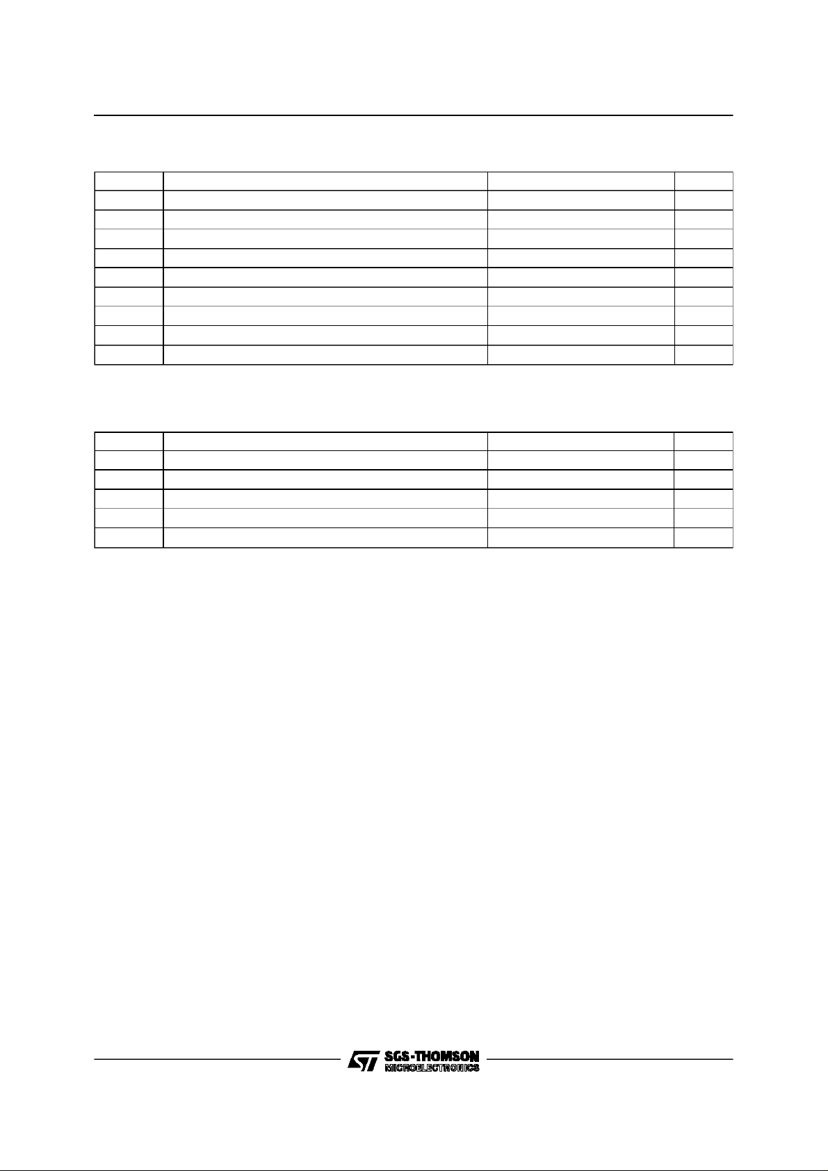
These 8 bit D-Type latches are controlled by a
B
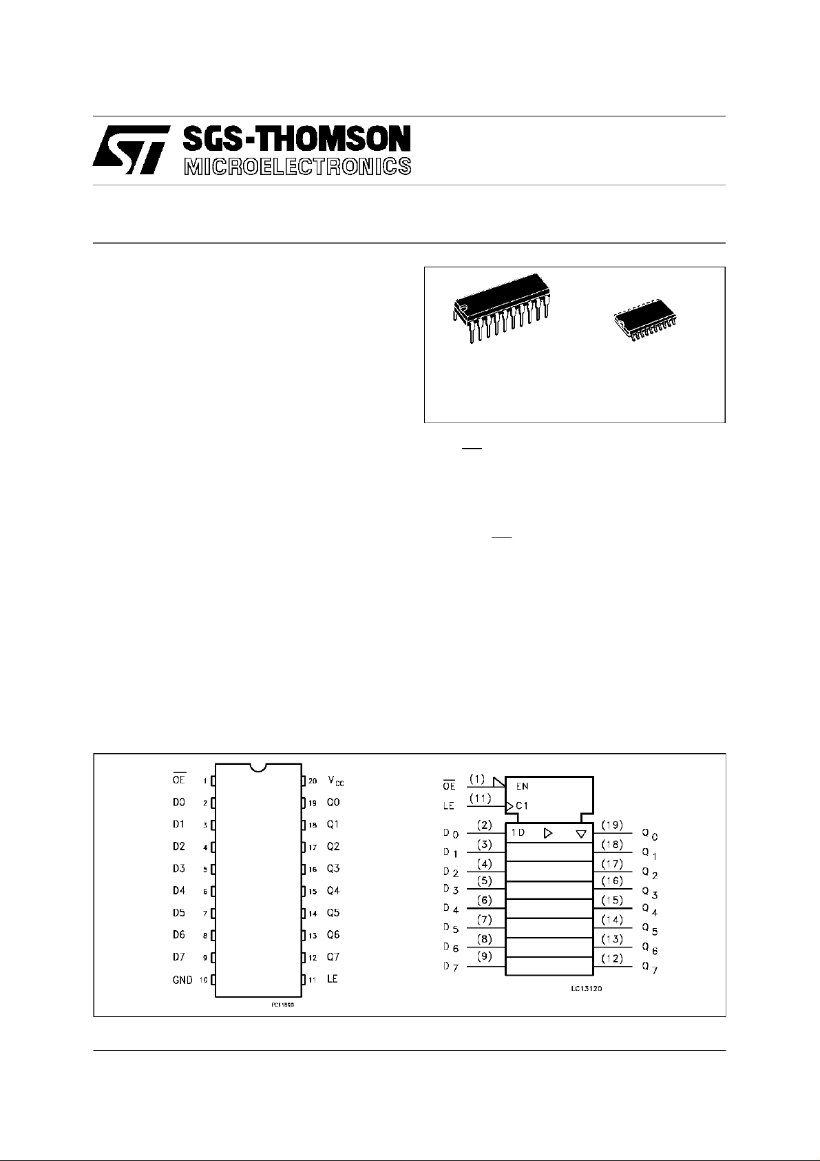
(Plastic Package)
(Micro Package)
M
ORDERCODES:
74AC573B 74AC573M
latch enable input (LE) and an output enable
input (OE).
While the LE input is held at a high level, the Q
outputswill follow the data input precisely.
When the LE is taken low, the Q outputs will be
latchedpreciselyat thelogic level of D inputdata.
While the (OE) input is low, the 8 outputs will be
in a normal logic state (high or low logic level)
and while high level the outputs will be in a high
impedancestate.
All inputs and outputs are equipped with
protectioncircuits against static discharge, giving
them 2KV ESD immunity and transient excess
voltage.
PINCONNECTION AND IEC LOGICSYMBOLS
April 1997
1/10
Page 2
74AC573
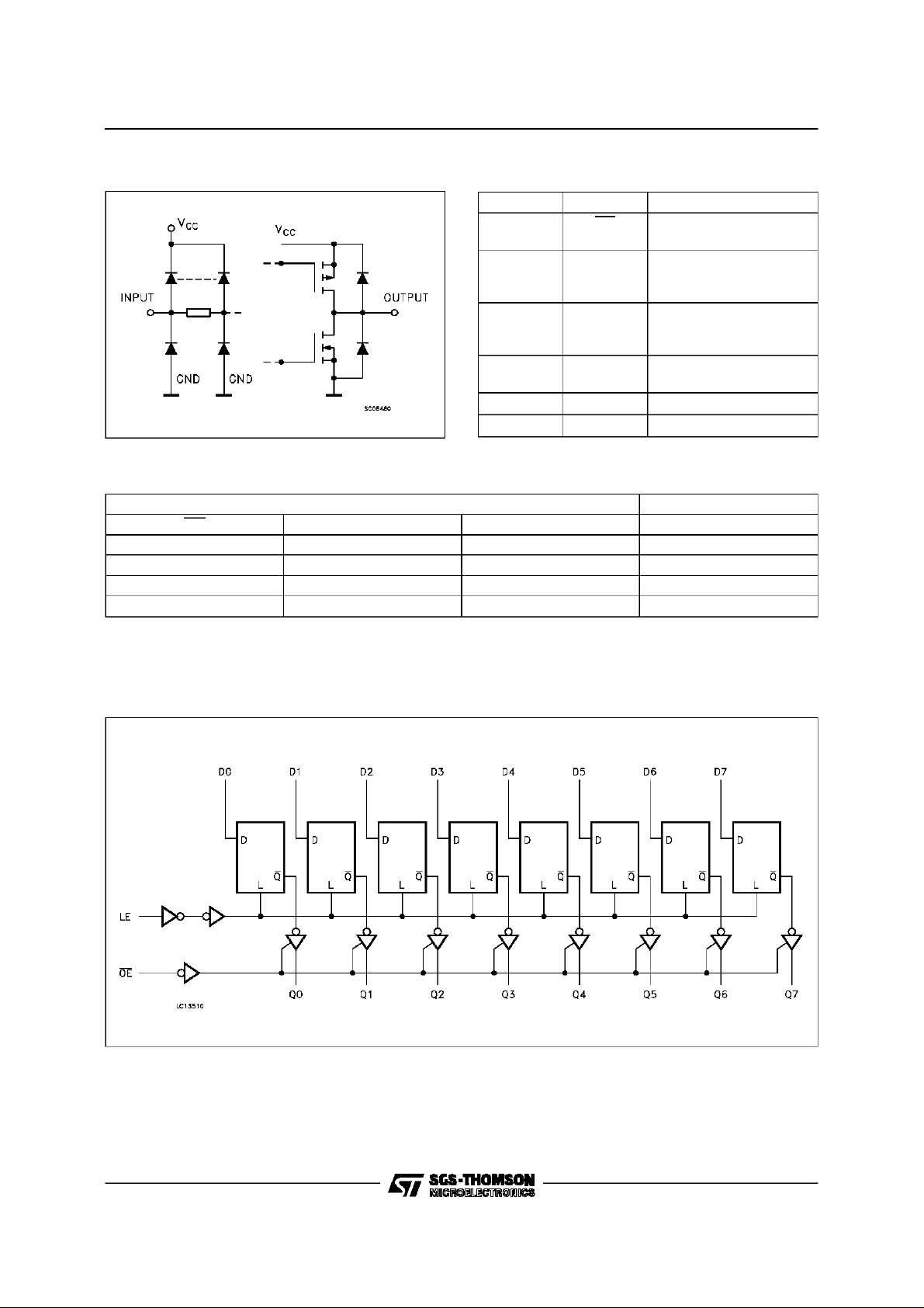
INPUTAND OUTPUTEQUIVALENTCIRCUIT PIN DESCRIPTION
PI N No SYM B O L NAME AND F UNC T I ON
1 OE 3 State Output Enable
2, 3, 4,
5, 6, 7,
8, 9
12, 13, 14,
15, 16, 17,
18, 19
11 LE Latch Enable
10 GND Ground (0V)
20 V
TRUTH TABLE
INPUTS OUTPUTS
OE LE D Q
HXXZ
L L X NO CHANGE *
LHLL
LHHH
X:Don’tcare
Z: High impedance
* Q output are latched at the timewhen the LEinputs taken low logic level.
D0 to D7 Data Inputs
Q0 to Q7 3 State Latch Outputs
CC
Input (Active LOW)
Input
Positive Supply Voltage
LOGICDIAGRAM
2/10
Page 3
74AC573
ABSOLUTE MAXIMUM RATINGS
Symb o l Parameter Val u e Uni t
V
V
V
I
I
OK
I
orI
I
CC
T
T
Absolute Maximum Ratings are those values beyond which damage to the device may occur. Functional operation under these condition is not implied.
RECOMMENDED OPERATINGCONDITIONS
Symb o l Parameter Value Un i t
V
V
V
T
dt/dv Input Rise and Fall Time V
1) VINfrom30%to70%of V
Supply Voltage -0.5 to +7 V
CC
DC Input Voltage -0.5 to VCC+ 0.5 V
I
DC Output Voltage -0.5 to VCC+ 0.5 V
O
DC Input Diode Current ± 20 mA
IK
DC Output Diode Current ± 20 mA
DC Output Current ± 50 mA
O
DC VCCor Ground Current ± 400 mA
GND
Storage Temperature -65 to +150
stg
Lead Temperature (10 sec) 300
L
Supply Voltage 2 to 6 V
CC
Input Voltage 0 to V
I
Output Voltage 0 to V
O
Operating Temperature: -40 to +85
op
= 3.0, 4.5 or 5.5 V(note 1) 8 ns/V
CC
CC
CC
CC
o
C
o
C
V
V
o
C
3/10
Page 4

74AC573
DC SPECIFICATIONS
Symbol Parameter Test Condition s Value Unit
V
CC
(V)
High Level Input Voltage 3.0 VO= 0.1 V or
V
IH
4.5 3.15 2.25 3.15
V
CC
- 0.1 V
T
=25oC-40to85
A
Min. Typ. Max. Min . Max.
2.1 1.5 2.1
o
C
5.5 3.85 2.75 3.85
Low Level Input Voltage 3.0 VO= 0.1 V or
V
IL
4.5 2.25 1.35 1.35
V
CC
- 0.1 V
1.5 0.9 0.9
5.5 2.75 1.65 1.65
High Level Output
V
OH
Voltage
Low Level Output
V
OL
Voltage
Input Leakage Current
I
I
3-State Output Off-state
I
OZ
Current
Quiescent Supply
I
CC
3.0
4.5 I
5.5 I
V
V
3.0 I
4.5 I
5.5 I
3.0
4.5 I
5.5 I
V
V
3.0 I
4.5 I
5.5 I
5.5
5.5 VI=VCCor GND
V
IO=-50 µA 2.9 2.99 2.9
(*)
I
IH
V
IL
=-50 µA 4.4 4.49 4.4
O
=
=-50 µA 5.4 5.49 5.4
or
O
=-12 mA 2.56 2.46
O
=-24 mA 3.86 3.76
O
=-24 mA 4.86 4.76
O
IO=50 µA 0.002 0.1 0.1
(*)
I
IH
V
IL
=50 µA 0.001 0.1 0.1
O
=
=50 µA 0.001 0.1 0.1
or
O
=12 mA 0.36 0.44
O
=24 mA 0.36 0.44
O
=24 mA 0.36 0.44
O
VI=VCCor GND ±0.1 ±1 µA
±0.5 ±5 µA
V
I(OE)=VIH
or GND
O=VCC
5.5 VI=VCCor GND 8 80 µA
Current
Dynamic Output Current
I
OLD
OHD
(note 1, 2)
I
1) Maximum test duration 2ms, one output loaded at time
2) Incident wave switching is guaranteed on transmission lines with impedances as low as 50 Ω.
(*)All outputs loaded.
5.5 V
= 1.65 V max 75 mA
OLD
V
= 3.85 V min -75 mA
OHD
V
V
V
V
4/10
Page 5

AC ELECTRICAL CHARACTERISTICS (CL= 50 pF, RL=500 Ω, Inputtr=tf=3ns)
74AC573
Symbol Parameter Test Conditi on Value Unit
o
C
ns
ns
ns
ns
ns
ns
ns
t
Propagation Delay Time
PLH
t
LE to Q
PHL
Propagation Delay Time
t
PLH
t
DtoQ
PHL
Output EnableTime 3.3
t
PZL
t
PZH
Output Disable Time 3.3
t
PLZ
t
PHZ
t
Clock Pulse Width HIGH
w
or LOW
Setup Time Q to CK
t
s
HIGH or LOW
Hold Time Q to CK
t
h
HIGH or LOW
(*) Voltagerangeis 3.3V± 0.3V
(**) Voltagerangeis5V± 0.5V
V
3.3
5.0
3.3
5.0
5.0
5.0
3.3
5.0
3.3
5.0
3.3
5.0
(V)
CC
(**)
(**)
(**)
(**)
(**)
(**)
(**)
T
=25oC-40to85
A
Min. Typ. Max. Min . Max.
(*)
610 12
4.5 8 9
(*)
5.5 10 12
4.5 8 9
(*)
6.5 11 13
59 10
(*)
712 14
610 11
(*)
1.5 4 4.5
1.5 3.5 4
(*)
0.5 3 3.5
0 2.5 3
(*)
-0.5 3 3.5
0 2.5 3
CAPACITIVE CHARACTERISTICS
Symbol Parameter Test Condition s Value Unit
T
V
CC
(V)
C
Output Capacitance
OUT
Input Capacitance
C
IN
Power Dissipation
C
PD
5.0
5.0
5.0 20 pF
=25oC-40to85
A
Min. Typ. Max. Min . Max.
8
4
Capacitance (note 1)
1) CPDis defined as the value of the IC’s internal equivalent capacitance which is calculated from the operating current consumption without load. (Refer to
Test Circuit). Average operating current can be obtained by the following equation. I
(opr) = CPD• VCC•fIN+ICC/n (percircuit)
CC
o
C
pF
pF
5/10
Page 6

74AC573
TEST CIRCUIT
TEST SWITCH
t
PLH,tPHL
t
PZL,tPLZ
t
PZH,tPHZ
CL= 50 pF or equivalent (includes jig and probe capacitance)
= 500Ω or equivalent
R
L=R1
R
of pulse generator (typically 50Ω)
T=ZOUT
Open
2V
CC
Open
WAVEFORM 1: LE TO Qn PROPAGATION DELAYS, LE MINIMUM PULSE WIDTH,
Dn TOLE SETUPAND HOLD TIMES(f=1MHz;50% dutycycle)
6/10
Page 7

WAVEFORM 2: OUTPUTENABLE AND DISABLE TIMES (f=1MHz; 50% duty cycle)
74AC573
WAVEFORM 3: PROPAGATION DELAY TIME (f=1MHz; 50% duty cycle)
7/10
Page 8

74AC573
Plastic DIP20 (0.25) MECHANICAL DATA
DIM.
MIN. TYP. MAX. MIN. TYP. MAX.
a1 0.254 0.010
B 1.39 1.65 0.055 0.065
b 0.45 0.018
b1 0.25 0.010
D 25.4 1.000
E 8.5 0.335
e 2.54 0.100
e3 22.86 0.900
F 7.1 0.280
I 3.93 0.155
L 3.3 0.130
Z 1.34 0.053
mm inch
8/10
P001J
Page 9

SO20 MECHANICAL DATA
74AC573
DIM.
MIN. TYP. MAX. MIN. TYP. MAX.
A 2.65 0.104
a1 0.10 0.20 0.004 0.007
a2 2.45 0.096
b 0.35 0.49 0.013 0.019
b1 0.23 0.32 0.009 0.012
C 0.50 0.020
c1 45° (typ.)
D 12.60 13.00 0.496 0.512
E 10.00 10.65 0.393 0.419
e 1.27 0.050
e3 11.43 0.450
F 7.40 7.60 0.291 0.299
L 0.50 1.27 0.19 0.050
M 0.75 0.029
S8°(max.)
mm inch
P013L
9/10
Page 10

74AC573
Information furnished is believedto be accurateand reliable. However, SGS-THOMSONMicroelectronicsassumes no responsability for the
consequencesof use ofsuch information nor for anyinfringement of patentsor other rights ofthird parties whichmay results from its use. No
licenseisgrantedby implicationor otherwise underany patentor patent rights of SGS-THOMSONMicroelectronics. Specificationsmentioned
in this publicationare subjectto change without notice.This publication supersedes and replacesall information previouslysupplied.
SGS-THOMSONMicroelectronics productsare notauthorized for useascriticalcomponents inlifesupportdevices or systems withoutexpress
writtenapproval of SGS-THOMSONMicroelectonics.
1997 SGS-THOMSONMicroelectronics- Printedin Italy- AllRights Reserved
Australia- Brazil - Canada- China- France- Germany- HongKong - Italy- Japan- Korea- Malaysia- Malta- Morocco- TheNetherlands -
Singapore- Spain- Sweden- Switzerland- Taiwan - Thailand - United Kingdom- U.S.A
SGS-THOMSONMicroelectronics GROUPOF COMPANIES
.
10/10
 Loading...