

Page 1
74AC373
OCTAL D-TYPE LATCH
WITH 3 STATE OUTPUT NON INVERTING
■ HIGH SPEED: t
■ LOWPOWERDISSIPATION:
=8µA (MAX.)at TA=25oC
I
CC
■ HIGH NOISE IMMUNITY:
V
NIH=VNIL
■ 50Ω TRANSMISSION LINE DRIVING
=5 ns (TYP.)atVCC=5V
PD
=28%VCC(MIN.)
CAPABILITY
■ SYMMETRICAL OUTPUT IMPEDANCE:
|I
|=IOL=24mA(MIN)
OH
■ BALANCE DPROPAGATIONDELAYS:
t
≅ t
PLH
PHL
■ OPERATINGVOLTAGERAN GE:
V
(OPR) = 2V to 6V
CC
■ PIN AND FUNCTION COMPATIBLE WITH
74SERIES373
■ IMPROVED LATCH-UP IMMUNITY
DESCRIPTION
The AC373 is an advanced high-speed CMOS
OCTAL D-TYPE LATCH with 3 STATE OUTPUT
NON INVERTING fabricated with sub-micron
silicon gate and double-layermetal wiring C
2
MOS
technology. It is ideal for low power applications
mantaining high speed operation similar to
equivalentBipolarSchottkyTTL.
These 8 bit D-Type latch are controlledby a latch
enable input (LE) and an output enable input
B
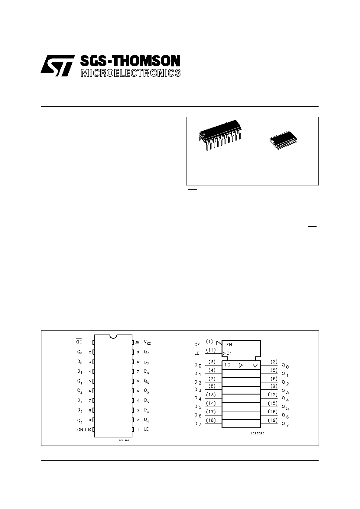
(Plastic Package)
(Micro Package)
M
ORDERCODES:
74AC373B 74AC373M
(OE).
While the LE inputs is held at a high level, the Q
outputs will follow the data input precisely or
inversely. When the LE is taken low, the Q
outputs will be latched precisely or inversely at
the logic level of D input data. While the (OE)
input is low, the 8 outputs will be in a normallogic
state (high or low logic level) and while high level
the outputs will be in a high impedance state.
This device is designed to interface directly High
Speed CMOS systems with TTL and NMOS
components.
All inputs and outputs are equipped with
protectioncircuits against static discharge, giving
them 2KV ESD immunity and transient excess
voltage.
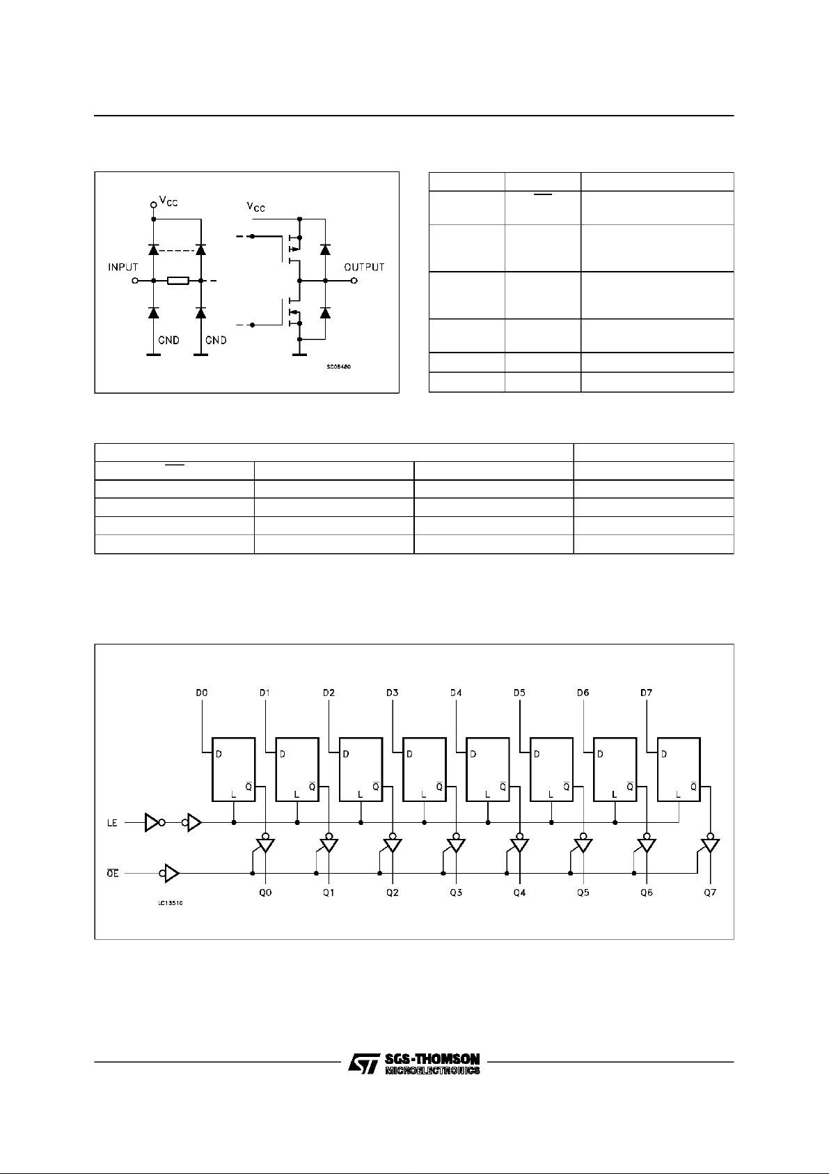
PINCONNECTION AND IEC LOGIC SYMBOLS
April 1997
1/10
Page 2
74AC373
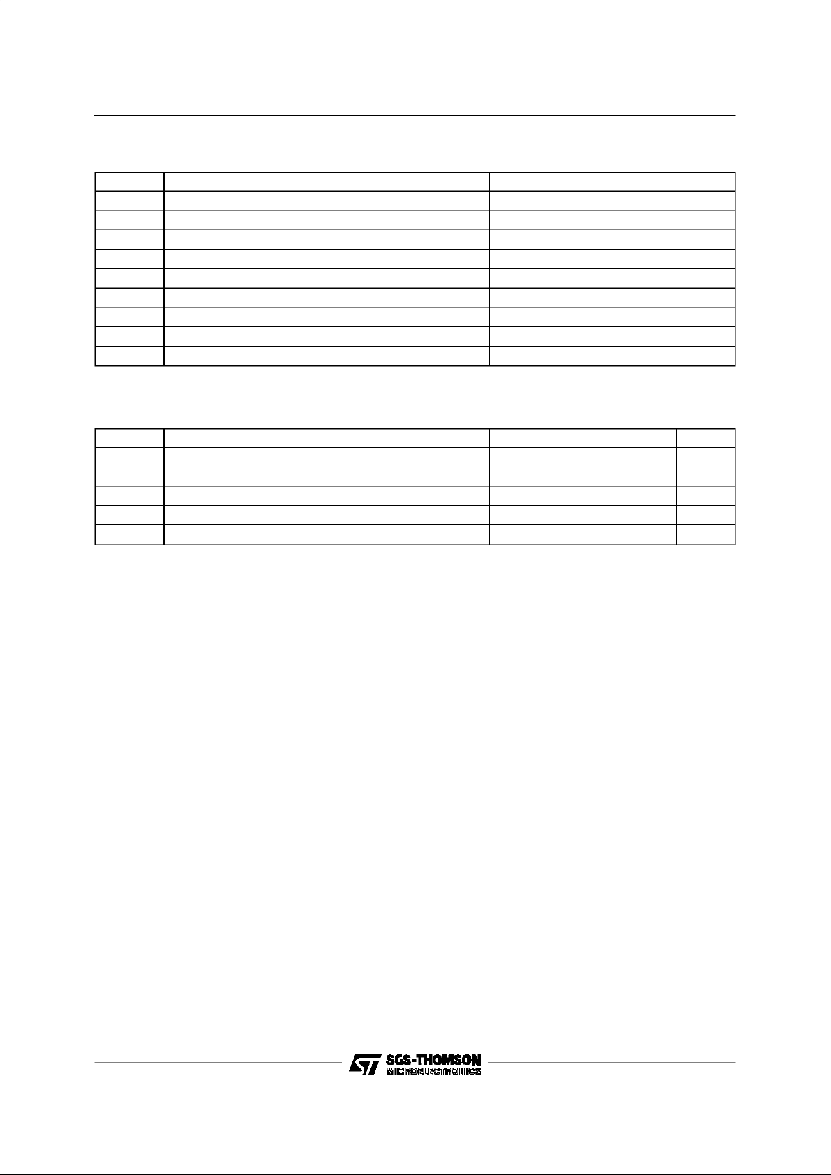
INPUTAND OUTPUTEQUIVALENTCIRCUIT PIN DESCRIPTION
PI N No SYM B O L NAME AN D FUNC T I ON
1 OE 3 State Output Enable
2, 5, 6,
9, 12, 15,
16, 19
3, 4, 7,
8, 13, 14,
17, 18
11 LE Latch Enable
10 GND Ground (0V)
20 V
TRUTH TABLE
INPUTS OUTPUTS
OE LE D Q
HXXZ
L L X NO CHANGE
LHLL
LHHH
X:DON’T CARE
Z:HIGHIMPEDANCE
*:Q OUTPUTS ARELATCHED AT THE TIMEWHENTHEINPUT IS TAKEN LO W LOG ICLEVEL.
Q0 to Q7 Data Inputs
D0 to D7 3 State Outputs
CC
Input (Active LOW)
Input
Positive Supply Voltage
LOGICDIAGRAMS
2/10
Page 3
74AC373
ABSOLUTE MAXIMUM RATINGS
Symb o l Parameter Val u e Uni t
V
V
V
I
I
OK
I
orI
I
CC
T
T
Absolute Maximum Ratings are those values beyond which damage to the device may occur. Functional operation under these condition is not implied.
RECOMMENDEDOPERATINGCONDITIONS
Symb o l Parameter Value Un i t
V
V
V
T
dt/dv Input Rise and Fall Time V
1) VINfrom30%to 70%of V
Supply Voltage -0.5 to +7 V
CC
DC Input Voltage -0.5 to VCC+ 0.5 V
I
DC Output Voltage -0.5 to VCC+ 0.5 V
O
DC Input Diode Current ± 20 mA
IK
DC Output Diode Current ± 20 mA
DC Output Current ± 50 mA
O
DC VCCor Ground Current ± 400 mA
GND
Storage Temperature -65 to +150
stg
Lead Temperature (10 sec) 300
L
Supply Voltage 2 to 6 V
CC
Input Voltage 0 to V
I
Output Voltage 0 to V
O
Operating Temperature: -40 to +85
op
= 3.0, 4.5 or 5.5 V(note 1) 8 ns/V
CC
CC
CC
CC
o
C
o
C
V
V
o
C
3/10
Page 4

74AC373
DC SPECIFICATIONS
Symbol Parameter Test Condit ions Value Unit
V
CC
(V)
High Level Input Voltage 3.0 VO= 0.1 V or
V
IH
4.5 3.15 2.25 3.15
V
CC
- 0.1 V
T
=25oC-40to85
A
Min. Typ. Max. Min . Max.
2.1 1.5 2.1
o
C
5.5 3.85 2.75 3.85
Low Level Input Voltage 3.0 VO= 0.1 V or
V
IL
4.5 2.25 1.35 1.35
V
CC
- 0.1 V
1.5 0.9 0.9
5.5 2.75 1.65 1.65
High Level Output
V
OH
Voltage
Low Level Output
V
OL
Voltage
Input Leakage Current
I
I
3-State Output Off-state
I
OZ
Current
Quiescent Supply
I
CC
3.0
4.5 I
5.5 I
V
V
3.0 I
4.5 I
5.5 I
3.0
4.5 I
5.5 I
V
V
3.0 I
4.5 I
5.5 I
5.5
5.5 VI=VCCor GND
V
IO=-50 µA 2.9 2.99 2.9
(*)
I
IH
V
IL
=-50 µA 4.4 4.49 4.4
O
=
=-50 µA 5.4 5.49 5.4
or
O
=-12 mA 2.56 2.46
O
=-24 mA 3.86 3.76
O
=-24 mA 4.86 4.76
O
IO=50 µA 0.002 0.1 0.1
(*)
I
IH
V
IL
=50 µA 0.001 0.1 0.1
O
=
=50 µA 0.001 0.1 0.1
or
O
=12 mA 0.36 0.44
O
=24 mA 0.36 0.44
O
=24 mA 0.36 0.44
O
VI=VCCor GND ±0.1 ±1 µA
±0.5 ±5 µA
V
I(OE)=VIH
or GND
O=VCC
5.5 VI=VCCor GND 8 80 µA
Current
Dynamic Output Current
I
OLD
OHD
(note 1, 2)
I
1) Maximum test duration 2ms, one output loaded at time
2) Incident wave switching is guaranteed on transmission lines with impedances as low as 50 Ω.
(*)All outputs loaded.
5.5 V
= 1.65 V max 75 mA
OLD
V
= 3.85 V min -75 mA
OHD
V
V
V
V
4/10
Page 5

AC ELECTRICAL CHARACTERISTICS (CL= 50 pF, RL=500 Ω, Inputtr=tf=3ns)
74AC373
Symbol Parameter Test Cond itio n Value Unit
o
C
ns
ns
ns
ns
ns
ns
ns
t
Propagation Delay Time
PLH
t
LE to Q
PHL
Propagation Delay Time
t
PLH
t
DtoQ
PHL
Output EnableTime 3.3
t
PZL
t
PZH
Output Disable Time 3.3
t
PLZ
t
PHZ
t
Clock Pulse Width HIGH
w
or LOW
Setup Time Q to CK
t
s
HIGH or LOW
Hold Time Q to CK
t
h
HIGH or LOW
(*) Voltagerange is3.3V± 0.3V
(**) Voltagerangeis5V± 0.5V
V
3.3
5.0
3.3
5.0
5.0
5.0
3.3
5.0
3.3
5.0
3.3
5.0
(V)
CC
(**)
(**)
(**)
(**)
(**)
(**)
(**)
T
=25oC-40to85
A
Min. Typ. Max. Min . Max.
(*)
6.5 12.0 14.0
5.0 9.5 10.5
(*)
6.5 12.0 14.0
5.0 9.5 10.5
(*)
7.0 11.0 13.0
5.0 8.5 9.5
(*)
7.5 12.0 13.0
6.5 9.0 10.0
(*)
1.5 5.5 6.0
1.5 4.0 4.5
(*)
0.5 5.5 6.0
0.5 4.0 4.5
(*)
-0.5 1.0 5.0
-0.5 1.0 5.0
CAPACITIVE CHARACTERISTICS
Symbol Parameter Test Condit ions Value Unit
T
V
CC
(V)
C
Output Capacitance
OUT
Input Capacitance
C
IN
Power Dissipation
C
PD
5.0
5.0
5.0 20 pF
=25oC-40to85
A
Min. Typ. Max. Min . Max.
8
4
Capacitance (note 1)
1) CPDis defined as the value of the IC’s internal equivalent capacitance which is calculated from the operating current consumption without load. (Refer to
Test Circuit). Average operating current can be obtained by the following equation. I
(opr) =CPD• VCC•fIN+ICC/n (percircuit)
CC
o
C
pF
pF
5/10
Page 6

74AC373
TEST CIRCUIT
TEST SWITCH
t
PLH,tPHL
t
PZL,tPLZ
t
PZH,tPHZ
CL= 50 pF or equivalent (includes jig and probe capacitance)
= 500Ω or equivalent
R
L=R1
R
of pulse generator (typically 50Ω)
T=ZOUT
Open
2V
CC
Open
WAVEFORM 1: LE TO Qn PROPAGATION DELAYS, LE MINIMUM PULSE WIDTH,
Dn TOLE SETUPAND HOLD TIMES (f=1MHz;50% duty cycle)
6/10
Page 7

WAVEFORM 2: OUTPUT ENABLE AND DISABLE TIMES (f=1MHz; 50% duty cycle)
74AC373
WAVEFORM 3: PROPAGATIONDELAY TIME (f=1MHz; 50% duty cycle)
7/10
Page 8

74AC373
Plastic DIP20 (0.25) MECHANICAL DATA
DIM.
MIN. TYP. MAX. MIN. TYP. MAX.
a1 0.254 0.010
B 1.39 1.65 0.055 0.065
b 0.45 0.018
b1 0.25 0.010
D 25.4 1.000
E 8.5 0.335
e 2.54 0.100
e3 22.86 0.900
F 7.1 0.280
I 3.93 0.155
L 3.3 0.130
Z 1.34 0.053
mm inch
8/10
P001J
Page 9

SO20 MECHANICAL DATA
74AC373
DIM.
MIN. TYP. MAX. MIN. TYP. MAX.
A 2.65 0.104
a1 0.10 0.20 0.004 0.007
a2 2.45 0.096
b 0.35 0.49 0.013 0.019
b1 0.23 0.32 0.009 0.012
C 0.50 0.020
c1 45° (typ.)
D 12.60 13.00 0.496 0.512
E 10.00 10.65 0.393 0.419
e 1.27 0.050
e3 11.43 0.450
F 7.40 7.60 0.291 0.299
L 0.50 1.27 0.19 0.050
M 0.75 0.029
S8°(max.)
mm inch
P013L
9/10
Page 10

74AC373
Information furnished is believed to be accurateandreliable.However,SGS-THOMSON Microelectronicsassumesno responsability for the
consequencesof use ofsuch informationnor for any infringement of patents or otherrights of third parties which may resultsfrom its use. No
licenseisgrantedby implicationor otherwise underany patentorpatent rightsofSGS-THOMSONMicroelectronics.Specificationsmentioned
in this publicationare subjecttochange withoutnotice.This publication supersedes and replaces all informationpreviously supplied.
SGS-THOMSONMicroelectronics productsare notauthorized for useas criticalcomponents in lifesupportdevicesor systemswithoutexpress
writtenapproval of SGS-THOMSON Microelectonics.
1997 SGS-THOMSONMicroelectronics- Printedin Italy - All Rights Reserved
Australia- Brazil - Canada - China- France- Germany - Hong Kong- Italy- Japan- Korea- Malaysia- Malta - Morocco- TheNetherlands-
Singapore- Spain- Sweden- Switzerland-Taiwan- Thailand - United Kingdom - U.S.A
SGS-THOMSONMicroelectronics GROUPOF COMPANIES
.
10/10
 Loading...