

Page 1
74AC32
QUAD 2-INPUT OR GATE
■ HIGH SPEED: t
■ LOW POWER DISSIPATION:
= 2µA(MAX.) at TA=25°C
I
CC
■ HIGH NOISE IMMUNITY:
V
= V
NIH
■ 50Ω TRANSMISSION LINE DRIVING
= 28 % VCC (MIN.)
NIL
= 4ns (TYP.) at VCC = 5V
PD
CAPABILITY
■ SYMMETRICAL OUTPUT IMPEDANCE:
|I
| = IOL = 24mA (MIN)
OH
■ BALANCED PROPAGATION DELAYS:
t
≅ t
PLH
■ OPERATING VOLTAGE RANGE:
V
CC
■ PIN AND FUNCTION COMPATIBLE WITH
PHL
(OPR) = 2V to 6V
74 SERIES 32
■ IMPROVED LATCH-UP IMMUNITY
DESCRIPTION
The 74AC32 is an advanced high-speed CMOS
QUAD 2-INPUT OR GATE fabricated with
sub-micron silicon gate and double-layer metal
wiring C
2
MOS tecnology.
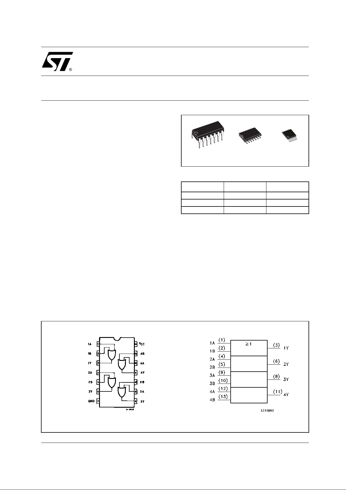
TSSOPDIP SOP
ORDER CODES
PACKAGE TUBE T & R
DIP 74AC32B
SOP 74AC32M 74AC32MTR
TSSOP 74AC32TTR
The internal circuit is composed of 2 stages
including buffer output , which enables high noise
immunity and stable output.
All inputs and outputs are equipped with
protection circuits against stat ic discharge, giving
them 2KV ESD immunity and transient excess
voltage.
PIN CONNECTION AND IEC LOGIC SYMBOLS
1/8April 2001
Page 2
74AC32
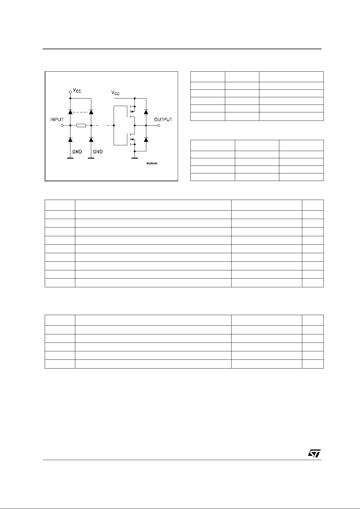
INPUT AND OUTPUT EQUIVALENT CIRCUIT PIN DESCRIPTION
PIN No SYMBOL NAME AND FUNCTION
1, 4, 9, 12 1A to 4A Data Inputs
2, 5, 10, 13 1B to 4B Data Inputs
3, 6, 8, 11 1Y to 4Y Data Outputs
7 GND Ground (0V)
14
V
CC
TRUTH TABLE
ABY
LLL
LHH
HLH
HHH
ABSOLUTE MAXIMUM RATINGS
Symbol Parameter Value Unit
V
V
V
I
I
OK
I
I
or I
CC
T
T
Absolute Maximum Ratings are those values beyond which damage to the device may occur. Functional operation under these conditions is
not impl ied.
Supply Voltage
CC
DC Input Voltage -0.5 to VCC + 0.5
I
DC Output Voltage -0.5 to VCC + 0.5
O
DC Input Diode Current
IK
DC Output Diode Current
DC Output Current
O
DC VCC or Ground Current
GND
Storage Temperature
stg
Lead Temperature (10 sec)
L
Positive Supply Voltage
-0.5 to +7 V
V
V
± 20 mA
± 20 mA
± 50 mA
± 200 mA
-65 to +150 °C
300 °C
RECOMMENDED OPERATING CONDITIONS
Symbol Parameter Value Unit
V
V
V
T
dt/dv
1) VIN from 30% to 70% of V
2/8
Supply Voltage
CC
Input Voltage 0 to V
I
Output Voltage 0 to V
O
Operating Temperature
op
Input Rise and Fall Time V
CC
= 3.0, 4.5 or 5.5V (note 1)
CC
2 to 6 V
CC
CC
-55 to 125 °C
8 ns/V
V
V
Page 3
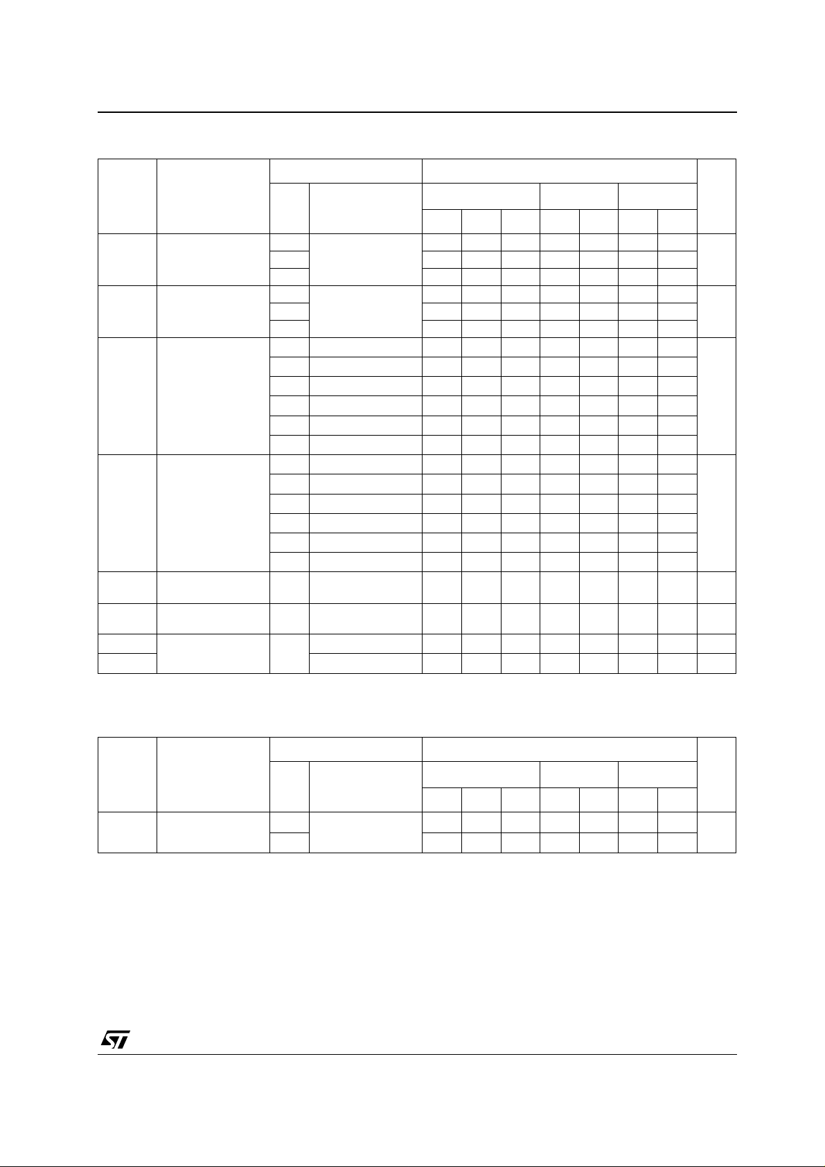
DC SPECIFICATIONS
Test Condition Value
= 25°C
Symbol Parameter
V
CC
(V)
V
V
V
V
I
I
OLD
I
OHD
1) Maxim um test duration 2ms, one output loaded at time
2) Incid ent wave swi tc hi ng is guara nt eed on transmi ssion line s wi t h i mpedance s as low as 50Ω
High Level Input
IH
Voltage
Low Level Input
IL
Voltage
High Level Output
OH
Voltage
Low Level Output
OL
Voltage
I
Input Leakage
I
Current
Quiescent Supply
CC
Current
Dynamic Output
Current (note 1, 2)
3.0
5.5 3.85 2.75 3.85 3.85
3.0
5.5 2.75 1.65 1.65 1.65
3.0
4.5
5.5
3.0
4.5
5.5
3.0
4.5
5.5
3.0
4.5
5.5
5.5
5.5
5.5
= 0.1 V or
V
O
V
-0.1V
CC
= 0.1 V or
V
O
V
-0.1V
CC
=-50 µA
I
O
I
=-50 µA
O
I
=-50 µA
O
I
=-12 mA
O
I
=-24 mA
O
I
=-24 mA
O
IO=50 µA
I
=50 µA
O
I
=50 µA
O
I
=12 mA
O
I
=24 mA
O
I
=24 mA
O
= VCC or GND
V
I
= VCC or GND
V
I
V
= 1.65 V max
OLD
V
= 3.85 V min
OHD
T
A
Min. Typ. Max. Min. Max. Min. Max.
2.1 1.5 2.1 2.1
1.5 0.9 0.9 0.9
2.9 2.99 2.9 2.9
4.4 4.49 4.4 4.4
5.4 5.49 5.4 5.4
2.56 2.46 2.4
3.86 3.76 3.7
4.86 4.76 4.7
0.002 0.1 0.1 0.1
0.001 0.1 0.1 0.1
0.001 0.1 0.1 0.1
0.36 0.44 0.5
0.36 0.44 0.5
0.36 0.44 0.5
± 0.1 ± 1 ± 1 µA
22040µA
74AC32
-40 to 85°C -55 to 125°C
75 50 mA
-75 -50 mA
Unit
V4.5 3.15 2.25 3.15 3.15
V4.5 2.25 1.35 1.35 1.35
V
V
AC ELECTRICAL CHARACTERISTICS (CL = 50 pF, RL = 500 Ω, Input tr = tf = 3ns)
Test Condition Value
= 25°C
Symbol Parameter
t
PLH tPHL
(*) Vol tage range is 3. 3V ± 0.3V
(**) Voltage range is 5.0V ±
Propagation Delay
Time
0.5V
V
3.3
5.0
CC
(V)
(*)
(**)
T
A
-40 to 85°C -55 to 125°C
Min. Typ. Max. Min. Max. Min. Max.
1.5 5.5 9.0 1.0 10.0 1.0 12.0
1.5 4.0 7.5 1.0 8.5 1.0 9.0
Unit
ns
3/8
Page 4

74AC32
CAPACITIVE CHARACTERISTICS
Test Condition Value
T
Symbol Parameter
C
C
Input Capacitance
IN
Power Dissipation
PD
Capacitance
V
CC
(V)
5.0 4 pF
5.0
= 10MHz
f
IN
= 25°C
A
Min. Typ. Max. Min. Max. Min. Max.
33 pF
(note 1)
1) CPD is defined as the value of the IC’s internal equivalent capacitance which is calculated from the operating current consumption without
load. (Refer to Test Circuit). Average operating current can be obtained by the following equation. I
TEST CIRCUIT
-40 to 85°C -55 to 125°C
= CPD x VCC x fIN + ICC/4 (per gate)
CC(opr)
Unit
CL = 50pF or equivalent (includes jig and p robe capacit ance)
= R1 = 500Ω or equivalent
R
L
R
= Z
of pulse generator (typically 50Ω)
T
OUT
WAVEFORM: PROPAGATION DELAYS (f=1MHz; 50% duty cycle)
4/8
Page 5

Plastic DIP-14 MECHANICAL DATA
74AC32
DIM.
MIN. TYP. MAX. MIN. TYP. MAX.
a1 0.51 0.020
B 1.39 1.65 0.055 0.065
b0.5 0.020
b1 0.25 0.010
D200.787
E8.5 0.335
e2.54 0.100
e3 15.24 0.600
F7.10.280
I5.10.201
L3.3 0.130
Z 1.27 2.54 0.050 0.100
mm inch
P001A
5/8
Page 6

74AC32
SO-14 MECHANICAL DATA
DIM.
MIN. TYP. MAX. MIN. TYP. MAX.
A1.750.068
a1 0.1 0.2 0.003 0.007
a2 1.65 0.064
b 0.35 0.46 0.013 0.018
b1 0.19 0.25 0.007 0.010
C0.5 0.019
c1 45 (typ.)
D 8.55 8.75 0.336 0.344
E 5.8 6.2 0.228 0.244
e1.27 0.050
e3 7.62 0.300
F 3.8 4.0 0.149 0.157
G 4.6 5.3 0.181 0.208
L 0.5 1.27 0.019 0.050
M0.680.026
S8 (max.)
mm inch
6/8
P013G
Page 7

TSSOP14 MECHANICAL DATA
74AC32
DIM.
mm inch
MIN. TYP. MAX. MIN. TYP. MAX.
A1.10.433
A1 0.05 0.10 0.15 0.002 0.004 0.006
A2 0.85 0.9 0.95 0.335 0.354 0.374
b 0.19 0.30 0.0075 0.0118
c 0.09 0.20 0.0035 0.0079
D 4.9 5 5.1 0.193 0.197 0.201
E 6.25 6.4 6.5 0.246 0.252 0.256
E1 4.3 4.4 4.48 0.169 0.173 0.176
e 0.65 BSC 0.0256 BSC
K0
o
o
4
o
8
o
0
o
4
o
8
L 0.50 0.60 0.70 0.020 0.024 0.028
A2
A
A1
PIN 1 IDENTIFICATION
b
e
c
K
L
E
D
E1
1
7/8
Page 8

74AC32
Information furnished is bel ieved to be accurate and reliable. However, STMicroe lectronics assumes no responsibility for the
consequences of use of such information nor for any infringement of patents or other rights of third parties which may result from
its use. No li cense is granted by imp lication or otherwise under a ny patent or patent rig hts of STMicroelectronics. Spec ific at ions
mentioned in this publication ar e subject to change without notice. This publication supersedes and replaces all information
previously supplied. S TMicroelectronics products are not authorized for use as critica l components in life suppo rt devices or
systems without express written approval of STMicroelectronics.
Australi a - Brazil - Chi na - Finland - F rance - Germany - Hong Kon g - I ndia - Italy - Japan - Malay sia - Malta - Morocco
© The ST logo is a registered trademark of STMicroelectronics
© 2001 STM icroelectronics - Printed in Ital y - All Rights Reserved
STMicr o el ectronics GROUP OF COMPANIES
Singapo re - Spain - Sweden - Switzerland - Uni ted Kingdom
© http://www.st.com
8/8
 Loading...