

Datasheet 74AC299SJX, 74AC299SJ, 74AC299SCX, 74AC299SC, 74AC299PC Datasheet (Fairchild Semiconductor)
...Page 1
© 1999 Fairchild Semiconductor Corporation DS009893 www.fairchildsemi.com
July 1988
Revised November 1999
74AC299 • 74ACT299 8-Input Universal Shift/Storage Register
74AC299 • 74ACT299
8-Input Universal Shift/Storage Register
with Common Parallel I/O Pins
General Description
The AC/ACT299 is a n 8-bit universa l shift/storag e register
with 3-STATE outputs. Four modes of operation a re possible: hold (store), shift left, shift right and load data. The parallel load inputs and flip-flop outputs are multiplexed to
reduce the total num ber of package pins. Additiona l outputs are provided for flip-flops Q
0
, Q7 to allow easy serial
cascading. A separate active LOW Master Reset is used to
reset the register.
Features
■ ICC and IOZ reduced by 5 0%
■ Common parallel I/O for reduced pin count
■ Additional serial inputs and outputs for expansion
■ Four operating modes: shift left, shift right, load
and store
■ 3-STATE outputs for bus-oriented applications
■ Outputs source/sink 24 mA
■ ACT299 has TTL-compatible inputs
Ordering Code:
Device also available in Tape and Reel. Specify by appending su ffix le tter “X” to the ordering code.
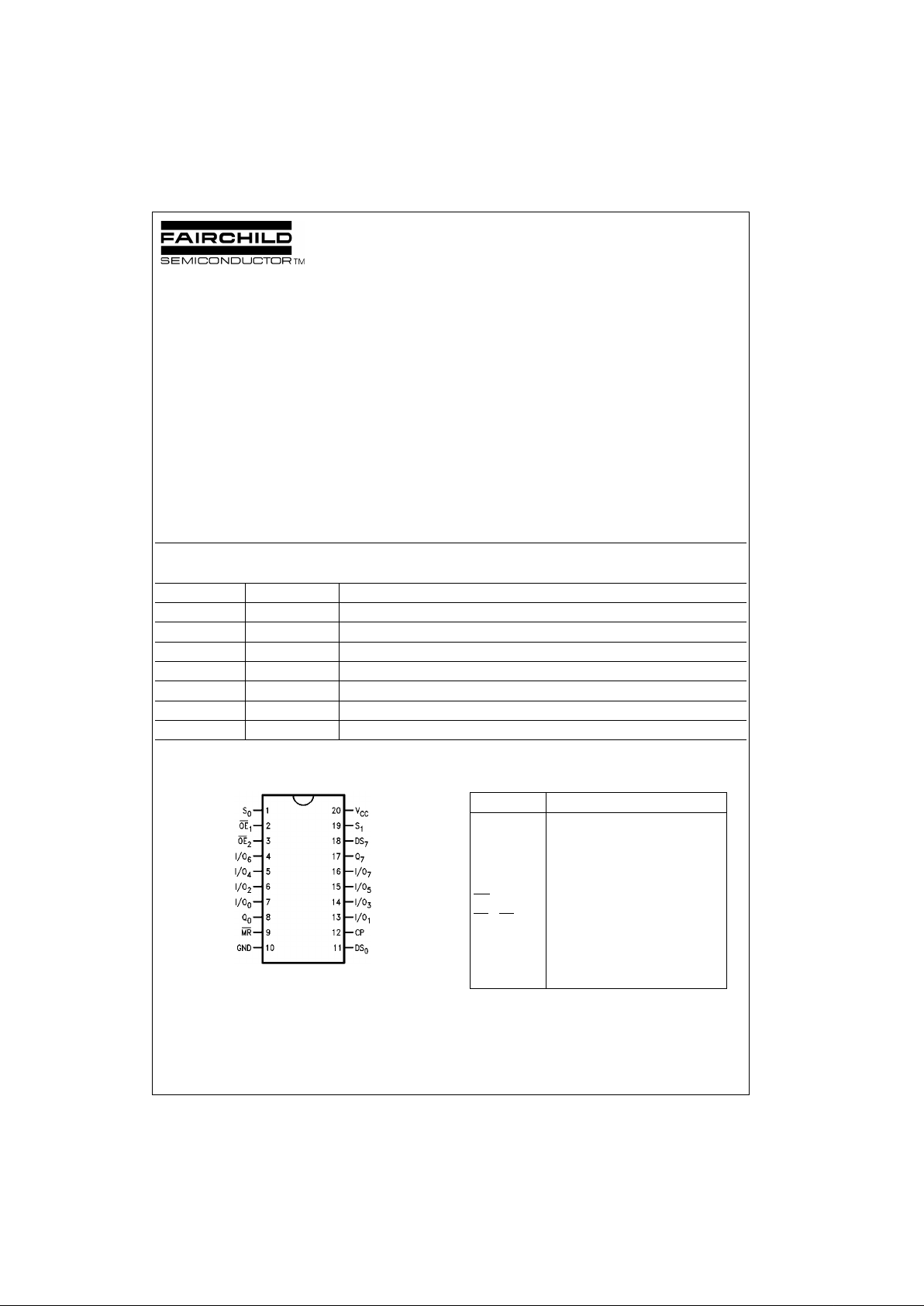
Connection Diagram Pin Descriptions
FACT is a trademark of Fairchild Semiconductor Corporation.
Order Number Package Number Package Description
74AC299SC M20B 20-Lead Small Outline Integrated Circuit (SOIC), JEDEC MS-013, 0.300” Wide Body
74AC299SJ M20D 20-Lead Small Outline Package (SOP), EIAJ TYPE II, 5.3mm Wide
74AC299MTC MTC20 20-Lead Thin Shrink Small Outline Package (TSSOP), JEDEC MO-153, 4.4mm Wide
74AC299PC N20A 20-Lead Plastic Dual-In-Line Package (PDIP), JEDEC MS-001, 0.300” Wide
74ACT299SC M20B 20-Lead Small Outline Integrated Circuit (SOIC), JEDEC MS-013, 0.300” Wide Body
74ACT299MTC MTC20 20-Lead Thin Shrink Small Outline Package (TSSOP), JEDEC MO-153, 4.4mm Wide
74ACT299PC N20A 20-Lead Plastic Dual-In-Line Package (PDIP), JEDEC MS-001, 0.300” Wide
Pin Names Description
CP Clock Pulse Input
DS
0
Serial Data Input for Right Shift
DS
7
Serial Data Input for Left Shift
S
0
, S
1
Mode Select Inputs
MR
Asynchronous Master Reset
OE
1
, OE
2
3-STATE Output Enable Inputs
I/O
0
–I/O
7
Parallel Data Inputs or
3-STATE Parallel Outputs
Q
0
, Q
7
Serial Outputs
Page 2
www.fairchildsemi.com 2
74AC299 • 74ACT299
Logic Symbols
IEEE/IEC
Tr uth Table
H = HIGH Voltage Level
L = LOW Voltage Level
X = Immaterial
= LOW-to-HIGH Transition
Functional Description
The AC/ACT299 contains eig ht edge-trigge red D-type flipflops and the interstage lo gic necessary to perform synchronous shift left, shift right, para llel lo ad an d hold operations. The type of operation is determined by S
0
and S1, as
shown in the Truth Table. All flip-flop outputs are br ought
out through 3-STATE buffers to separate I/O pins that also
serve as data inputs in th e parallel load mode. Q
0
and Q
7
are also brought out on other pin s for expansion in serial
shifting of longer words.
A LOW signal on MR
overrides the Select and CP inputs
and resets the flip-flops. All othe r state changes are initiated by the rising edge o f the clock. Inputs can change
when the clock is in either stat e provide d onl y that the r ecommended setup and hold times, relative to the rising edge
of CP, are observed.
A HIGH signal on either OE
1
or OE2 disables the 3-STATE
buffers and puts the I /O pins in the h igh impedance state.
In this condition the shift, hold, load a nd reset operations
can still occur. The 3-STATE buffers are also disabled by
HIGH signals on both S
0
and S1 in preparation for a par al-
lel load operation.
Inputs Response
MR S
1S0
CP
L X X X Asynchronous Reset; Q
0–Q7
= LOW
HHH
Parallel Load; I/On → Q
n
HLHShift Right; DS0 → Q0, Q0 → Q1, etc.
HHL
Shift Left, DS7 → Q7, Q7 → Q6, etc.
H L L X Hold
Page 3
3 www.fairchildsemi.com
74AC299 • 74ACT299
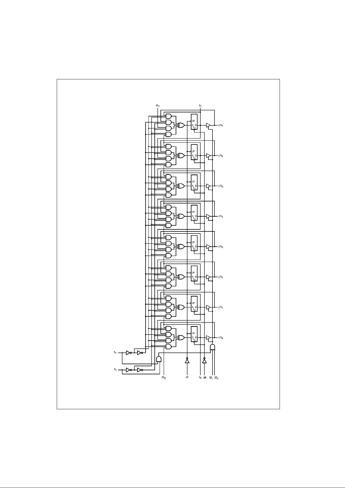
Logic Diagram
Please note that this diagram is provided only for the understanding of logic operations and should not be used to estimate propagation delays.
Page 4
www.fairchildsemi.com 4
74AC299 • 74ACT299
Absolute Maximum Ratings(Note 1) Recommended Operating
Conditions
Note 1: Absolute maximum ratings are those values beyond which damage
to the device may occur. Obviously the databook specifications should be
met, without exception, to ensure that the system design is reliable over its
power supply, temperature, an d output/input loading variables. Fairc hild
does not recommend operation of FACT circuits outside databook specifications.
DC Electrical Characteristics for AC
Supply Voltage (VCC) −0.5V to +7.0V
DC Input Diode Current (I
IK
)
V
I
= −0.5V −20 mA
V
I
= VCC +0.5V +20 mA
DC Input Voltage (V
I
) −0.5V to VCC +0.5V
DC Output Diode Current (I
OK
)
V
O
= −0.5V −20 mA
V
O
= VCC +0.5V +20 mA
DC Output Voltage (V
O
) −0.5V to VCC +0.5V
DC Output Source or Sink Current (I
O
) ± 50 mA
DC V
CC
or Ground Current
Per Output Pin (I
CC
or I
GND
) ± 50 mA
Storage Temperature (T
STG
) −65°C to +150°C
Junction Temperature (T
J
)
(PDIP) 140°C
Supply Voltage (V
CC
)
(Unless Otherwise Specified)
AC 2.0V to 6.0V
ACT 4.5V to 5.0V
Input Voltage (V
I
) 0V to V
CC
Output Voltage (VO) 0V to V
CC
Operating Temperature (TA) −40°C to +85°C
Minimum Input Edge Rate (∆V/∆t)
AC Devices
V
IN
from 30% to 70% of V
CC
VCC @ 3.3V, 4.5V, 5.5V 125 mV/ns
Minimum Input Edge Rate (∆V/∆t)
ACT Devices
V
IN
from 0.8V to 2.0V
V
CC
@ 4.5V, 5.5V 125 mV/ns
Symbol Parameter
V
CC
TA = 25°CT
A
= −40°C to +85°C
Units Conditions
(V) Typ Guaranteed Limits
V
IH
Minimum HIGH Level 3.0 1.5 2.1 2.1 V
OUT
= 0.1V
Input Voltage 4.5 2.25 3.15 3.15 V or VCC − 0.1V
5.5 2.75 3.85 3.85
V
IL
Maximum LOW Level 3.0 1.5 0.9 0.9 V
OUT
= 0.1V
Input Voltage 4.5 2.25 1.35 1.35 V or VCC − 0.1V
5.5 2.75 1.65 1.65
V
OH
Minimum HIGH Level 3.0 2.99 2.9 2.9
Output Voltage 4.5 4.49 4.4 4.4 V I
OUT
= −50 µA
5.5 5.49 5.4 5.4
VIN = VIL or V
IH
3.0 2.56 2.46 V IOH = −12 mA
4.5 3.86 3.76 IOH = −24 mA
5.5 4.86 4.76 IOH = −24 mA (Note 2)
V
OL
Maximum LOW Level 3.0 0.002 0.1 0.1
Output Voltage 4.5 0.001 0.1 0.1 V I
OUT
= 50 µA
5.5 0.001 0.1 0.1
VIN = VIL or V
IH
3.0 0.36 0.44 IOH = 12 mA
4.5 0.36 0.44 V IOH = 24 mA
5.5 0.36 0.44 IOH = 24 mA (Note 2)
I
IN
Maximum Input
5.5 ± 0.1 ± 1.0 µA
VI = VCC, GND
(Note 4) Leakage Current
I
OLD
Minimum Dynamic 5.5 86 mA V
OLD
= 1.65V Max
I
OHD
Output Current (Note 3) −75 mA V
OHD
= 3.85V Min
I
CC
(Note 4) Maximum Quiescent
5.5 4.0 40.0 µAVIN = VCC or GND
Supply Current
Page 5

5 www.fairchildsemi.com
74AC299 • 74ACT299
DC Electrical Characteristics for AC (Continued)
Note 2: All outputs loaded; threshold on input associated with output under test.
Note 3: Maximum test duration 20 ms, one output loaded at a time.
Note 4: I
IN
and ICC @ 3.0V are guaranteed to be less than or equa l t o th e respective limit @ 5.5V VCC.
DC Electrical Characteristics for ACT
Note 5: All outputs loaded; thres holds on input associate d w it h output under test.
Note 6: Maximum test duration 2.0 ms, one output loaded at a time.
Symbol Parameter
V
CC
TA = 25°CTA = −40°C to +85°C
Units Conditions
(V) Typ Guaranteed Limits
I
OZT
Maximum I/O Leakage Current
5.5 ± 0.3 ± 3.0 µA
VI (OE) = VIL, V
IH
VI = VCC, GND
V
O
= VCC, GND
Symbol Parameter
V
CC
TA = 25°CTA = −40°C to +85°C
Units Conditions
(V) Typ Guaranteed Limits
V
IH
Minimum HIGH Level 4.5 1.5 2.0 2.0
V
V
OUT
= 0.1V
Input Voltage 5.5 1.5 2.0 2.0 or VCC − 0.1V
V
IL
Maximum LOW Level 3.0 1.5 0.8 0.8
V
V
OUT
= 0.1V
Input Voltage 4.5 1.5 0.8 0.8 or V
CC
− 0.1V
V
OH
Minimum HIGH Level 4.5 4.49 4.4 4.4
VI
OUT
= −50 µA
5.5 5.49 5.4 5.4
VIN = VIL or V
IH
4.5 0.0001 3.86 3.76 V IOH = −24 mA
5.5 4.86 4.76 I
OH
= −24 mA (Note 5)
V
OL
Maximum LOW Level 4.5 0.001 0.1 0.1
VI
OUT
= 50 µA
Output Voltage 5.5 0.001 0.1 0.1
VIN = VIL or V
IH
4.5 0.36 0.44 V IOL= 24 mA
5.5 0.36 0.44 IOL= 24 mA (Note 5)
I
IN
Maximum Input Leakage Current 5.5 ± 0.1 ± 1.0 µAVI = VCC, GND
I
CCT
Maximum ICC/Input 5.5 0.6 1.5 mA VI = VCC − 2.1V
I
OLD
Minimum Dynamic 5.5 75 mA V
OLD
= 1.65V Max
I
OHD
Output Current (Note 6) 5.5 −75 mA V
OHD
= 3.85V Min
I
CC
Maximum Quiescent Supply Current 5.5 4.0 40.0 µAVIN = VCC or GND
I
OZT
Maximum I/O VI (OE) = VIL, V
IH
Leakage Current 5.5 ±0.3 ±3.0 µAVI = VCC, GND
V
O
= VCC, GND
Page 6

www.fairchildsemi.com 6
74AC299 • 74ACT299
AC Electrical Characteristics for AC
Note 7: Voltage Range 3.3 is 3.3V ± 0.3V.
Voltage Range 5.0 is 5.0V ± 0.5V.
AC Operating Requirements for AC
Note 8: Voltage Range 3.3 is 3.3V ± 0.3V
Voltage Range 5.0 is 5.0V ± 0.5V
V
CC
TA = +25°CT
A
= −40°C to +85°C
Symbol Parameter (V)
C
L
= 50 pF CL = 50 pF
Units
(Note 7) Min Typ Max Min Max
f
MAX
Maximum Input 3.3 90 124 80
MHz
Frequency 5.0 130 173 105
t
PLH
Propagation Delay 3.3 8.5 14.0 20.5 7.0 22.0
ns
CP to Q
0
or Q7 (Shift Left or Right) 5.0 5.5 9.5 14.0 4.5 15.0
t
PHL
Propagation Delay 3.3 8.5 14.5 21.5 7.0 23.0
ns
CP to Q0 or Q7 (Shift Left or Right) 5.0 5.5 10.0 14.5 5.0 16.0
t
PLH
Propagation Delay 3.3 9.0 14.5 20.5 7.5 22.5
ns
CP
to I/O
n
5.0 6.0 10.0 14.5 5.0 16.0
t
PHL
Propagation Delay 3.3 10.0 16.0 23.0 8.5 24.5
ns
CP
to I/O
n
5.0 6.5 11.0 16.0 6.0 17.5
t
PHL
Propagation Delay 3.3 9.0 15.5 22.5 7.5 25.0
ns
MR to Q0 or Q
7
5.0 5.5 10.5 15.5 5.0 17.0
t
PHL
Propagation Delay 3.3 9.0 15.0 21.5 7.5 24.0
ns
MR
to I/O
n
5.0 5.5 10.0 15.0 5.0 16.5
t
PZH
Output Enable Time 3.3 7.0 12.0 18.0 6.0 19.5
ns
OE
to I/O
n
5.0 4.5 8.5 12.5 4.0 13.5
t
PZL
Output Enable Time 3.3 7.0 12.5 18.0 6.0 20.5
ns
OE to I/O
n
5.0 5.0 8.0 12.5 4.0 14.0
t
PHZ
Output Disable Time 3.3 6.5 13.0 18.5 5.5 19.5
ns
OE
to I/O
n
5.0 3.5 9.5 14.0 3.0 15.0
t
PLZ
Output Disable Time 3.3 5.5 11.5 17.0 4.5 19.0
ns
OE
to I/O
n
5.0 3.5 8.0 12.5 2.0 13.5
V
CC
TA = +25°CT
A
= −40°C to +85°C
Symbol Parameter (V)
C
L
= 50 pF CL = 50 pF
Units
(Note 8) Typ Guaranteed Minimum
t
S
Setup Time, HIGH or LOW 3.3 3.0 8.0 8.5
ns
S0 or S1 to CP 5.0 2.0 5.0 5.5
t
H
Hold Time, HIGH or LOW 3.3 −3.0 0.5 0.5
ns
S
0
or S1 to CP 5.0 −1.5 1.0 1.0
t
S
Setup Time, HIGH or LOW 3.3 2.0 5.5 6.0
ns
I/On to CP 5.0 1.0 3.5 4.0
t
H
Hold Time, HIGH or LOW 3.3 −2.0 0 0
ns
I/On to CP 5.0 −1.0 1.0 1.0
t
S
Setup Time, HIGH or LOW 3.3 2.5 6.5 7.0
ns
DS0 or DS7 to CP 5.0 1.5 4.0 4.5
t
H
Hold Time, HIGH or LOW 3.3 −2.0 0 0.5
ns
DS0 or DS7 to CP 5.0 −1.0 1.0 1.0
t
W
CP Pulse Width, LOW 3.3 3.5 4.5 5.0
ns
5.0 2.0 3.5 3.5
t
W
MR Pulse Width, LOW 3.3 4.0 4.5 5.0
ns
5.0 2.0 3.5 3.5
t
REC
Recovery Time 3.3 0 1.5 1.5
ns
MR to CP 5.0 0.5 1.5 1.5
Page 7

7 www.fairchildsemi.com
74AC299 • 74ACT299
AC Electrical Characteristics for ACT
Note 9: Voltage Range 5.0 is 5.0V ± 0.5V
AC Operating Requirements for ACT
Note 10: Voltage Ran ge 5.0 is 5.0V ± 0.5V.
Capacitance
V
CC
TA = +25°CT
A
= −40°C to +85°C
Symbol Parameter (V)
C
L
= 50 pF CL = 50 pF
Units
(Note 9) Min Typ Max Min Max
f
MAX
Maximum Input Frequency 5.0 120 170 110 MHz
t
PLH
Propagation Delay
5.0 4.0 8.5 12.5 3.0 14.0 ns
CP to Q0 or Q7 (Shift Left or Right)
t
PHL
Propagation Delay
5.0 4.0 9.0 13.5 3.5 15.0 ns
CP to Q
0
or Q7 (Shift Left or Right)
t
PLH
Propagation Delay
5.0 4.5 8.5 12.5 4.5 13.5 ns
CP to I/O
n
t
PHL
Propagation Delay
5.0 5.0 9.5 15.0 4.5 16.5 ns
CP to I/O
n
t
PHL
Propagation Delay
5.0 4.0 14.0 15.0 4.0 18.0 ns
MR
to Q0 or Q
7
t
PHL
Propagation Delay
5.0 4.0 13.0 14.5 3.5 17.5 ns
MR
to I/O
n
t
PZH
Output Enable Time
5.0 2.5 8.0 12.0 1.5 13.0 ns
OE to I/O
n
t
PZL
Output Enable Time
5.0 2.0 8.0 12.0 1.5 13.5 ns
OE
to I/O
n
t
PHZ
Output Disable Time
5.0 2.0 8.5 12.5 2.0 13.5 ns
OE
to I/O
n
t
PLZ
Output Disable Time
5.0 2.5 8.0 11.5 2.0 12.5 ns
OE to I/O
n
V
CC
TA = +25°CT
A
= −40°C to +85°C
Symbol Parameter (V)
CL = 50 pF CL = 50 pF
Units
(Note 10) Typ Guaranteed Minimum
t
S
Setup Time, HIGH or LOW
5.0 2.0 5.0 5.5 ns
S
0
or S1 to CP
t
H
Hold Time, HIGH or LOW
5.0 −2.0 1.0 1.0 ns
S0 or S1 to CP
t
S
Setup Time, HIGH or LOW
5.0 1.5 4.0 4.5 ns
I/O
n
to CP
t
H
Hold Time, HIGH or LOW
5.0 −1.0 1.0 1.0 ns
I/O
n
to CP
t
S
Setup Time, HIGH or LOW
5.0 1.5 4.5 5.0 ns
DS0 or DS7 to CP
t
H
Hold Time, HIGH or LOW
5.0 −1.0 1.0 1.0 ns
DS0 or DS7 to CP
t
W
CP Pulse Width
5.0 2.0 4.0 4.5 ns
HIGH or LOW
t
W
MR Pulse Width, LOW 5.0 2.0 3.5 3.5 ns
t
REC
Recovery Time, MR to CP 5.0 0 1.5 1.5 ns
Symbol Parameter Typ Units Conditions
C
IN
Input Capacitance 4.5 pF VCC = 5.0V
C
PD
Power Dissipation Capacitance 170 pF VCC = 5.5V
Page 8

www.fairchildsemi.com 8
74AC299 • 74ACT299
Physical Dimensions inches (millimeters) unless otherwise noted
20-Lead Small Outline In tegrated Circuit (SOIC), JEDEC MS-013, 0.300” Wide Body
Package Number M20B
Page 9

9 www.fairchildsemi.com
74AC299 • 74ACT299
Physical Dimensions inches (millimeters) unless otherwise noted (Continued)
20-Lead Small Outline Package (SOP), EIAJ TYPE II, 5.3mm Wide
Package Number M20D
Page 10

www.fairchildsemi.com 10
74AC299 • 74ACT299
Physical Dimensions inches (millimeters) unless otherwise noted (Continued)
20-Lead Thin Shrink Small Outline Package (TSSOP), JEDEC MO-153, 4.4mm Wide
Package Number MTC20
Page 11

11 www.fairchildsemi.com
74AC299 • 74ACT299 8-Input Universal Shift/Storage Register
Physical Dimensions inches (millimeters) unless otherwise noted (Continued)
20-Lead Plastic Dual-In-Line Package (PDIP), JEDEC MS-001, 0.300” Wide
Package Number N20A
Fairchild does not assume any responsibility for use of any circuitry described , no circuit patent licenses are implied and
Fairchild reserves the right at any time without notice to change said circuitry and specifications.
LIFE SUPPORT POLICY
FAIRCHILD’S PRODUCTS ARE NOT AUTHORIZED FOR USE AS CRITICAL COMPONENTS IN LIFE SUPPORT
DEVICES OR SYSTEMS WITHOUT THE EXPRESS WRITTEN APPROVAL OF THE PRESIDENT OF FAIRCHILD
SEMICONDUCTOR CORPORATION. As used herein:
1. Life support devices or systems are dev ic es or syste ms
which, (a) are intended for surgical implant into the
body, or (b) support or sustain life, and (c) whose failure
to perform when properly used in accordance with
instructions for use provide d in the labe l ing, can be re asonably expected to result in a significant injury to the
user.
2. A critical compo nent in any com ponen t of a life s upp ort
device or system whose failure to perform can be reasonably expected to cause the failure of the l ife support
device or system, or to affect its safety or effectiveness.
www.fairchildsemi.com
 Loading...