

Datasheet 74AC273PC, 74AC273MTCX, 74AC273MTC, 74AC273CW, 74AC273SJX Datasheet (Fairchild Semiconductor)
...Page 1
© 2000 Fairchild Semiconductor Corporation DS009954 www.fairchildsemi.com
November 1988
Revised August 2000
74AC273 • 74ACT273 Octal D-Type Flip-Flop
74AC273 • 74ACT273
Octal D-Type Flip-Flop
General Description
The AC273 and ACT27 3 have e ight edge -tri ggere d D-type
flip-flops with individu al D-type inputs and Q outputs. The
common buffered Clock (CP) and Master Reset (MR
) input
load and reset (clear) all flip-flops simultaneously.
The register is fu lly edge-triggered. The sta te of each D-
type input, one setu p time before th e LOW-to-HIGH clock
transition, is transferre d to the corresponding flip- flop’s Q
output.
All outputs will be forced LOW indepe ndently of Clock or
Data inputs by a LOW voltage level on the MR
input. The
device is useful fo r app licati ons where the tr ue ou tput only
is required and the Clock and Master Reset are common to
all storage elements.
Features
■ Ideal buffer for microprocessor or memory
■ Eight edge-triggered D-typ e flip-fl o ps
■ Buffered common clock
■ Buffered, asynchronous master reset
■ See 377 for clock enable version
■ See 373 for transparent latch version
■ See 374 for 3-STATE version
■ Outputs source/sink 24 mA
■ 74ACT273 has TTL-compatible inputs
Ordering Code:
Device also available in Tape and Reel. Specify by appending suffix letter “X” to the ordering code.
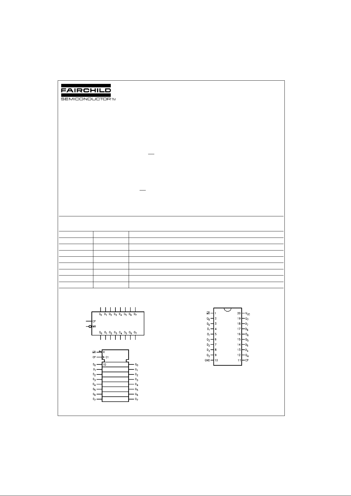
Logic Symbols
IEEE/IEC
Connection Diagram
FACT is a trademark of Fairchild Semiconductor Corporation.
Order Number Package Number Package Description
74AC273SC M20B 20-Lead Small Outline Integrated Circuit (SOIC), JEDEC MS-013, 0.300 Wide
74AC273SJ M20D 20-Lead Small Outline Package (SOP), EIAJ TYPE II, 5.3mm Wide
74AC273MTC MTC20 20-Lead Thin Shrink Small Outline Package (TSSOP), JEDEC MO-153, 4.4mm Wide
74AC273PC N20A 20-Lead Plastic Dual-In-Line Package (PDIP), JEDEC MS-001, 0.300 Wide
74ACT273SC M20B 20-Lead Small Outline Integrated Circuit (SOIC), JEDEC MS-013, 0.300 Wide
74ACT273SJ M20D 20-Lead Small Outline Package (SOP), EIAJ TYPE II, 5.3mm Wide
74ACT273MTC MTC20 20-Lead Thin Shrink Small Outline Package (TSSOP), JEDEC MO-153, 4.4mm Wide
74ACT273PC N20A 20-Lead Plastic Dual-In-Line Package (PDIP), JEDEC MS-001, 0.300 Wide
Page 2
www.fairchildsemi.com 2
74AC273 • 74ACT273
Pin Descriptions Mode Select-Function Table
H = HIGH Voltage Level
L = LOW Voltage Level
X = Immaterial
= LOW-to-HIGH Transition
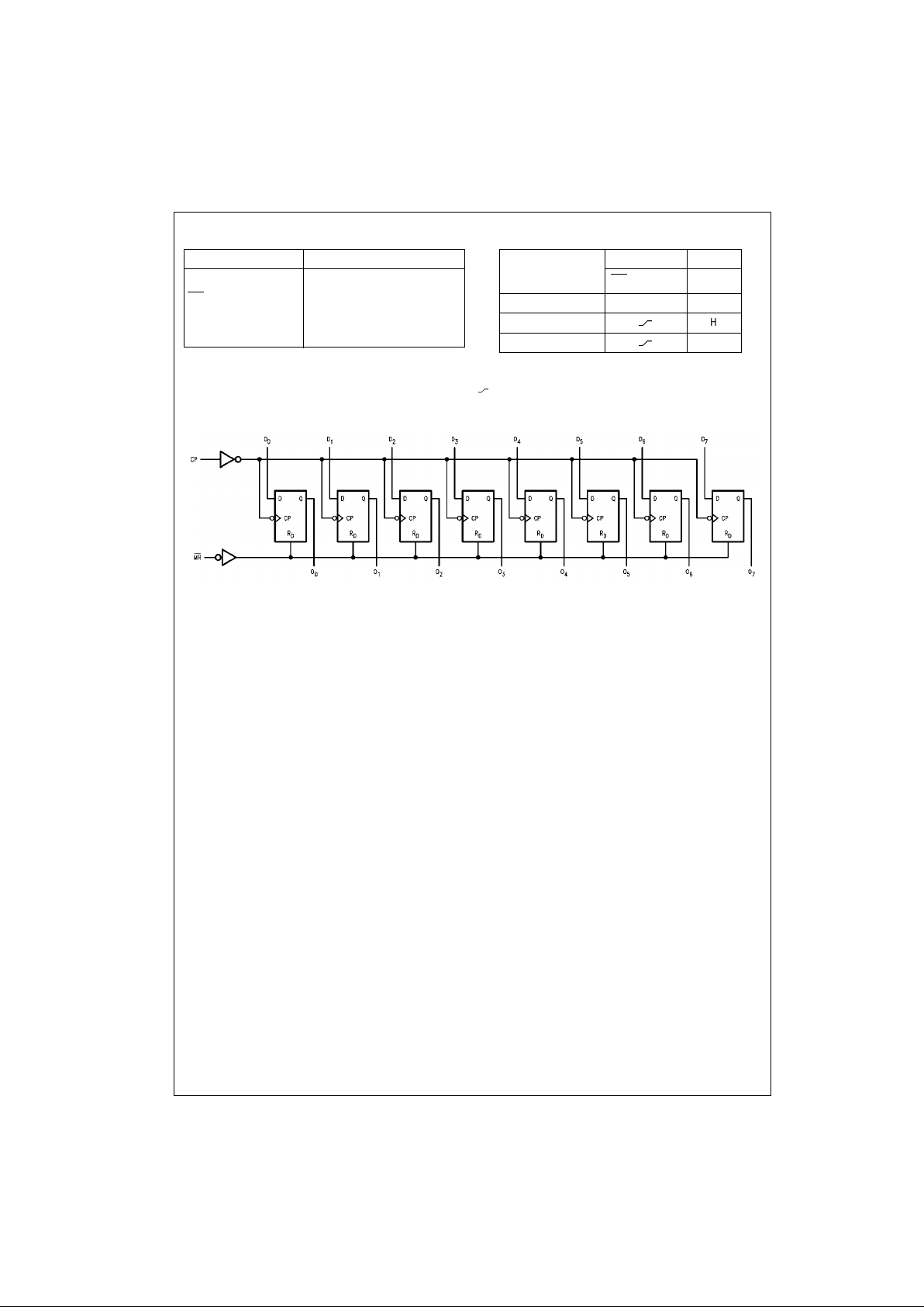
Logic Diagram
Please note that this diagram is provided only for the understanding of logic operations and should not be used to estimate propagation delays.
Pin Names Description
D
0–D7
Data Inputs
MR
Master Reset
CP Clock Pulse Input
Q
0–Q7
Data Outputs
Operating Mode
Inputs Outputs
MR
CP D
n
Q
n
Reset (Clear) L X X L
Load ‘1' H
HH
Load ‘0' H
LL
Page 3
3 www.fairchildsemi.com
74AC273 • 74ACT273
Absolute Maximum Ratings(Note 1) Recommended Operating
Conditions
Note 1: Absolute max imum ratings are those values beyond w hich damage
to the device may occu r. The databook spe cificatio ns shou ld be met, wit hout exception, to ensure that the system de sign is relia ble over its p ower
supply, temperature, and output/input loading variables. Fairchild does not
recommend operation of FACT circuits outside databook specif ic at ions.
DC Electrical Characteristics for AC
Note 2: All outputs loaded; thres holds on input associate d w it h output under test.
Note 3: Maximum test duration 2.0 ms, one output loaded at a time.
Note 4: I
IN
and ICC @ 3.0V are guaranteed to be less than or equa l t o th e respective limit @ 5.5V VCC.
Supply Voltage (VCC) −0.5V to +7.0V
DC Input Diode Current (I
IK
)
V
I
= −0.5V −20 mA
V
I
= VCC + 0.5V +20 mA
DC Input Voltage (V
I
) −0.5V to VCC + 0.5V
DC Output Diode Current (I
OK
)
V
O
= −0.5V −20 mA
V
O
= VCC + 0.5V +20 mA
DC Output Voltage (V
O
) −0.5V to VCC + 0.5V
DC Output Source
or Sink Current (I
O
) ± 50 mA
DC V
CC
or Ground Current
per Output Pin (I
CC
or I
GND
) ± 50 mA
Storage Temperature (T
STG
) −65°C to +150°C
Junction Temperature (T
J
)
(PDIP) 140
°C
Supply Voltage (V
CC
)
AC 2.0V to 6.0V
ACT 4.5V to 5.5V
Input Voltage (V
I
)0V to V
CC
Output Voltage (VO)0V to V
CC
Operating Temperature (TA) −40°C to +85°C
Minimum Input Edge Rate (
∆V/∆t)
AC Devices
V
IN
from 30% to 70% of V
CC
VCC @ 3.3V, 4.5V, 5.5V for AC 125 mV/ns
Minimum Input Edge Rate (
∆V/∆t)
ACT Devices
V
IN
from 0.8V to 2.0V
V
CC
@ 4.5V, 5.5V for ACT 125 mV/ns
Symbol Parameter
V
CC
TA = +25°CT
A
= −40°C to +85°C
Units Conditions
(V) Typ Guaranteed Limits
V
IH
Minimum HIGH Level 3.0 1.5 2.1 2.1 V
OUT
= 0.1V
Input Voltage 4.5 2.25 3.15 3.15 V or VCC − 0.1V
5.5 2.75 3.85 3.85
V
IL
Maximum LOW Level 3.0 1.5 0.9 0.9 V
OUT
= 0.1V
Input Voltage 4.5 2.25 1.35 1.35 V or VCC − 0.1V
5.5 2.75 1.65 1.65
V
OH
Minimum HIGH Level 3.0 2.99 2.9 2.9
Output Voltage 4.5 4.49 4.4 4.4 V I
OUT
= −50 µA
5.5 5.49 5.4 5.4
VIN = VIL or V
IH
3.0 2.56 2.46 IOH = −12 mA
4.5 3.86 3.76 V I
OH
= −24 mA
5.5 4.86 4.76 I
OH
= −24 mA (Note 2)
V
OL
Maximum LOW Level 3.0 0.002 0.1 0.1
Output Voltage 4.5 0.001 0.1 0.1 V I
OUT
= 50 µA
5.5 0.001 0.1 0.1
VIN = VIL or V
IH
3.0 0.36 0.44 IOL = 12 mA
4.5 0.36 0.44 V IOL = 24 mA
5.5 0.36 0.44 IOL = 24 mA (Note 2)
I
IN
Maximum Input
5.5 ±0.1 ±1.0 µAVI = VCC, GND
(Note 4) Leakage Current
I
OLD
Minimum Dynamic 5.5 75 mA V
OLD
= 1.65V Max
I
OHD
Output Current (Note 3) 5.5 −75 mA V
OHD
= 3.85V Min
I
CC
Maximum Quiescent
5.5 4.0 40.0 µA
VIN = V
CC
(Note 4) Supply Current or GND
Page 4

www.fairchildsemi.com 4
74AC273 • 74ACT273
AC Electrical Characteristics for AC
Note 5: Voltage Range 3.3 is 3.3V ± 0.3V
Voltage Range 5.0 is 5.0V ± 0.5V
AC Operating Requirements for AC
Note 6: Voltage Range 3.3 is 3.3V ± 0.3V
Voltage Range 5.0 is 5.0V ± 0.5V
V
CC
TA = +25°CT
A
= −40°C to +85°C
Symbol Parameter (V)
C
L
= 50 pF CL = 50 pF
Units
(Note 5) Min Typ Max Min Max
f
MAX
Maximum Clock 3.3 90 125 75
MHz
Frequency 5.0 140 175 125
t
PLH
Propagation Delay 3.3 4.0 7.0 12.5 3.0 14.0
ns
Clock to Output 5.0 3.0 5.5 9.0 2.5 10.0
t
PHL
Propagation Delay 3.3 4.0 7.0 13.0 3.5 14.5
ns
Clock to Output 5.0 3.0 5.0 10.0 2.5 11.0
t
PHL
Propagation Delay 3.3 4.0 7.0 13.0 3.5 14.0
ns
MR
to Output 5.0 3.0 5.0 10.0 2.5 10.5
V
CC
TA = +25°CT
A
= −40°C to +85°C
Symbol Parameter (V)
C
L
= 50 pF CL = 50 pF
Units
(Note 6) Typ Guaranteed Minimum
t
S
Setup Time, HIGH or LOW 3.3 3.5 5.5 6.0
ns
Data to CP 5.0 2.5 4.0 4.5
t
H
Hold Time, HIGH or LOW 3.3 −2.0 0 0
ns
Data to CP 5.0 −1.0 1.0 1.0
t
W
Clock Pulse Width 3.3 3.5 5.5 6.0
ns
HIGH or LOW 5.0 2.5 4.0 4.5
t
W
MR Pulse Width 3.3 2.0 5.5 6.0
ns
HIGH or LOW 5.0 1.5 4.0 4.5
t
rec
Recovery Time 3.3 1.5 3.5 4.5
ns
MR to CP 5.0 1.0 2.0 3.0
Page 5

5 www.fairchildsemi.com
74AC273 • 74ACT273
DC Electrical Characteristics for ACT
Note 7: All outputs loaded; thres holds on input associate d w it h output under test.
Note 8: Maximum test duration 2.0 ms, one output loaded at a time.
AC Electrical Characteristics for ACT
Note 9: Voltage Range 5.0 is 5.0V ± 0.5V
Symbol Parameter
V
CC
TA = +25°CT
A
= −40°C to +85°C
Units Conditions
(V) Typ Guaranteed Limits
V
IH
Minimum HIGH Level 4.5 1.5 2.0 2.0
V
V
OUT
= 0.1V
Input Voltage 5.5 1.5 2.0 2.0 or VCC − 0.1V
V
IL
Maximum LOW Level 4.5 1.5 0.8 0.8
V
V
OUT
= 0.1V
Input Voltage 5.5 1.5 0.8 0.8 or V
CC
− 0.1V
V
OH
Minimum HIGH Level 4.5 4.49 4.4 4.4
VI
OUT
= −50 µA
Output Voltage 5.5 5.49 5.4 5.4
VIN = VIL or V
IH
4.5 3.86 3.76 V IOH = −24 mA
5.5 4.86 4.76 I
OH
= −24 mA (Note 7)
V
OL
Maximum LOW Level 4.5 0.001 0.1 0.1
VI
OUT
= 50 µA
Output Voltage 5.5 0.001 0.1 0.1
VIN = VIL or V
IH
4.5 0.36 0.44 V IOL = 24 mA
5.5 0.36 0.44 IOL = 24 mA (Note 7)
I
IN
Maximum Input
5.5 ±0.1 ±1.0 µAVI = VCC, GND
Leakage Current
I
CCT
Maximum
5.5 0.6 1.5 mA VI = V
CC
− 2.1V
ICC/Input
I
OLD
Minimum Dynamic 5.5 75 mA V
OLD
= 1.65V Max
I
OHD
Output Current (Note 8) 5.5 −75 mA V
OHD
= 3.85V Min
I
CC
Maximum Quiescent
5.5 4.0 40.0 µA
VIN = V
CC
Supply Current or GND
V
CC
TA = +25°CT
A
= −40°C to +85°C
Symbol Parameter (V)
C
L
= 50 pF CL = 50 pF
Units
(Note 9) Min Typ Max Min Max
f
MAX
Maximum Clock Frequency 2.0 125 189 110 MHz
t
PLH
Propagation Delay
5.0 1.5 6.5 8.5 1.5 9.0 ns
t
PHL
CP to Q
n
t
PHL
Propagation Delay
5.0 1.5 7.0 9.0 1.5 8.5 ns
MR to Q
n
Page 6

www.fairchildsemi.com 6
74AC273 • 74ACT273
AC Operating Requirements for ACT
Note 10: Voltage Range 5.0 is 5.0V ± 0.5V
Capacitance
V
CC
TA = +25°CT
A
= −40°C to +85°C
Symbol Parameter (V)
CL = 50 pF CL = 50 pF
Units
(Note 10) Typ Guaranteed Minimum
t
S
Setup Time, HIGH or LOW
5.0 1.0 3.5 3.5 ns
Dn to CP
t
H
Hold Time, HIGH or LOW
5.0 −0.5 1.5 1.5 ns
Dn to CP
t
W
Clock Pulse Width
5.0 2.0 4.0 4.0 ns
HIGH or LOW
t
W
MR Pulse Width
5.0 1.5 4.0 4.0 ns
HIGH or LOW
t
W
Recovery Time
5.0 0.5 3.0 3.0 ns
MR to CP
Symbol Parameter Typ Units Conditions
C
IN
Input Capacitance 4.5 pF VCC = OPEN
C
PD
Power Dissipation Capacitance for AC 50.0
pF V
CC
= 5.0V
Power Dissipation Capacitance for ACT 40.0
Page 7

7 www.fairchildsemi.com
74AC273 • 74ACT273
Physical Dimensions inches (millimeters) unless otherwise noted
20-Lead Small Outline Integrated Circuit (SOIC), JEDEC MS-013, 0.300 Wide
Package Number M20B
Page 8

www.fairchildsemi.com 8
74AC273 • 74ACT273
Physical Dimensions inches (millimeters) unless otherwise noted (Continued)
20-Lead Small Outline Package (SOP), EIAJ TYPE II, 5.3mm Wide
Package Number M20D
Page 9

9 www.fairchildsemi.com
74AC273 • 74ACT273
Physical Dimensions inches (millimeters) unless otherwise noted (Continued)
20-Lead Thin Shrink Sm all Ou tline Pa ck age (TS SO P), JE DE C MO-153, 4.4mm Wide
Package Number MTC20
Page 10

www.fairchildsemi.com 10
74AC273 • 74ACT273 Octal D-Type Flip-Flop
Physical Dimensions inches (millimeters) unless otherwise noted (Continued)
20-Lead Plastic Dual-In-Line Package (PDIP), JEDEC MS-001, 0.300 Wide
Package Number N20A
Fairchild does not assume any responsibility for use of any circuitr y described, no circuit patent licenses are implied and
Fairchild reserves the right at any time without notice to change said circuitry and specifications.
LIFE SUPPORT POLICY
FAIRCHILD’S PRODUCTS ARE NOT AUTHORIZED FOR USE AS CRITICAL COMPONENTS IN LIFE SUPPORT
DEVICES OR SYSTEMS WITHOUT THE EXPRESS WRITTEN APPROVAL OF THE PRESIDENT OF FAIRCHILD
SEMICONDUCTOR CORPORATION. As used herein:
1. Life support devices or systems are devices or syste ms
which, (a) are intended for surgical implant into the
body, or (b) support or sustain life, and (c) whose failure
to perform when properly used in accordance with
instructions for use provided in the labeling, can be reasonably expected to result in a significant inju ry to the
user.
2. A critical component in any compon ent of a lif e supp ort
device or system whose failure t o perform can be reasonably expected to ca use the failure of the life supp ort
device or system, or to affect its safety or effectiveness.
www.fairchildsemi.com
 Loading...