

Page 1
WITH 3-STATE OUTPUTS (NON INVERTED)
■ HIGH SPEED:
t
= 4.5 ns (TYP.) at VCC=5V
PD
■ LOW POWER DISSIPATION:
I
=8µA (MAX.) at TA=25°C
CC
■ HIGH NOISE IMMUNITY:
V
NIH=VNIL
■ POWER DOWN PROTECTION ON INPUTS
■ SYMMETRICAL OUTPUT IMPEDANCE:
|I
|=IOL=24mA(MIN)
OH
■ BALANCED PROPAGATION DELAYS:
t
≅ t
PLH
■ OPERATING VOLTAGE RANGE:
V
(OPR) = 2V to 6V
CC
■ PIN AND FUNCTION COMPATIBLE WITH
74 SERIES 16541
■ IMPROVED LATCH-UP IMMUNITY
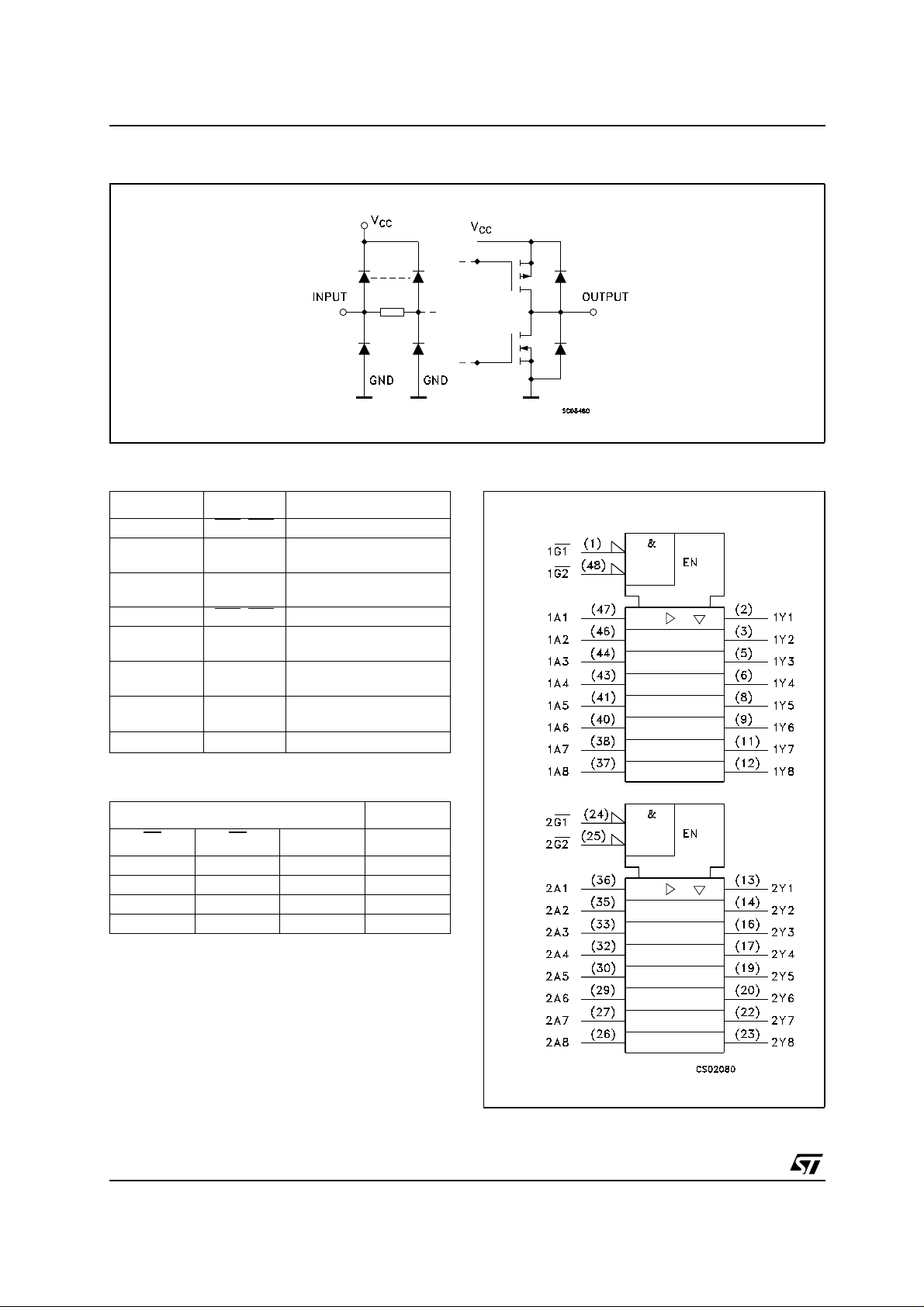
DESCRIPTION
The 74AC16541 is an advanced high-speed
CMOS 16-BIT BUS BUFFER (3-STATE) fabricated with sub-micron silicon gate and double-layer
metal wiring C
This is composed of two 8-bit sections with
separate output-enable signals. For either 8-bit
buffers section, the 3 STATE control gate
operates as a two input AND such that if either
nG1
and nG2 are high, all outputs are in the high
impedence state.
= 28% VCC(MIN.)
PHL
2
MOS tecnology.
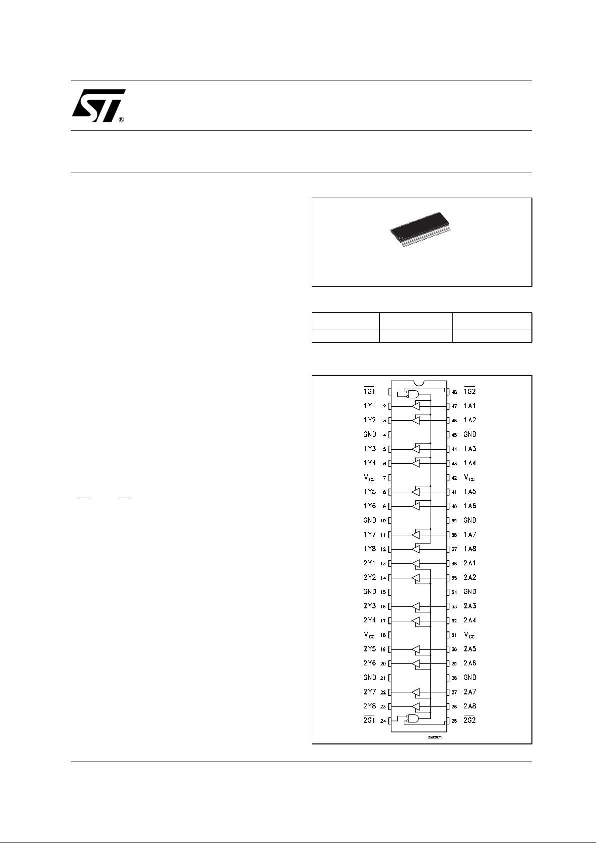
74AC16541
16-BIT BUS BUFFER
TSSOP
ORDER CODES
PACKAGE TUBE T & R
TSSOP 74AC16541TTR
PIN CO NNECTION
1/9February 2003
Page 2
74AC16541
INPUT AND OUTP UT EQUIVALENT CIRCUIT
PIN DESCRIPTION
PIN No SYMBOL NAME AND FUNCTION
1, 48 1G1
2, 3,5,6,8, 9,
11, 12
13,14,16, 17,
19, 20, 22, 23
24, 25 2G1
36,35,33, 32,
30, 29, 27, 26
47,46,44, 43,
41, 40, 38, 37
4, 10, 15, 21,
28, 34, 39, 45
7, 18, 31, 42 V
,1G2 Output Enable Inputs
1Y1 to 1Y8 Data Outputs
2Y1 to 2Y8 Data Outputs
,2G2 Output Enable Inputs
2A1 to 2A8 Data Outputs
1A1 to 1A8 Data Outputs
GND Ground (0V)
CC
Positive Supply Voltage
TRUTH TABLE
INPUTS OUTPUT
G1
HXXZ
XHXZ
LLHH
LLLL
X : Don’t Care
Z : High Impedance
G2 An Yn
IEC LOGIC SYMBOLS
2/9
Page 3
74AC16541
ABSOLUTE MAXIMUM RATINGS
Symbol Parameter Value Unit
V
V
V
I
I
OK
I
or I
I
CC
T
stg
T
Absolute Maximum Ratings are those values beyond which damage to the device may occur. Functional operation under these conditions is
not implied
RECOMMENDED OPERATING CONDITIONS
Symbol Parameter Value Unit
V
V
V
T
dt/dv Input Rise and Fall Time (note 1) V
1) VINfrom30% to 70%of V
Supply Voltage
CC
DC Input Voltage
I
DC Output Voltage -0.5 to VCC+ 0.5
O
DC Input Diode Current
IK
DC Output Diode Current
DC Output Current
O
DC VCCor Ground Current
GND
Storage Temperature
Lead Temperature (10 sec)
L
Supply Voltage
CC
Input Voltage 0 to V
I
Output Voltage 0 to V
O
Operating Temperature
op
= 3.0, 4.5 or 5.5
CC
CC
-0.5 to +7.0 V
-0.5 to +7.0 V
± 20 mA
± 50 mA
± 50 mA
± 400 mA
-65 to +150 °C
300 °C
2to6 V
CC
CC
-55 to 125 °C
0to8
ns/V
V
V
V
3/9
Page 4

74AC16541
DC SPECIFICATIONS
Symbol Parameter
V
V
V
I
High Level Input
IH
Voltage
V
Low Level Input
IL
Voltage
High Level Output
OH
Voltage
Low Level Output
OL
Voltage
Input Leakage
I
I
Current
High Impedance
I
OZ
Output Leakage
Current
Quiescent Supply
CC
Current
Test Condition Value
=25°C
T
V
CC
(V)
3.0
5.5 3.85 2.75 3.85 3.85
3.0
5.5 2.75 1.65 1.65 1.65
3.0
4.5
5.5
3.0
4.5
5.5
3.0
4.5
5.5
3.0
4.5
5.5
5.5
5.5
V
= 0.1 V or
O
V
-0.1V
CC
= 0.1 V or
V
O
V
-0.1V
CC
IO=-50 µA
=-50 µA
I
O
=-50 µA
I
O
=-12 mA
I
O
=-24 mA
I
O
=-24 mA
I
O
IO=50 µA
=50 µA
I
O
=50 µA
I
O
=12 mA
I
O
I
=24 mA
O
I=VIH
or GND
or V
IL
V
I=VCC
V
VO=VCCor GND
V
I=VCC
or GND
A
Min. Typ. Max. Min. Max. Min. Max.
2.1 1.5 2.1 2.1
1.5 0.9 0.9 0.9
2.9 2.99 2.9 2.9
4.4 4.49 4.4 4.4
5.4 5.49 5.4 5.4
2.56 2.46 2.46
3.86 3.76 3.76
4.86 4.76 4.76
0.002 0.1 0.1 0.1
0.001 0.1 0.1 0.1
0.001 0.1 0.1 0.1
-40 to 85°C -55 to 125°C
0.36 0.44 0.44
0.36 0.44 0.44
± 0.1 ± 1 ± 1 µA
± 0.5 ± 5 ± 5 µA
88080µA
Unit
V4.5 3.15 2.25 3.15 3.15
V4.5 2.25 1.35 1.35 1.35
V
V
AC ELECTRICAL C HARACTERISTICS (C
Test Condition Value
Symbol Parameter
t
PLHtPHL
Propagation Delay
Time
AtoY
t
PZLtPZH
t
PLZtPHZ
(*) Voltagerange is3.3V ± 0.3V
(**) Voltage range is 5.0V ± 0.5V
Output Enable
Time
Output Disable
Time
4/9
3.3
5.0
3.3
5.0
3.3
5.0
V
(V)
CC
(*)
(**)
(*)
(**)
(*)
(**)
C
(pF)
L
=50pF,RL= 500 Ω, Input tr=tf= 3ns)
L
= 25°C
T
A
-40 to 85°C -55 to 125°C
Min. Typ. Max. Min. Max. Min. Max.
6.3 7.5 9.5 9.5
4.5 7.0 9.0 9.0
8.5 10.0 12.0 12.0
5.5 7.0 9.0 9.0
7.5 9.0 11.5 11.5
6.0 8.0 11.0 11.0
Unit
ns
ns
ns
Page 5

74AC16541
CAPACITIVE CHARACTERISTICS
Test Condition Value
= 25°C
Symbol Parameter
C
C
C
Input Capacitance
IN
Output
OUT
Capacitance
Power Dissipation
PD
Capacitance
V
(V)
5.0
CC
= 10MHz
f
IN
T
A
Min. Typ. Max. Min. Max. Min. Max.
710 10 10pF
14 pF
25 pF
(note 1)
1) CPDis defined as the value of the IC’s internal equivalent capacitance which is calculated from the operating current consumption without
load. (Refer to Test Circuit). Average operating current can be obtained by the following equation. I
TEST CIRCUIT
-40 to 85°C -55 to 125°C
CC(opr)=CPDxVCCxfIN+ICC
Unit
/16
TEST SWITCH
t
PLH,tPHL
t
PZL,tPLZ
t
PZH,tPHZ
CL= 50 pF or equivalent (includes jig and probe capacitance)
=R1=500Ω or equivalent
R
L
R
T=ZOUT
of pulse generator (typically 50Ω)
Open
V
CC
GND
5/9
Page 6

74AC16541
WAVEFORM 1: PROPAG ATION DELAYS (f=1MHz; 50% duty cycle)
WAVEFORM 2: OUTPUT ENABLE AND D ISABLE TIME (f=1MHz; 50% duty cycle)
6/9
Page 7

74AC16541
TSSOP48 MECHANICAL DATA
mm. inch
DIM.
MIN. TYP MAX. MIN. TYP. MAX.
A 1.2 0.047
A1 0.05 0.15 0.002 0.006
A2 0.9 0.035
b 0.17 0.27 0.0067 0.011
c 0.09 0.20 0.0035 0.0079
D 12.4 12.6 0.488 0.496
E 8.1 BSC 0.318 BSC
E1 6.0 6.2 0.236 0.244
e 0 .5 BSC 0.0197 BSC
K0˚ 8˚0˚ 8˚
L 0.50 0.75 0.020 0.030
A2
A
A1
b
e
D
K
c
E1
L
E
PIN 1 IDENTIFICATION
1
7065588C
7/9
Page 8

74AC16541
Tape & Reel TSSOP48 MECHANICAL DATA
mm. inch
DIM.
MIN. TYP MAX. MIN. TYP. MAX.
A 330 12.992
C 12.8 13.2 0.504 0.519
D 20.2 0.795
N 60 2.362
T 30.4 1.197
Ao 8.7 8.9 0.343 0.350
Bo 13.1 13.3 0.516 0.524
Ko 1.5 1.7 0.059 0.067
Po 3.9 4.1 0.153 0.161
P 11.9 12.1 0.468 0.476
8/9
Page 9

74AC16541
Information furnished is believed to be accurate and reliable. However, STMicroelectronics assumes no responsibility for the
consequences of use o f suc h inf ormat ion n or f or an y infr ingeme nt of paten ts or oth er ri gh ts of third part ies whic h may resul t f rom
its use. No license is granted by implication or otherwise under any patent or patent rights of STMicroelectronics. Specifications
mentioned in this publication are subject to change without notice. This publication supersedes and replaces all information
previously supplied. STMicroelectronics products are not authorized for use as critical components in life support devices or
systems without express written approval of STMicroelectronics.
Australia - Brazil - Canada - China - Finland - France - Germany - Hong Kong - India - Israel - Italy - Japan - Malaysia - Malta - Morocco
© The ST logo is a registered trademark of STMicroelectronics
© 2003 STMicroelectronics - Printed in Italy - All Rights Reserved
STMicroelectronics GROUP OF COMPANIES
Singapore - Spain - Sweden - Switzerland - United Kingdom - United States.
© http://www.st.com
9/9
 Loading...