

Page 1
QUAD 2 CHANNEL MULTIPLEXER
■ HIGH SPEED:t
■ LOWPOWER DISSIPATION:
=8µA (MAX.)at TA=25oC
I
CC
■ HIGH NOISE IMMUNITY:
V
NIH=VNIL
■ 50Ω TRANSMISSION LINE DRIVING
CAPABILITY
■ SYMMETRICAL OUTPUT IMPEDANCE:
|I
|=IOL=24mA (MIN)
OH
■ BALANCE DPROPAGATIONDELAYS:
t
≅ t
PLH
PHL
■ OPERATINGVOLTAGERANGE:
V
(OPR) = 2V to 6V
CC
■ PIN AND FUNCTION COMPATIBLE WITH
74SERIES 157
■ IMPROVED LATCH-UP IMMUNITY
DESCRIPTION
The AC157 is an high-speed CMOS QUAD
2-CHANNEL MULTIPLEXER fabricated with
sub-micron silicon gate and double-layer metal
wiring C
2
MOS technology. It is ideal for low
power applications maintaining high speed
operation similar to equivalent Bipolar Schottky
TTL.
=4 ns(TYP.)atVCC=5V
PD
=28%VCC(MIN.)
74AC157
PRELIMINARY DATA
B
(Plastic Package)
(Micro Package)
ORDERCODES:
74AC157B 74AC157M
It consists of four 2-input digital multiplexers with
common select and strobe inputs. It is a
non-inverting multiplexer. When the STROBE
input is held high selection of data is inhibit and
all the outputs become low. The SELECT
decoding determines whether the A or B inputs
get routed to their correspondingY outputs.
All inputs and outputs are equipped with
protectioncircuits against static discharge, giving
them 2KV ESD immunity and transient excess
voltage.
M
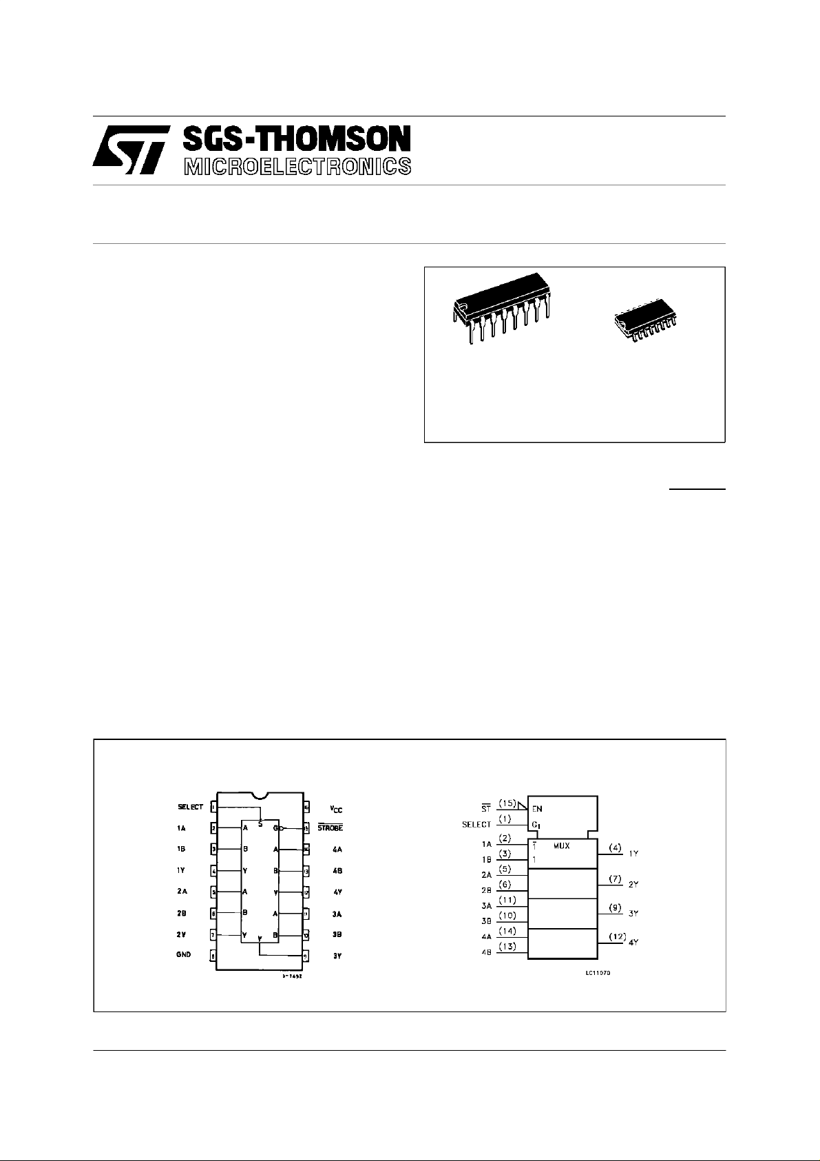
PINCONNECTION ANDIEC LOGICSYMBOLS
May 1997
1/9
Page 2
74AC157
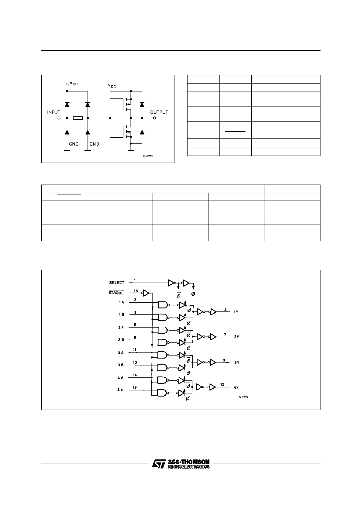
INPUTAND OUTPUT EQUIVALENTCIRCUIT
PIN DESCRIPTION
PI N No SYM B O L NAME A ND FUNCTI ON
1 SELECT Common Data Select Input
2,5, 11, 14 1Ato4A Data Inputs From
Source A
3,6, 10, 13 1Bto4B Data Inputs From
Source B
4,7, 9,12 1Yto4Y Multiplexer Outputs
15 STROBE Strobe Input
8 GND Ground (0V)
16 V
CC
Positive Supply Voltage
TRUTH TABLE
INPUT OUTPUT
ST RO B E SE L ECT A B Y
HXXXL
LLLXL
LLHXH
LHXLL
LHXHH
X:”H”or”L”
LOGICDIAGRAM
2/9
Page 3
74AC157
ABSOLUTE MAXIMUMRATING
Symb o l Parame t er Value Unit
V
V
V
I
I
OK
I
orI
I
CC
T
T
Absolute Maximum Ratings are those values beyond which damage to the device may occur. Functional operation under these condition is not implied.
RECOMMENDED OPERATINGCONDITIONS
Symb o l Parame t er Val u e Uni t
V
V
V
T
dt/dv Input Rise and Fall Time V
1) VINfrom30% to70%of V
Supply Voltage -0.5to+7 V
CC
DC Input Voltage -0.5toVCC+0.5 V
I
DC Output Voltage -0.5toVCC+0.5 V
O
DC Input Diode Current ± 20 mA
IK
DC Output Diode Current ± 20 mA
DC Output Current ± 50 mA
O
DC VCCor Ground Current ± 200 mA
GND
Storage Temperature -65to+150
stg
Lead Temperature (10 sec) 300
L
Supply Voltage 2to6 V
CC
Input Voltage 0toV
I
Output Voltage 0toV
O
Operating Temperature: -40to+85
op
= 3.0, 4.5 or 5.5 V(note 1) 8 ns/V
CC
CC
CC
CC
o
C
o
C
V
V
o
C
3/9
Page 4

74AC157
DC SPECIFICATIONS
Symbol Parameter Test Condition s Value Unit
V
CC
(V)
High Level Input Voltage 3.0 VO=0.1 Vor
V
IH
4.5 3.15 2.25 3.15
=25oC-40to85
T
A
Min. Ty p. Max. Min. Max.
2.1 1.5 2.1
V
-0.1 V
CC
o
C
5.5 3.85 2.75 3.85
Low Level Input Voltage 3.0 VO=0.1 Vor
V
IL
4.5 2.25 1.35 1.35
-0.1 V
V
CC
1.5 0.9 0.9
5.5 2.75 1.65 1.65
High Level Output
V
OH
Voltage
Low Level Output
V
OL
Voltage
Input Leakage Current
I
I
Quiescent Supply
I
CC
3.0
4.5 I
5.5 I
3.0 I
V
I
V
IH
V
4.5 I
5.5 I
3.0
4.5 I
5.5 I
3.0 I
V
I
V
IH
V
4.5 I
5.5 I
5.5
IO=-50µA 2.9 2.99 2.9
(*)
or
IL
=-50µA 4.4 4.49 4.4
O
=
=-50µA 5.4 5.49 5.4
O
=-12 mA 2.56 2.46
O
=-24 mA 3.86 3.76
O
=-24 mA 4.86 4.76
O
IO=50µA0.0020.1 0.1
(*)
=
or
IL
=50µA0.0010.1 0.1
O
=50µA0.0010.1 0.1
O
=12mA 0.36 0.44
O
=24mA 0.36 0.44
O
=24mA 0.36 0.44
O
VI=VCCorGND ±0.1 ±1 µA
5.5 VI=VCCorGND 8 80 µA
Current
Dynamic Output Current
I
OLD
(note 1, 2)
I
OHD
1) Maximum test duration 2ms, one output loaded at time
2) Incident wave switching is guaranteed on transmission lines with impedances as low as 50 Ω.
5.5 V
=1.65 Vmax 75 mA
OLD
V
=3.85Vmin -75 mA
OHD
V
V
V
V
4/9
Page 5

AC ELECTRICAL CHARACTERISTICS (CL= 50 pF, RL=500 Ω, Inputtr=tf=3ns)
74AC157
Symbol Parameter Test Cond iti on Value Unit
o
C
ns
ns
ns
t
Propagation Delay Time
PLH
t
SELECT to Y
PHL
Propagation Delay Time
t
PLH
STROBE to Y
t
PHL
Propagation Delay Time
t
PLH
t
A, B to Y
PHL
(*) Voltagerange is3.3V± 0.3V
(**) Voltage range is5V± 0.5V
V
(V)
3.3
5.0
3.3
5.0
3.3
5.0
CC
=25oC-40to85
T
A
Min. Ty p. Max. Min. Max.
(*)
(**)
(*)
(**)
(*)
(**)
1.5 6.5 11.0 1.5 12.0
1.55.08.51.59.5
1.5 6.5 11.0 1.5 12.0
1.5 5.5 9.0 1.5 10.0
1.55.08.01.59.0
1.54.06.51.57.0
CAPACITIVE CHARACTERISTICS
Symbol Parameter Test Condition s Value Unit
T
V
CC
(V)
Input Capacitance 5.0 4 pF
C
IN
Power Dissipation
C
PD
5.0 TBD pF
=25oC-40to85
A
Min. Ty p. Max. Min. Max.
Capacitance (note 1)
1) CPDis defined as the value of the IC’s internal equivalent capacitance which is calculated from the operating current consumption without load. (Refer to
Test Circuit). Average operating current can be obtained by the following equation. I
(opr) = CPD• VCC• fIN+ICC/n (per circuit)
CC
o
C
TEST CIRCUIT
5/9
Page 6

74AC157
WAVEFORM 1: PROPAGATIONDELAYS FOR INVERTING CONDITIONS
WAVEFORM 2: PROPAGATIONDELAYS FOR NON-INVERTING CONDITIONS
6/9
Page 7

Plastic DIP-16 (0.25) MECHANICALDATA
74AC157
DIM.
MIN. TYP. MAX. MIN. TYP. MAX.
a1 0.51 0.020
B 0.77 1.65 0.030 0.065
b 0.5 0.020
b1 0.25 0.010
D 20 0.787
E 8.5 0.335
e 2.54 0.100
e3 17.78 0.700
F 7.1 0.280
I 5.1 0.201
L 3.3 0.130
Z 1.27 0.050
mm inch
P001C
7/9
Page 8

74AC157
SO-16 MECHANICAL DATA
DIM.
MIN. TYP. MAX. MIN. TYP. MAX.
A 1.75 0.068
a1 0.1 0.2 0.004 0.007
a2 1.65 0.064
b 0.35 0.46 0.013 0.018
b1 0.19 0.25 0.007 0.010
C 0.5 0.019
c1 45 (typ.)
D 9.8 10 0.385 0.393
E 5.8 6.2 0.228 0.244
e 1.27 0.050
e3 8.89 0.350
F 3.8 4.0 0.149 0.157
G 4.6 5.3 0.181 0.208
L 0.5 1.27 0.019 0.050
M 0.62 0.024
S 8 (max.)
mm inch
8/9
P013H
Page 9

74AC157
Information furnished is believedtobe accurateand reliable.However,SGS-THOMSON Microelectronics assumes no responsability for the
consequencesof use of such information nor for any infringement of patentsor other rights of third parties whichmay resultsfrom its use. No
licenseis grantedby implication or otherwise underany patent or patentrights of SGS-THOMSON Microelectronics. Specifications mentioned
in this publication are subject to change without notice. This publication supersedes andreplacesall informationpreviouslysupplied.
SGS-THOMSONMicroelectronics productsarenotauthorizedfor useascritical components inlifesupportdevices or systems withoutexpress
writtenapproval of SGS-THOMSON Microelectonics.
1997 SGS-THOMSONMicroelectronics - Printedin Italy - All Rights Reserved
Australia- Brazil - Canada - China- France- Germany- HongKong - Italy- Japan- Korea- Malaysia- Malta - Morocco- TheNetherlands-
Singapore- Spain- Sweden- Switzerland - Taiwan - Thailand - UnitedKingdom- U.S.A
SGS-THOMSONMicroelectronics GROUPOF COMPANIES
.
9/9
 Loading...