

Page 1
查询74AC153MTC供应商
74AC153 • 74ACT153
Dual 4-Input Multiplexer
74AC153 • 74ACT153 Dual 4-Input Multiplexer
November 1988
Revised November 1999
General Description
The AC/ACT153 is a hi gh-speed dual 4-input multiplex er
with common select inpu ts and in dividu al enab le inp uts for
each section. It can select two lines of data from four
sources. The two buffered outpu ts pre sent d ata i n t he tr ue
(non-inverted) form. In addition to multiplexer operation,
the AC/ACT153 can act as a function generator and generate any two functions of three variables.
Features
■ ICC reduced by 50%
■ Outputs source/sink 24 mA
■ ACT153 has TTL-compatible inputs
Ordering Code:
Order Number Package Number Package Description
74AC153SC M16A 16-Lead Small Outline Integrated Circuit (SOIC), JEDEC MS-012, 0.150” Narrow Body
74AC153SJ M16D 16-Lead Small Outline Package (SOP), EIAJ TYPE II, 5.3mm Wide
74AC153MTC MTC16 16-Lead Thin Shrink Small Outline Package (TSSOP), JEDEC MO-153, 4.4mm Wide
74AC153PC N16E 16-Lead Plastic Dual-In-Line Package (PDIP), JEDEC MS-001, 0.300” Wide
74ACT153SC M16A 16-Lead Small Outline Integrated Circuit (SOIC), JEDEC MS-012, 0.150” Narrow Body
74ACT153MTC MTC16 16-Lead Thin Shrink Small Outline Package (TSSOP), JEDEC MO-153, 4.4mm Wide
Device also available in Tape and Reel. Specify by appending suffix letter “X” to the or dering code.
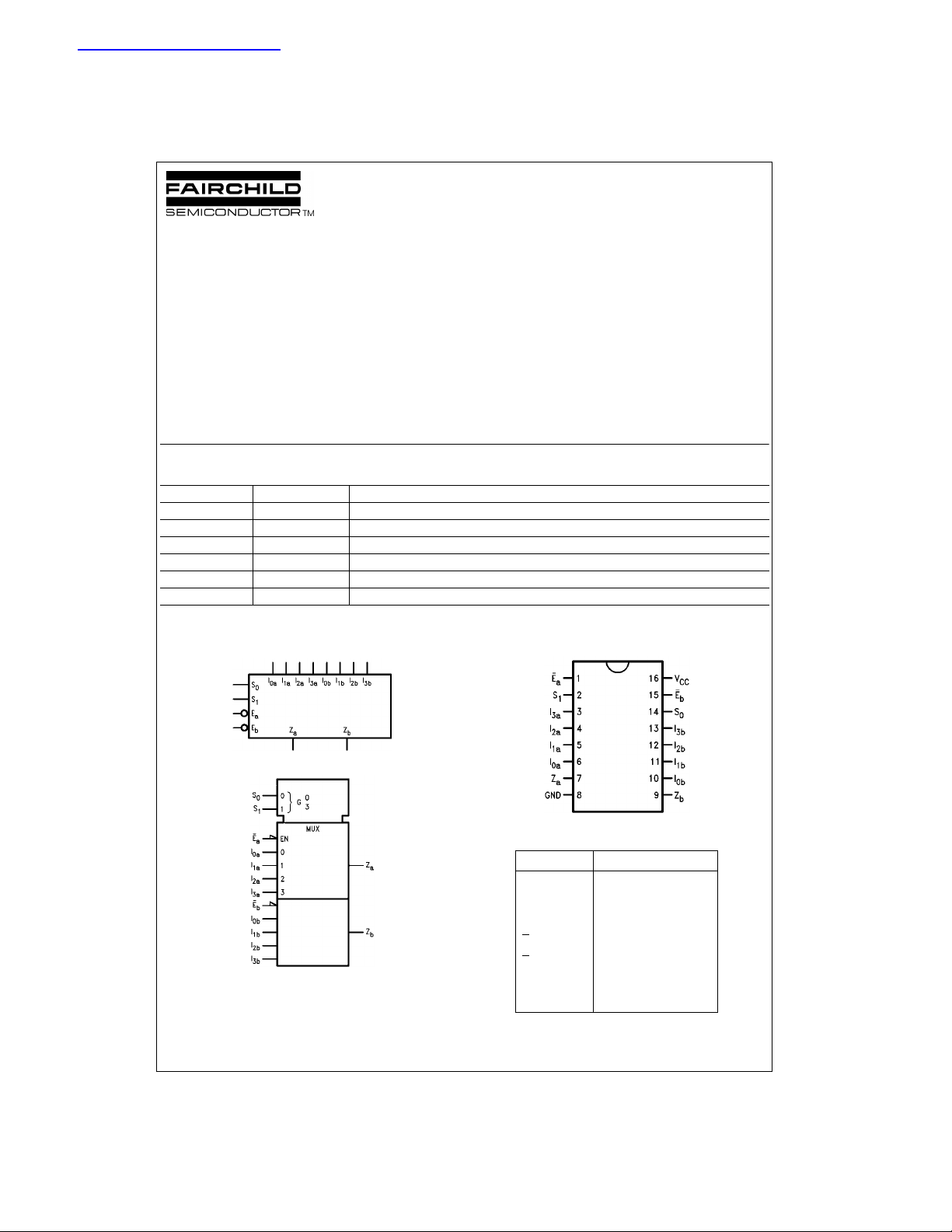
Logic Symbols
IEEE/IEC
Connection Diagram
Pin Descriptions
Pin Names Description
I
0a–I3a
I
0b–I3b
S
, S
0
1
E
a
E
b
Z
a
Z
b
FACT is a trademark of Fairchild Semiconductor Corporation.
© 1999 Fairchild Semiconductor Corporation DS009928 www.fairchildsemi.com
Side A Data Inputs
Side B Data Inputs
Common Select Inputs
Side A Enable Input
Side B Enable Input
Side A Output
Side B Output
Page 2
Functional Description
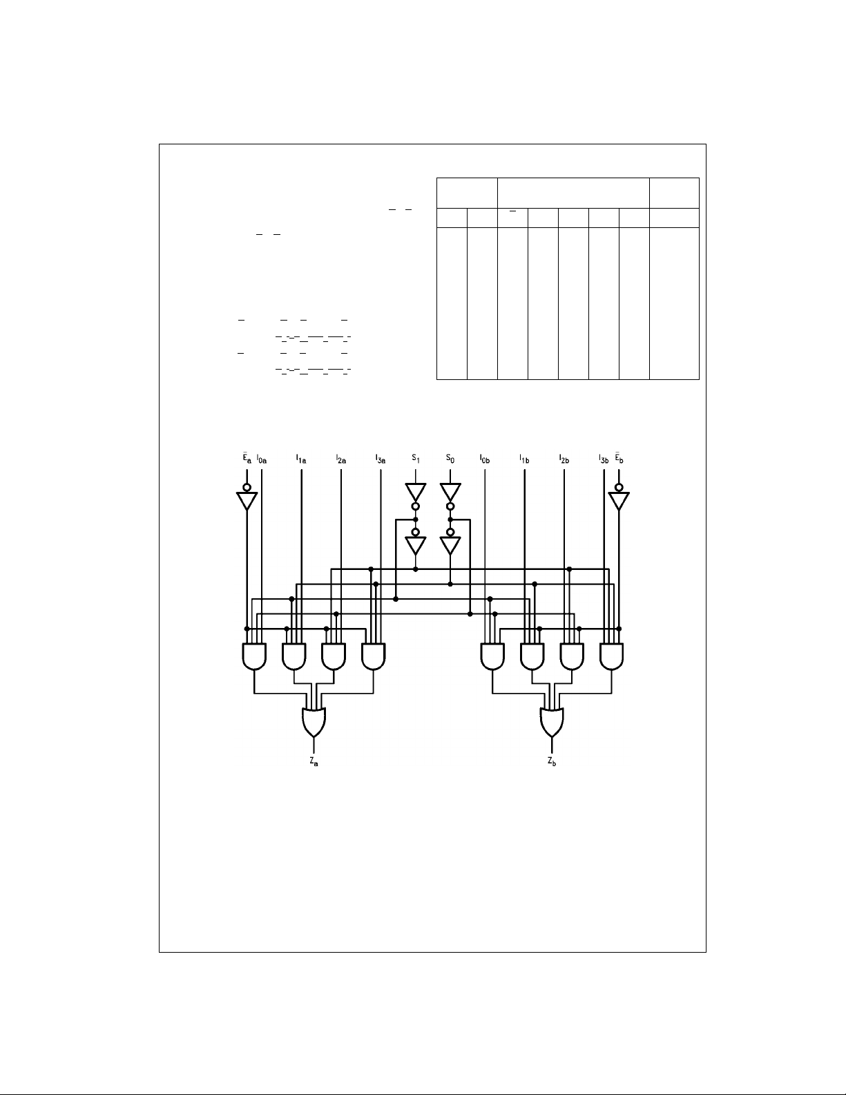
The AC/ACT153 is a dua l 4-input multiplexer. It can select
two bits of data from up to four sources under the control of
the common Select inputs (S
, S1). The two 4-input multi-
0
plexer circ ui ts ha v e in di vi d ua l ac t iv e- L OW En ab les ( E
which can be used to strobe the outputs independently.
When the Enables ( E
outputs Z
, Zb) are forced LOW. The AC/ACT153 is the
a
, Eb) are HIGH, the corre sponding
a
logic implementatio n of a 2-pole, 4-positi on switch, where
the position of the sw itch is determined b y the logic level s
supplied to the Select i nputs. The logic equations f or the
74AC153 • 74ACT153
outputs are shown below.
Z
= Ea • (I0a • S1 • S0 + I1a • S1 • S0 +
a
• S1 • S0 + I3a • S1 • S0)
I
2a
Zb = Eb • (I0b • S1 • S0 + I1b • S1 • S0 +
• S1 • S0 + I3b • S1 • S0)
I
2b
Logic Diagram
a
, Eb)
Truth Table
Select
Inputs
S
0S1
XXHXXXX L
LLLLXXX L
LLLHXXX H
HLLX LXX L
HL L X HXX H
LHLX XLX L
LHLX XHX H
HHLX XXL L
HHLX XXH H
H = HIGH Voltage Level
L = LOW Voltage Level
X = Immaterial
Inputs (a or b) Output
I
E
0I1I2I3
Z
Please note that this diagram is provided only for the understanding of logic operations and should not be used to estimate propagation delays.
www.fairchildsemi.com 2
Page 3
Absolute Maximum Ratings(Note 1) Recommended Operating
Supply Voltage (VCC) −0.5V to +7.0V
DC Input Diode Current (I
V
= −0.5V −20 mA
I
= VCC + 0.5V +20 mA
V
I
DC Input Voltage (V
DC Output Diode Current (I
= −0.5V −20 mA
V
O
V
= VCC + 0.5V +20 mA
O
DC Output Voltage (V
)
IK
) −0.5V to VCC + 0.5V
I
)
OK
) −0.5V to VCC + 0.5V
O
DC Output Source
or Sink Current (I
DC V
or Ground Current
CC
per Output Pin (I
Storage Temperature (T
Junction Temperature (T
) ±50 mA
O
or I
CC
) ±50 mA
GND
) −65°C to +150°C
STG
)
J
PDIP 140°C
Conditions
Supply Voltage (V
AC 2.0V to 6.0V
ACT 4.5V to 5.5V
Input Voltage (V
Output Voltage (VO) 0V to V
Operating Temperature (TA) −40°C to +85°C
Minimum Input Edge Rate (∆V/∆t)
AC Devices
V
from 30% to 70% of V
IN
VCC @ 3.3V, 4.5V, 5.5V 125 mV/ns
Minimum Input Edge Rate (∆V/∆t)
ACT Devices
V
from 0.8V to 2.0V
IN
@ 4.5V, 5.5V 125 mV/ns
V
CC
Note 1: Absolute max imum rating s are those values beyond which damage
to the device may occu r. The databook spe cificatio ns shou ld be met, w ithout exception, to ensure that the system de sign is relia ble over its p ower
supply, temperature, and output/input loading variables. Fairchild does not
recommend operation of FACT circuits outside databook specific at ions.
)
CC
) 0V to V
I
CC
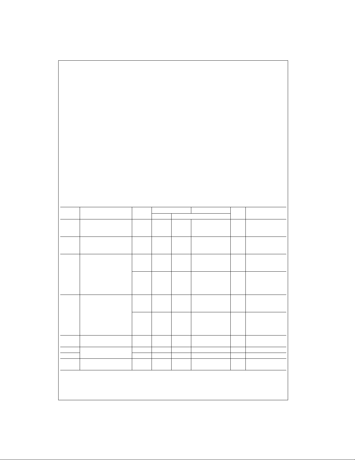
DC Electrical Characteristics for AC
V
Symbol Parameter
V
V
V
V
IIN Maximum Input
(Note 4) Leakage Current
I
OLD
I
OHD
ICC Maximum Quiescent
(Note 4) Supply Current or GND
Note 2: All outputs loaded; thres holds on input associated with output under test.
Note 3: Maximum test duration 2.0 ms, one output loaded at a time.
Note 4: I
Minimum HIGH Level 3.0 1.5 2.1 2.1 V
IH
Input Voltage 4.5 2.25 3.15 3.15 V or VCC − 0.1V
Maximum LOW Level 3.0 1.5 0.9 0.9 V
IL
Input Voltage 4.5 2.25 1.35 1.35 V or VCC − 0.1V
Minimum HIGH Level 3.0 2.99 2.9 2.9
OH
Output Voltage 4.5 4.49 4.4 4.4 V I
Maximum LOW Level 3.0 0.002 0.1 0.1
OL
Output Voltage 4.5 0.001 0.1 0.1 V I
Minimum Dynamic 5.5 75 mA V
Output Current (Note 3) 5.5 −75 mA V
and ICC @ 3.0V are guaranteed to be less than or e qual to the respective lim it @ 5. 5V VCC.
IN
CC
(V) Typ Guaranteed Limits
5.5 2.75 3.85 3.85
5.5 2.75 1.65 1.65
5.5 5.49 5.4 5.4
3.0 2.56 2.46 IOH = −12 mA
4.5 3.86 3.76 V I
5.5 4.86 4.76 I
5.5 0.001 0.1 0.1
3.0 0.36 0.44 IOL = 12 mA
4.5 0.36 0.44 V IOL = 24 mA
5.5 0.36 0.44 IOL = 24 mA (Note 2)
5.5 ±0.1 ±1.0 µAVI = VCC, GND
5.5 4.0 40.0 µA
TA = +25°CT
= −40°C to +85°C
A
Units Conditions
OUT
OUT
= −50 µA
OUT
VIN = V
= −24 mA
OH
= −24 mA (Note 2)
OH
= 50 µA
OUT
VIN = V
OLD
OHD
VIN = V
= 0.1V
= 0.1V
or V
IL
IH
or V
IL
IH
= 1.65V Max
= 3.85V Min
CC
74AC153 • 74ACT153
CC
CC
3 www.fairchildsemi.com
Page 4
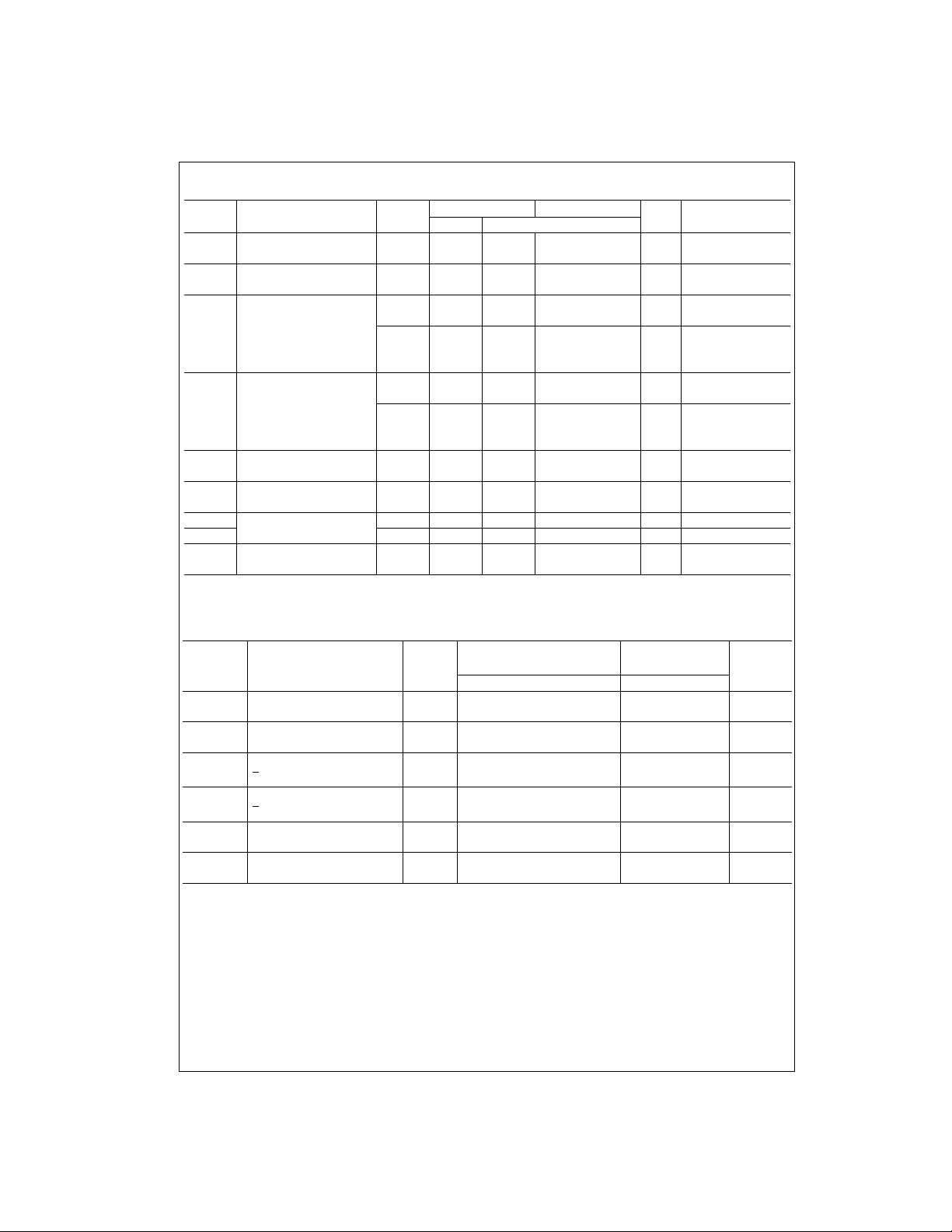
DC Electrical Characteristics for ACT
V
Symbol Parameter
V
Minimum HIGH Level 4.5 1.5 2.0 2.0
IH
CC
(V) Typ Guaranteed Limits
Input Voltage 5.5 1.5 2.0 2.0 or VCC − 0.1V
V
Maximum LOW Level 4.5 1.5 0.8 0.8
IL
Input Voltage 5.5 1.5 0.8 0.8 or V
V
74AC153 • 74ACT153
Minimum HIGH Level 4.5 4.49 4.4 4.4
OH
Output Voltage 5.5 5.49 5.4 5.4
4.5 3.86 3.76 V IOH = − 24 mA
5.5 4.86 4.76 I
V
Maximum LOW Level 4.5 0.001 0.1 0.1
OL
Output Voltage 5.5 0.001 0.1 0.1
4.5 0.36 0.44 V IOL = 24 mA
5.5 0.36 0.44 IOL = 24 mA (Note 5)
I
IN
I
CCT
I
OLD
I
OHD
I
CC
Note 5: All outputs loaded; thresholds on input associated with output under test.
Note 6: Maximum test dura tio n 2. 0 ms, one output loaded at a time.
Maximum Input
Leakage Current
Maximum
ICC/Input
5.5 ±0.1 ±1.0 µA VI = VCC, GND
5.5 0.6 1.5 mA VI = VCC − 2.1V
Minimum Dynamic 5.5 75 mA V
Output Current (Note 6) 5.5 −75 mA V
Maximum Quiescent
Supply Current or GND
5.5 4.0 40.0 µA
AC Electrical Characteristics for AC
V
CC
Symbol Parameter (V)
(Note 7) Min Typ Max Min Max
t
PLH
t
PHL
t
PLH
t
PHL
t
PLH
t
PHL
Note 7: Voltage Range 3.3 is 3.3V ± 0 3V
Propagation Delay 3.3 2.5 9.5 15.0 2.5 17.5
Sn to Z
n
5.0 2.0 6.5 11.0 2.0 12.5
Propagation Delay 3.3 3.0 8.5 14.5 2.5 16.5
Sn to Z
n
5.0 2.5 6.5 11.0 2.0 12.0
Propagation Delay 3.3 2.5 8.0 13.5 2.0 16.0
E to Z
n
5.0 1.5 5.5 9.5 1.5 11.0
Propagation Delay 3.3 2.5 7.0 11.0 2.0 12.5
E to Z
n
5.0 2.0 5.0 8.0 1.5 9.0
Propagation Delay 3.3 2.5 7.5 12.5 2.0 14.5
In to Z
n
5.0 1.5 5.5 9.0 1.5 10.5
Propagation Delay 3.3 1.5 7.0 11.5 1.5 13.0
In to Z
n
Voltage Range 5.0 is 5.0V ± 0.5V
5.0 1.5 5.0 8.5 1.5 10.0
TA = +25°CT
= −40°C to +85°C
A
TA = +25°CT
C
= 50 pF CL = 50 pF
L
Units Conditions
V
= 0.1V
OUT
V
V
= 0.1V
OUT
V
V I
V I
= −40°C to +85°C
A
− 0.1V
CC
= −50 µA
OUT
VIN = V
or V
IL
= − 24 mA (Note 5)
OH
= 50 µA
OUT
VIN = V
or V
IL
= 1.65V Max
OLD
= 3.85V Min
OHD
VIN = V
CC
IH
IH
Units
ns
ns
ns
ns
ns
ns
www.fairchildsemi.com 4
Page 5
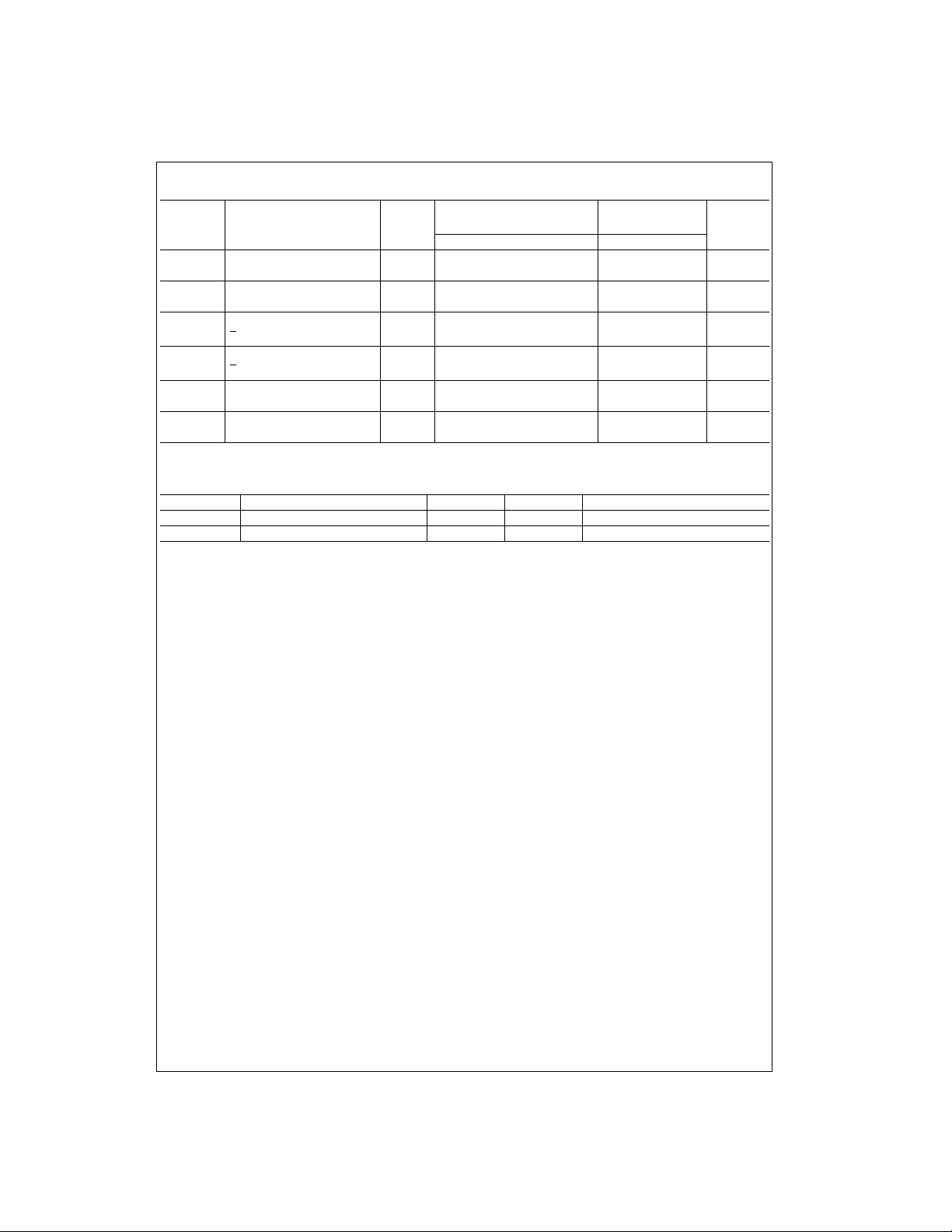
AC Electrical Characteristics for ACT
Symbol Parameter (V)
t
PLH
t
PHL
t
PLH
t
PHL
t
PLH
t
PHL
Note 8: Voltage Range 5.0 is 5.0V ± 0.5V
Propagation Delay
to Z
S
n
n
Propagation Delay
S
to Z
n
n
Propagation Delay
En to Z
n
Propagation Delay
En to Z
n
Propagation Delay
to Z
I
n
n
Propagation Delay
I
to Z
n
n
V
CC
(Note 8) Min Typ Max Min Max
5.0 3.0 7.0 11.5 2.0 13.5 ns
5.0 3.0 7.0 11.5 2.5 13.5 ns
5.0 2.0 6.5 10.5 2.0 12.5 ns
5.0 3.0 6.0 9.5 2.5 11.0 ns
5.0 2.5 5.5 9.5 2.0 11.0 ns
5.0 2.0 5.5 9.5 2.0 11.0 ns
TA = +25°CT
C
= 50 pF CL = 50 pF
L
= −40°C to +85°C
A
Capacitance
Symbol Parameter Typ Un its Conditions
C
IN
C
PD
Input Capacitance 4.5 pF VCC = OPEN
Power Dissipation Capacitance 65.0 pF VCC = 5.0V
74AC153 • 74ACT153
Units
5 www.fairchildsemi.com
Page 6
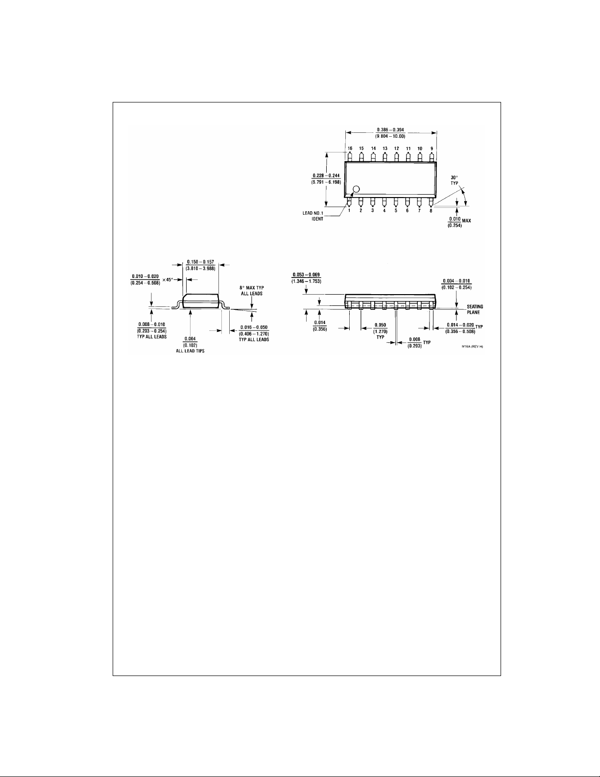
Physical Dimensions inches (millimeters) unless otherwise noted
74AC153 • 74ACT153
16-Lead Small Outline Integrated Circuit (SOIC), JEDEC MS -012, 0.150” Narrow Body
Package Number M16A
www.fairchildsemi.com 6
Page 7
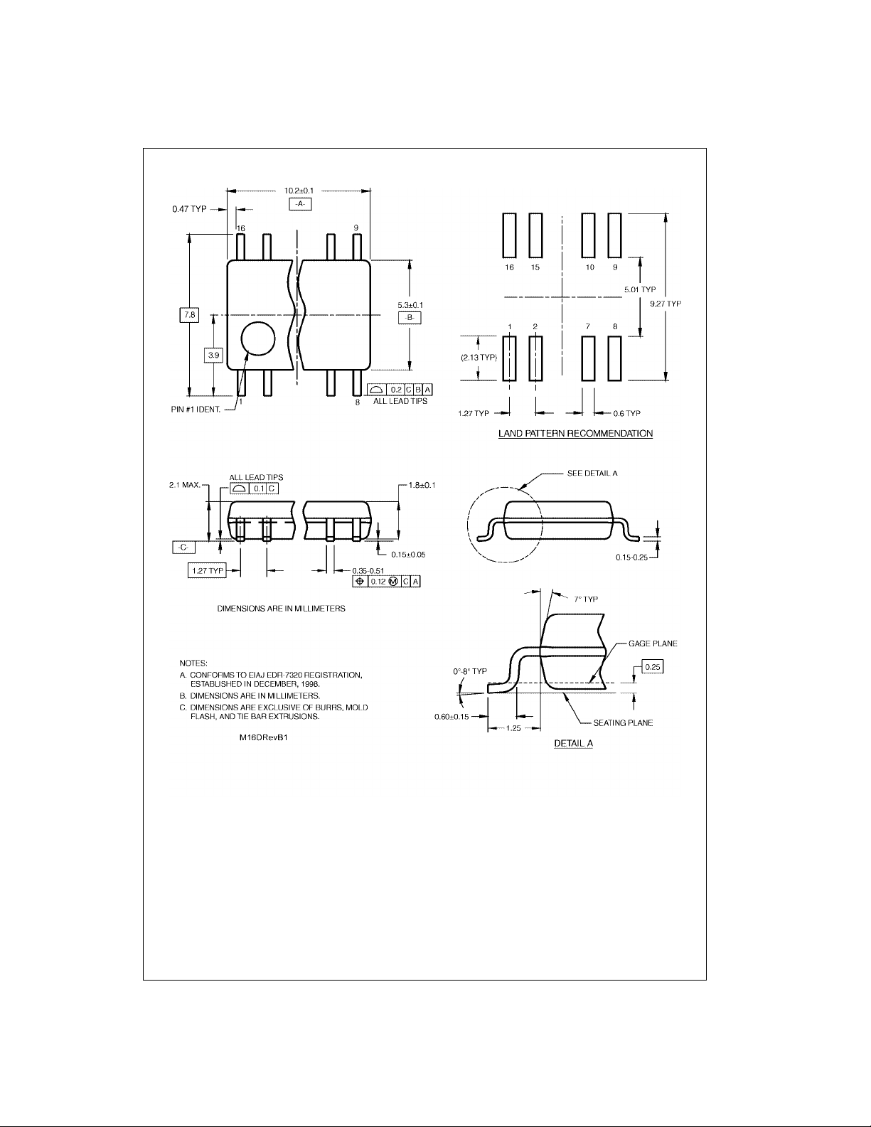
Physical Dimensions inches (millimeters) unless otherwise noted (Continued)
74AC153 • 74ACT153
16-Lead Small Outline Package (SOP), EIAJ TYPE II, 5.3mm Wide
Package Number M16D
7 www.fairchildsemi.com
Page 8
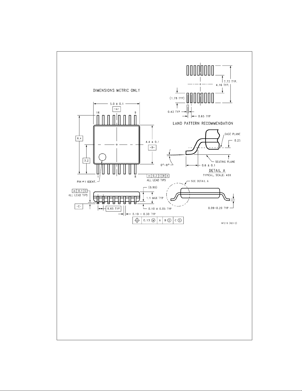
Physical Dimensions inches (millimeters) unless otherwise noted (Continued)
74AC153 • 74ACT153
16-Lead Thin Shrink Small Outline Package (TSSOP), JEDEC MO-153, 4.4mm Wide
www.fairchildsemi.com 8
Package Number MTC16
Page 9
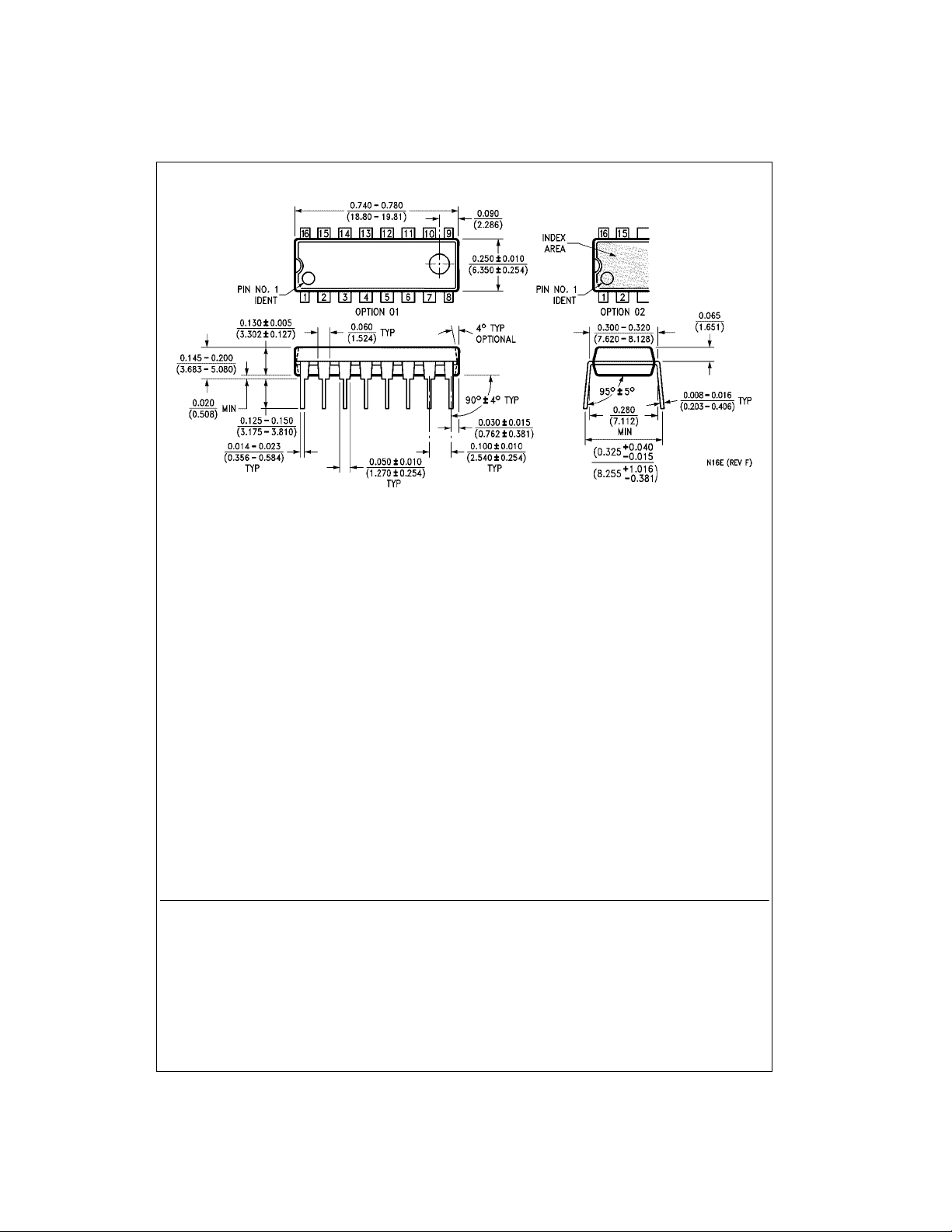
Physical Dimensions inches (millimeters) unless otherwise noted (Continued)
74AC153 • 74ACT153 Dual 4-Input Multiplexer
16-Lead Plastic Dual-In-Line Package (PDIP), JEDEC MS-001, 0.300” Wide
Fairchild does not assume any responsibility for use of any circuitry described , no circuit patent licenses are implied and
Fairchild reserves the right at any time without notice to change said circuitry and specifications.
LIFE SUPPORT POLICY
FAIRCHILD’S PRODUCTS ARE NOT AUTHORIZED FOR USE AS CRITICAL COMPONENTS IN LIFE SUPPORT
DEVICES OR SYSTEMS WITHOUT THE EXPRESS WRITTEN APPROVAL OF THE PRESIDENT OF FAIRCHILD
SEMICONDUCTOR CORPORATION. As used herein:
1. Life support devices or systems are dev ic es or syste ms
which, (a) are intended for surgical implant into the
body, or (b) support or sustain life, and (c) whose failure
to perform when properly used in accordance with
instructions for use provide d in the l abe ling, can be reasonably expected to result in a significant injury to the
user.
Package Number N16E
2. A critical compo nent in any com ponen t of a life s upp ort
device or system whose failure to perform can be reasonably expected to cause the failure of the life support
device or system, or to affect its safety or effectiveness.
www.fairchildsemi.com
9 www.fairchildsemi.com
 Loading...