

Page 1
74AC14
HEX SCHMITT INVERT ER
■ HIGH SPEED: t
■ LOW POWER DISSIPATION:
I
= 4µA(MAX.) at TA=25°C
CC
■ 50Ω TRASMISSION LINE DRIVING
= 4.5ns (TYP.) at VCC = 5V
PD
CAPABILITY
■ SYMMETRICAL OUTPUT IMPEDANCE:
|I
| = IOL = 24mA (MIN)
OH
■ BALANCED PROPAGATION DELAYS:
t
≅ t
PLH
■ OPERATING VOLTAGE RANGE:
V
CC
■ PIN AND FUNCTION COMPATIBLE WITH
PHL
(OPR) = 2V to 6V
74 SERIES 14
■ IMPROVED LATCH-UP IMMUNITY
DESCRIPTION
The 74AC14 is an advanced high-speed CMOS
HEX SCHMITT TRIGGER INVERTER fabricated
with sub-micron silicon gate and double-layer
metal wiring C
2
MOS technology.
The internal circuit is composed of 3 stages
including buffer output , which enables high noise
immunity and stable output.
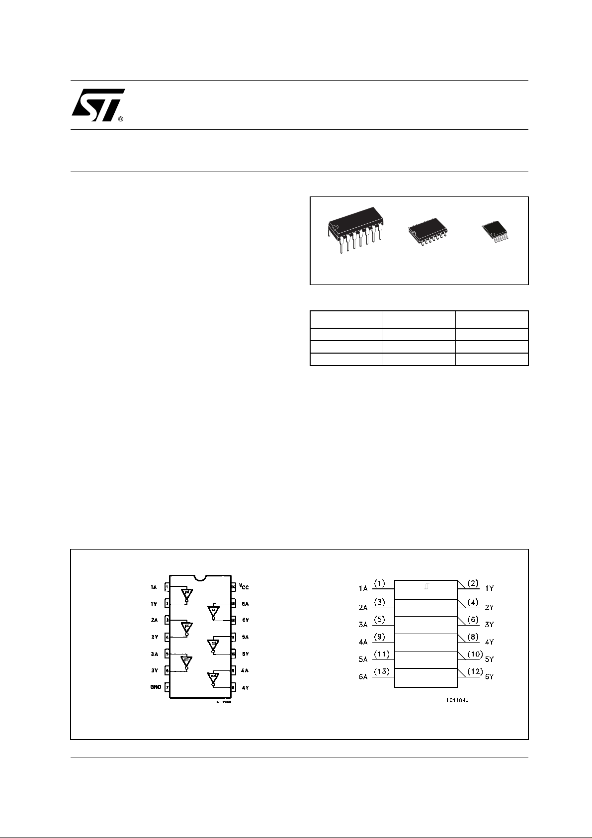
TSSOPDIP SOP
ORDER CODES
PACKAGE TUBE T & R
DIP 74AC14B
SOP 74AC14M 74AC14MTR
TSSOP 74AC14TTR
This together with its schmitt trigger function
allows it to be used on line receivers with slow
rise/fall input signals.
All inputs and outputs are equipped with
protection circuits against stat ic discharge, giving
them 2KV ESD immunity and transient excess
voltage.
PIN CONNECTION AND IEC LOGIC SYMBOLS
1/8July 2001
Page 2
74AC14
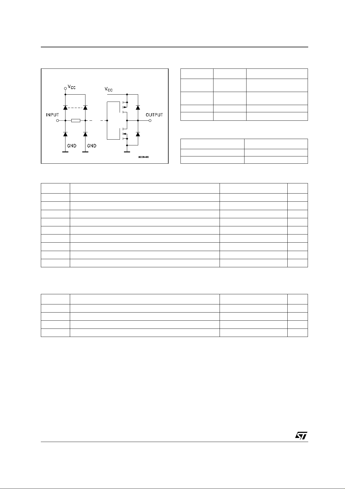
INPUT AND OUTPUT EQUIVALENT CIRCUIT PIN DESCRIPTION
PIN No SYMBOL NAME AND FUNCTION
1, 3, 5, 9, 1 1,
13
2, 4, 6, 8, 10,
12
7 GND Ground (0V)
14
TRUTH TABLE
ABSOLUTE MAXIMUM RATINGS
Symbol Parameter Value Unit
V
V
V
I
I
OK
I
I
or I
CC
T
T
Absolute Maximum Ratings are those values beyond which damage to the device may occur. Functional operation under these conditions is
not implied.
Supply Voltage
CC
DC Input Voltage -0.5 to VCC + 0.5
I
DC Output Voltage -0.5 to VCC + 0.5
O
DC Input Diode Current
IK
DC Output Diode Current
DC Output Current
O
DC VCC or Ground Current
GND
Storage Temperature
stg
Lead Temperature (10 sec)
L
1A to 6A Data Inputs
1Y to 6Y Data Outputs
V
CC
Positive Supply Voltage
AY
LH
HL
-0.5 to +7 V
V
V
± 20 mA
± 20 mA
± 50 mA
± 300 mA
-65 to +150 °C
300 °C
RECOMMENDED OPERATING CONDITIONS
Symbol Parameter Value Unit
V
V
V
T
2/8
Supply Voltage
CC
Input Voltage 0 to V
I
Output Voltage 0 to V
O
Operating Temperature
op
2 to 6 V
CC
CC
-55 to 125 °C
V
V
Page 3
DC SPECIFICATIONS
Test Condition Value
T
Symbol Parameter
V
CC
(V)
V
High Level Input
t+
Voltage
3.0
T
=Worst Case
A
5.5 3.9 3.9 3.9
V
t-
Low Level Input
Voltage
3.0
T
=Worst Case
A
5.5 1.1 1.1 1.1
Hysteresis Voltage 3.0
V
h
T
=Worst Case
A
5.5 0.5 1.6 0.5 1.6 1.6
V
High Level Output
OH
Voltage
3.0
4.5
5.5
3.0
4.5
5.5
V
Low Level Output
OL
Voltage
3.0
4.5
5.5
3.0
4.5
5.5
I
Input Leakage Cur-
I
rent
I
I
OLD
I
OHD
1) Maxim um test duration 2ms, one output loaded at tim e
2) Incid ent wave switching is guaranteed on transmission l i nes with impe dances as low as 50Ω
Quiescent Supply
CC
Current
Dynamic Output
Current (note 1, 2)
5.5
5.5
5.5
=-50 µA
I
O
I
=-50 µA
O
I
=-50 µA
O
I
=-12 mA
O
I
=-24 mA
O
I
=-24 mA
O
IO=50 µA
I
=50 µA
O
I
=50 µA
O
I
=12 mA
O
I
=24 mA
O
I
=24 mA
O
= VCC or GND
V
I
= VCC or GND
V
I
= 1.65 V max
V
OLD
V
= 3.85 V min
OHD
= 25°C
A
Min. Typ. Max. Min. Max. Min. Max.
2.2 2.2 2.2
0.5 0.5 0.5
0.3 1.2 0.3 1.2 1.2
2.9 2.99 2.9 2.9
4.4 4.49 4.4 4.4
5.4 5.49 5.4 5.4
2.56 2.46 2.46
3.86 3.76 3.76
4.86 4.76 4.76
0.002 0.1 0.1 0.1
0.001 0.1 0.1 0.1
0.001 0.1 0.1 0.1
0.36 0.44 0.44
0.36 0.44 0.44
0.36 0.44 0.44
± 0.1 ± 1 ± 1 µA
44040µA
74AC14
-40 to 85°C -55 to 125°C
75 50 mA
-75 -50 mA
Unit
V4.5 3.2 3.2 3.2
V4.5 0.9 0.9 0.9
V4.5 0.4 1.4 0.4 1.4 1.4
V
V
AC ELECTRICAL CHARACTERISTICS (CL = 50 pF, RL = 500 Ω, Input tr = tf = 3ns)
Test Condition Value
= 25°C
Symbol Parameter
t
PLH tPHL
(*) Vol tage range is 3.3V ± 0.3V
(**) Voltage range is 5.0V ±
Propagation Delay
Time
0.5V
V
3.3
5.0
(V)
CC
(*)
(**)
T
A
Min. Typ. Max. Min. Max. Min. Max.
1.5 6.0 11.0 1.0 15.0 1.0 16.0
1.5 4 8.0 1.0 11.0 1.0 12.0
-40 to 85°C -55 to 125°C
Unit
ns
3/8
Page 4

74AC14
CAPACITIVE CHARACTERISTICS
Test Condition Value
T
Symbol Parameter
C
C
Input Capacitance
IN
Power Dissipation
PD
Capacitance
V
CC
(V)
5.0 4 pF
5.0
= 10MHz
f
IN
= 25°C
A
Min. Typ. Max. Min. Max. Min. Max.
35 pF
(note 1)
1) CPD is defined as the value of the IC’s internal equivalent capacitance which is calculated from the operating current consumption without
load. (Refer to Test Circuit). Average operating current can be obtained by the following equation. I
TEST CIRCUIT
-40 to 85°C -55 to 125°C
= CPD x VCC x fIN + ICC/6 (per gate)
CC(opr)
Unit
CL = 50pF or equivalent (includes jig and probe capacitance)
= R1 = 500Ω or equivalent
R
L
= Z
R
of pulse generator (typically 50Ω)
T
OUT
WAVEFORM: PROPAGATION DELAYS (f=1MHz; 50% duty cycle)
4/8
Page 5

Plastic DIP-14 MECHANICAL DATA
mm. inch
DIM.
MIN. TYP MAX. MIN. TYP. MAX.
a1 0.51 0.020
B 1.39 1.65 0.055 0.065
b 0.5 0.020
b1 0.25 0.010
D 20 0.787
E 8.5 0.335
e 2.54 0.100
e3 15.24 0.600
F 7.1 0.280
74AC14
I 5.1 0.201
L 3.3 0.130
Z 1.27 2.54 0.050 0.100
P001A
5/8
Page 6

74AC14
SO-14 MECHANICAL DATA
DIM.
A 1.75 0.068
a1 0.1 0.2 0.003 0.007
a2 1.65 0.064
b 0.35 0.46 0.013 0.018
b1 0.19 0.25 0.007 0.010
C 0.5 0.019
c1 45° (typ.)
D 8.55 8.75 0.336 0.344
E 5.8 6.2 0.228 0.244
e 1.27 0.050
e3 7.62 0.300
F 3.8 4.0 0.149 0.157
G 4.6 5.3 0.181 0.208
L 0.5 1.27 0.019 0.050
M 0.68 0.026
S8° (max.)
MIN. TYP MAX. MIN. TYP. MAX.
mm. inch
6/8
PO13G
Page 7

74AC14
TSSOP14 MECHANICAL DATA
mm. inch
DIM.
MIN. TYP MAX. MIN. TYP. MAX.
A 1.2 0.047
A1 0.05 0.15 0.002 0.004 0.006
A2 0.8 1 1.05 0.031 0.039 0.041
b 0.19 0.30 0.007 0.012
c 0.09 0.20 0.004 0.0089
D 4.9 5 5.1 0.193 0.197 0.201
E 6.2 6.4 6.6 0.244 0.252 0.260
E1 4.3 4.4 4.48 0.169 0.173 0.176
e 0.65 BSC 0.0256 BSC
K0° 8°0° 8°
L 0.45 0.60 0.75 0.018 0.024 0.030
A2
A
A1
b
e
c
K
L
E
D
E1
PIN 1 IDENTIFICATION
1
0080337D
7/8
Page 8

74AC14
Information furnished is bel ieved to be accurate and reliable. However, STMicroe lectronics assumes no responsibility for the
consequences of use of such information nor for any infringement of patents or other rights of third parties which may result from
its use. No li cense is granted by implica tion or otherwise under any patent or patent righ ts of S TMic roelec tronics. Specifications
mentioned in this publication ar e subject to change without notice. This publication supersedes and replaces all information
previously supplied. S TMicroelectronics products are not authorized for use as critica l components in life suppo rt devices or
systems without express written approval of STMicroelectronics.
Australi a - Brazil - China - Finland - France - Germany - Hong Kong - India - Italy - Japan - Malay sia - Malta - Morocco
© The ST logo is a registered trademark of STMicroelectronics
© 2001 STM icroelectronics - Prin ted in Italy - All Rights Reserved
STMicr o el ectronics GROU P OF COMPANIE S
Singapo re - Spain - Swe den - Switzerl and - United K i ngdom
© http://www.st.com
8/8
 Loading...