

Page 1
74AC14
HEX INVERTER
■ HIGH SPEED: t
■ LOWPOWERDISSIPATION:
I
=4µA (MAX.) at TA=25oC
CC
■ HIGH NOISE IMMUNITY:
V
NIH=VNIL
■ 50Ω TRANSMISSIONLINE DRIVING
=6 ns(TYP.)atVCC=3.3V
PD
=28%VCC(MIN.)
CAPABILITY
■ SYMMETRICAL OUTPUT IMPEDANCE:
|=IOL=24mA (MIN)
|I
OH
■ BALANCEDPROPAGAT IOND ELAY S:
t
≅ t
PLH
PHL
■ OPERATINGVOLTAGER ANGE:
V
(OPR) = 2V to 6V
CC
■ PIN AND FUNCTION COMPATIBLE WITH
74SERIES14
■ IMPROVED LATCH-UP IMMUNITY
DESCRIPTION
The AC14 is an advanced high-speed CMOS
HEX INVERTER fabricated with sub-micron
silicon gateand double-layermetal wiring C
2
MOS
technology. It is ideal for low power applications
mantaining high speed operation similar to
B
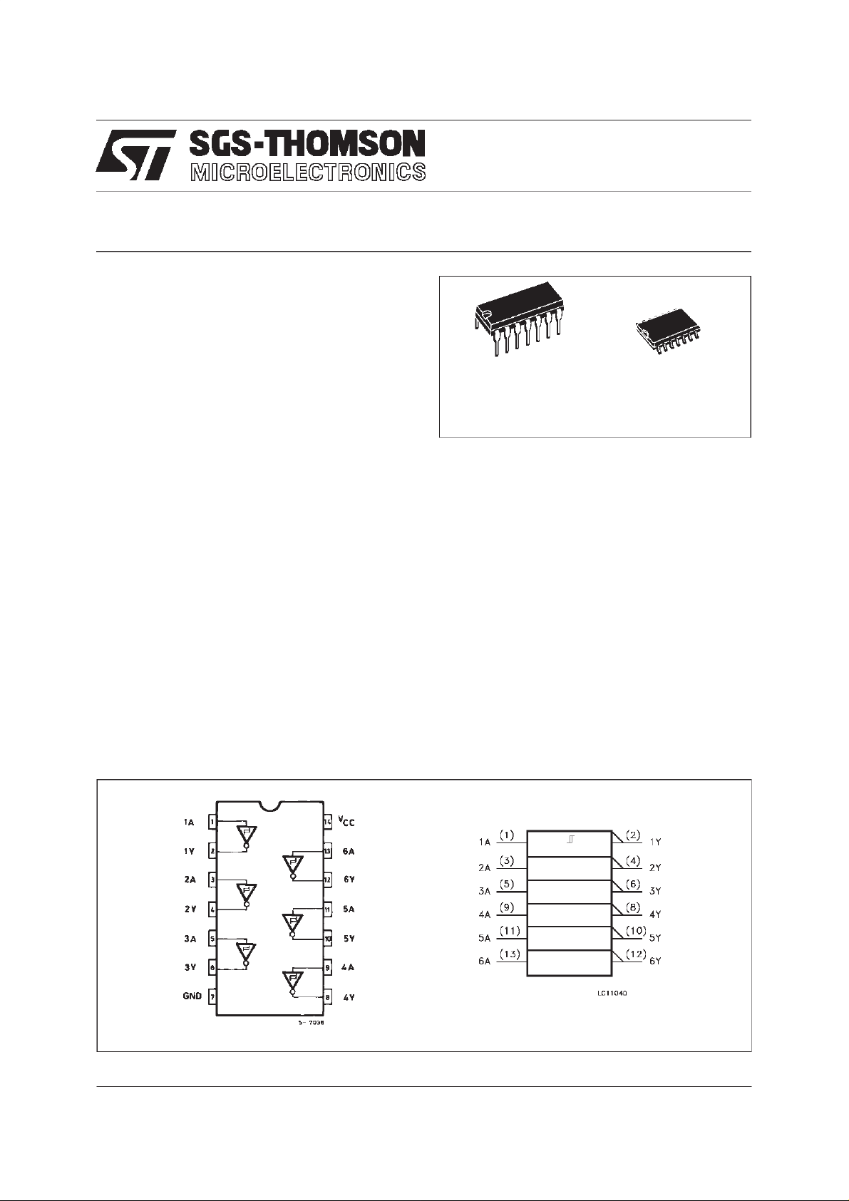
(Plastic Package)
(Micro Package)
M
ORDERCODES :
74AC14B 74AC14M
equivalentBipolarShottky TTL.
The internal circuit is composed of 3 stages
including buffer output, which enables high noise
immunityand stable output.
This together with its schmitt trigger function
allows it to be used on line receivers with slow
rise/fallinputsegnals.
All inputs and outputs are equipped with
protectioncircuits against static discharge, giving
them 2KV ESD immunity and transient excess
voltage.
PINCONNECTION ANDIEC LOGIC SYMBOLS
March 1998
1/7
Page 2
74AC14
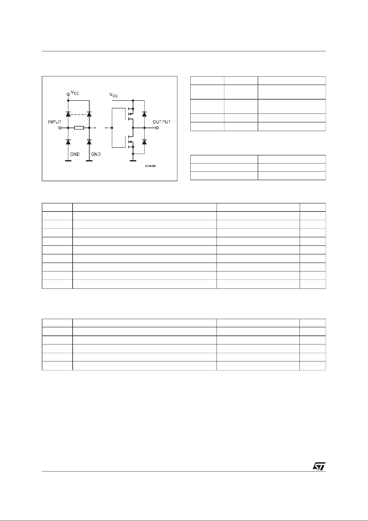
INPUTAND OUTPUT EQUIVALENTCIRCUIT
PIN DESCRIPTION
PI N No SYM B O L NAME AND F UNC T I ON
1, 3, 5, 9,
1A to 6A Data Inputs
11, 13
2, 4, 6, 8,
1Y to 6Y Data Oututs
10, 12
7 GND Ground (0V)
14 V
CC
Positive Supply Voltage
TRUTHTABLE
AY
LH
HL
ABSOLUTE MAXIMUM RATINGS
Symb o l Parame t er Val u e Uni t
V
V
V
I
I
OK
I
orI
I
CC
T
T
Absolute Maximum Ratings are those values beyond which damage to the device may occur. Functional operation under these condition is not implied.
Supply Voltage -0.5 to +7 V
CC
DC Input Voltage -0.5 to VCC+ 0.5 V
I
DC Output Voltage -0.5 to VCC+ 0.5 V
O
DC Input Diode Current ± 20 mA
IK
DC Output Diode Current ± 20 mA
DC Output Current ± 50 mA
O
DC VCCor Ground Current ± 300 mA
GND
Storage Temperature -65 to +150
stg
Lead Temperature (10 sec) 300
L
o
C
o
C
RECOMMENDED OPERATING CONDITIONS
Symb o l Parame t er Value Un i t
V
V
V
T
dt/dv Input Rise and Fall Time V
1) VINfrom30% to70%of V
2/7
Supply Voltage 2 to 6 V
CC
Input Voltage 0 to V
I
Output Voltage 0 to V
O
Operating Temperature: -40 to +85
op
= 3.0, 4.5 or 5.5 V(note 1) 8 ns/V
CC
CC
CC
CC
V
V
o
C
Page 3
DC SPECIFICATIONS
74AC14
Symbol Parameter Test Condition s Value Unit
T
V
CC
(V)
High Level Input Voltage 3.0 TA= Worst Case 2.2 2.2
V
t+
=25oC-40to85
A
Min. Ty p. Ma x. Min. Max.
o
C
4.5 3.2 3.2
5.5 3.9 3.9
Low Level Input Voltage 3.0 TA= Worst Case 0.5 0.5
V
t-
4.5 0.9 0.9
5.5 1.1 1.1
Hysteresis Voltage 3.0 TA= Worst Case 0.3 1.2 0.3 1.2
V
h
4.5 0.4 1.4 0.4 1.4
5.5 0.5 1.6 0.5 1.6
High Level Output
V
OH
Voltage
Low Level Output
V
OL
Voltage
Input Leakage Current
I
I
Quiescent Supply
I
CC
3.0
4.5 I
5.5 I
V
V
3.0 I
4.5 I
5.5 I
3.0
4.5 I
5.5 I
V
V
3.0 I
4.5 I
5.5 I
5.5
IO=-50 µA 2.9 2.99 2.9
(*)
I
IH
V
IL
=-50 µA 4.4 4.49 4.4
O
=
or
=-50 µA 5.4 5.49 5.4
O
=-12 mA 2.56 2.46
O
=-24 mA 3.86 3.76
O
=-24 mA 4.86 4.76
O
IO=50 µA 0.002 0.1 0.1
(*)
I
IH
V
IL
=50 µA 0.001 0.1 0.1
O
=
or
=50 µA 0.001 0.1 0.1
O
=12 mA 0.36 0.44
O
=24 mA 0.36 0.44
O
=24 mA 0.36 0.44
O
VI=VCCor GND ±0.1 ±1 µA
5.5 VI=VCCor GND 4 40 µA
Current
Dynamic Output Current
I
OLD
OHD
(note 1, 2)
I
1) Maximum test duration 2ms, one output loaded at time
2) Incident wave switching is guaranteed on transmission lines with impedances as low as 50 Ω.
5.5 V
= 1.65 V max 75 mA
OLD
V
= 3.85 V min -75 mA
OHD
V
V
V
V
V
AC ELECTRICAL CHARACTERISTICS (CL= 50 pF, RL=500 Ω, Inputtr=tf=3ns)
Symbol Parameter Test Conditi on Value Unit
t
Propagation Delay Time 3.3
PLH
t
PHL
(*) Voltagerange is3.3V ± 0.3V
(**) Voltage range is5V ± 0.5V
V
5.0
CC
(V)
(*)
(**)
T
=25oC-40to85
A
Min. Ty p. Ma x. Min. Max.
1.5 6 11 1 13
1.5 4.5 8 1 9
o
C
ns
3/7
Page 4

74AC14
CAPACITIVE CHARACTERISTICS
Symbol Parameter Test Condition s Value Unit
V
CC
(V)
Input Capacitance 5.0 4 pF
C
IN
Power Dissipation
C
PD
5.0 35 pF
=25oC-40to85
T
A
Min. Ty p. Ma x. Min. Max.
o
C
Capacitance (note 1)
1) CPDis defined as the value of the IC’s internal equivalent capacitance which is calculated from the operating current consumption without load. (Refer to
Test Circuit). Average operating current can be obtained by the following equation. I
(opr) = CPD• VCC• fIN+ICC/n (per circuit)
CC
TEST CIRCUIT
CL= 50 pF or equivalent (includes jig and probe capacitance)
R
= 500Ω or equivalent
L=R1
R
of pulse generator (typically 50Ω)
T=ZOUT
WAVEFORM: PROPAGATION DELAYS (f=1MHz)
4/7
Page 5

Plastic DIP-14 MECHANICALDATA
74AC14
DIM.
MIN. TYP. MAX. MIN. TYP. MAX.
a1 0.51 0.020
B 1.39 1.65 0.055 0.065
b 0.5 0.020
b1 0.25 0.010
D 20 0.787
E 8.5 0.335
e 2.54 0.100
e3 15.24 0.600
F 7.1 0.280
I 5.1 0.201
L 3.3 0.130
Z 1.27 2.54 0.050 0.100
mm inch
P001A
5/7
Page 6

74AC14
SO-14 MECHANICALDATA
DIM.
MIN. TYP. MAX. MIN. TYP. MAX.
A 1.75 0.068
a1 0.1 0.2 0.003 0.007
a2 1.65 0.064
b 0.35 0.46 0.013 0.018
b1 0.19 0.25 0.007 0.010
C 0.5 0.019
c1 45 (typ.)
D 8.55 8.75 0.336 0.344
E 5.8 6.2 0.228 0.244
e 1.27 0.050
e3 7.62 0.300
F 3.8 4.0 0.149 0.157
G 4.6 5.3 0.181 0.208
L 0.5 1.27 0.019 0.050
M 0.68 0.026
S 8 (max.)
mm inch
6/7
P013G
Page 7

74AC14
Information furnished is believed to be accurate and reliable. However, SGS-THOMSON Microelectronics assumes no responsabilityfor the
consequences of use of such information nor for any infringement ofpatents or otherrights of thirdparties which may results from its use.No
license isgranted by implication or otherwise underanypatentor patentrights of SGS-THOMSON Microelectronics.Specifications mentioned
in this publication are subjectto change without notice. This publication supersedes and replacesall information previouslysupplied.
SGS-THOMSON Microelectronics products arenot authorized for useascritical components inlifesupport devices orsystems withoutexpress
writtenapproval of SGS-THOMSON Microelectonics.
1998 SGS-THOMSON Microelectronics - Printed in Italy - AllRights Reserved
Australia - Brazil - Canada - China - France -Germany -Hong Kong - Italy - Japan - Korea - Malaysia - Malta - Morocco- The Netherlands -
Singapore - Spain - Sweden - Switzerland -Taiwan - Thailand - United Kingdom - U.S.A
SGS-THOMSON Microelectronics GROUP OF COMPANIES
.
7/7
 Loading...