

Datasheet 74ABT652CMTC, 74ABT652CMSAX, 74ABT652CMSA, 74ABT652CSPC, 74ABT652CSCX Datasheet (Fairchild Semiconductor)
...Page 1
November 1992
Revised January 1999
74ABT652 Octal Transceivers and Registers with 3-STATE Outputs
© 1999 Fairchild Semiconductor Corporation DS011512.prf www.fairchildsemi.com
74ABT652
Octal Transceiver s and Registe rs with 3-STATE Output s
General Description
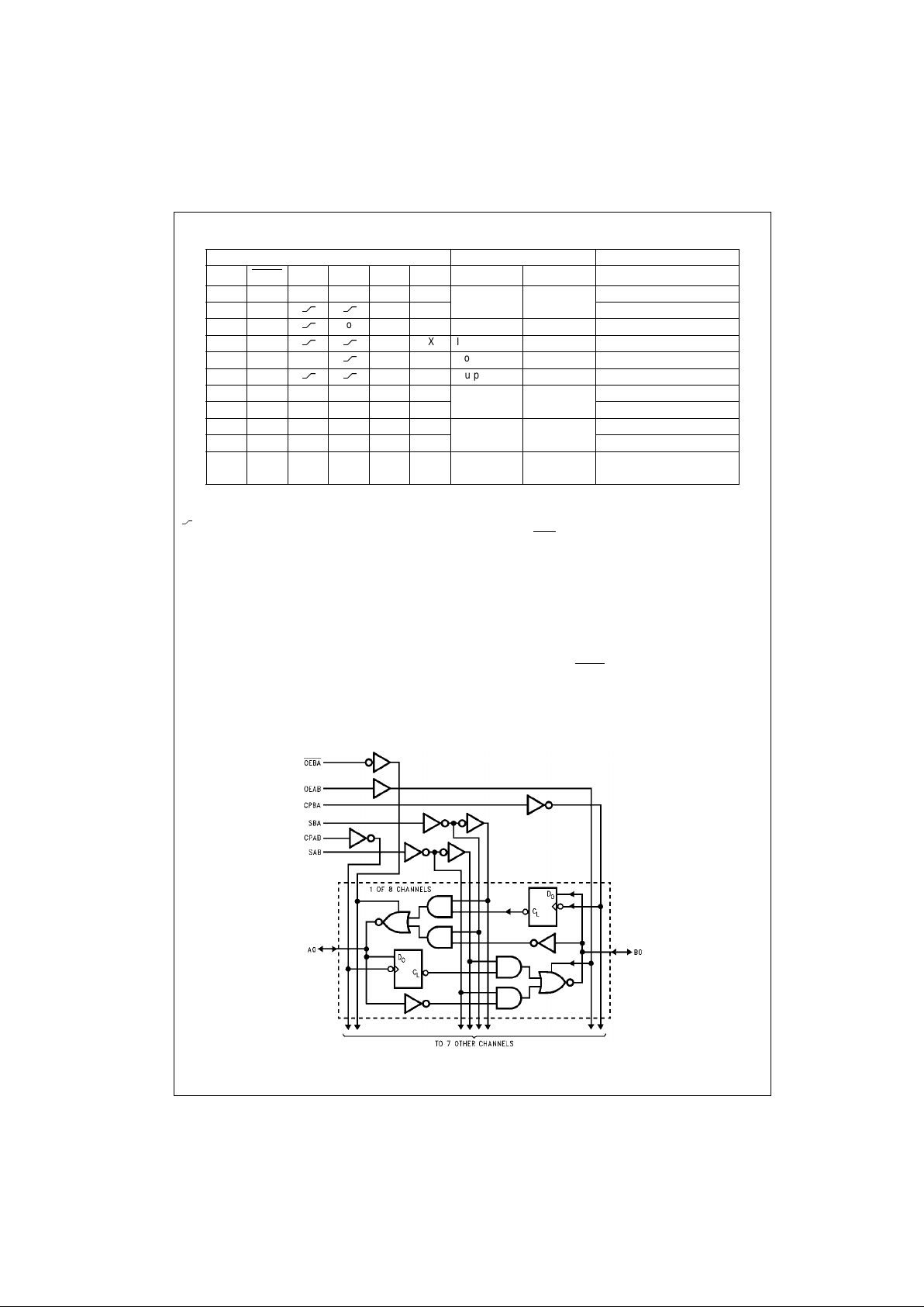
The ABT652 consists of bus transceiver circuits with Dtype flip-flops and cont rol circu itr y arrang ed for multip lexed
transmission of data directl y from th e input bus or fr om the
internal registers. Data on the A or B bus will be clocked
into the registers as the appropriate clock pin goes to HIGH
logic level. Output Enable pins (OEAB, OEBA
) are pro-
vided to control the transceiver function.
Features
■ Independent registers for A and B buses
■ Multiplexed real-time and stored data
■ A and B output sink capability of 64 mA, source
capability of 32 mA
■ Guaranteed output skew
■ Guaranteed multiple output switching specifications
■ Output switching specified for both 50 pF and
250 pF loads
■ Guaranteed simultaneous switching noise level and
dynamic threshold performance
■ Guaranteed latchup protection
■ High impedance glitch free bus loading during entire
power up and power down cycle
■ Nondestructive hot insertion capability
Ordering Code:
Devices also available in Tape and Reel. Specify by appending the suffix letter “X” to t he ordering code.
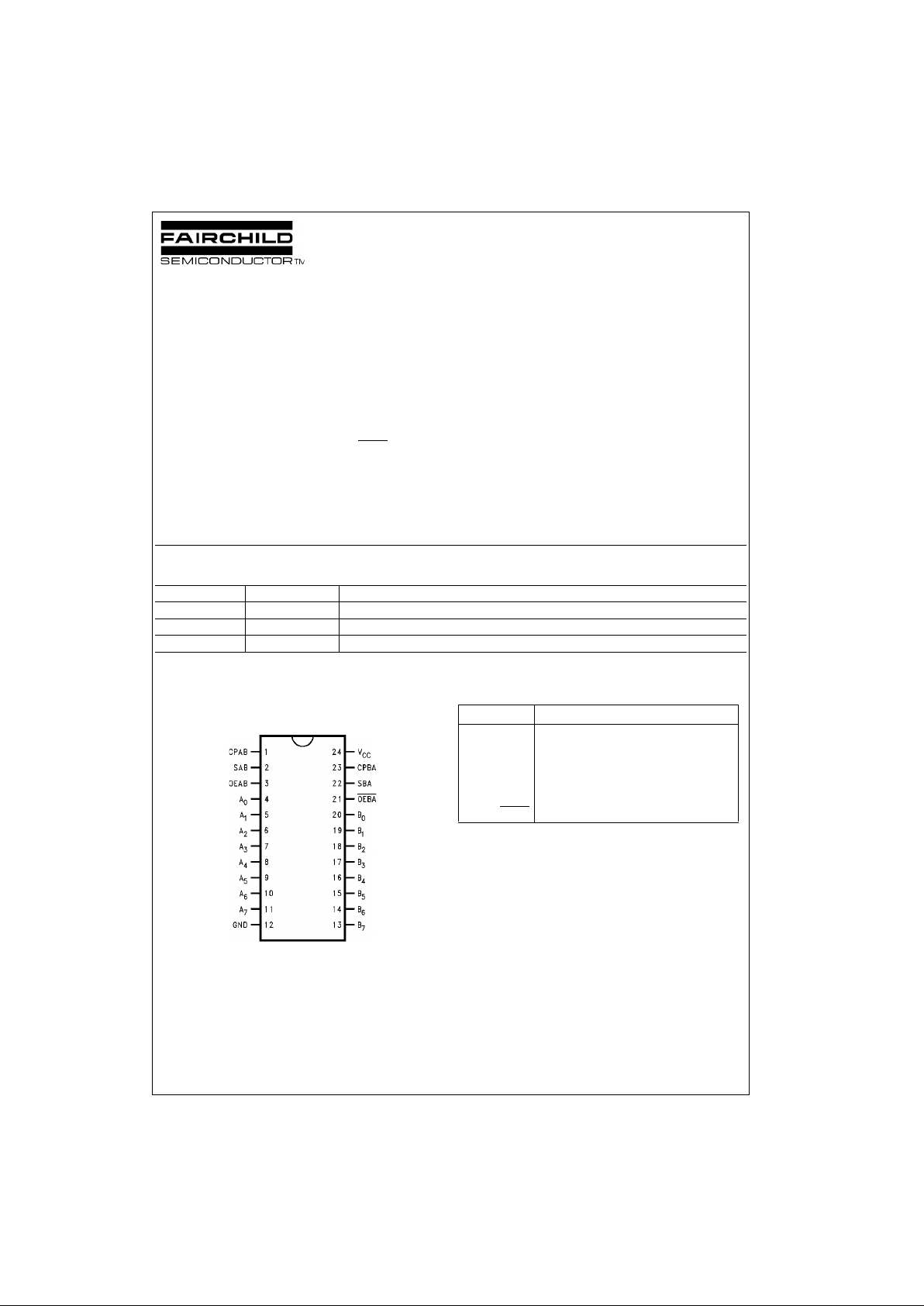
Connection Diagram
Pin Assignment for
SOIC, SSOP and TSSOP
Pin Descriptions
Order Number Package Number Package Description
74ABT652CSC M24B 24-Lead Small Outline Integrated Circuit (SOIC), JEDEC MS-013, 0.300” Wide Body
74ABT652CMSA MSA24 24-Lead Shrink Small Outline Package (SSOP), EIAJ TYPE II, 5.3mm Wide
74ABT652CMTC MTC24 24-Lead Thin Shrink Small Outline Package (TSSOP), JEDEC MO-153, 4.4mm Wide
Pin Names Description
A
0–A7
Data Register A Inputs/3-STATE Outputs
B
0–B7
Data Register B Inputs/3-STATE Outputs
CPAB, CPBA Clock Pulse Inputs
SAB, SBA Select Inputs
OEAB, OEBA
Output Enable Inputs
Page 2
www.fairchildsemi.com 2
74ABT652
Truth Table
H = HIGH Voltage Level
L = LOW V oltage Leve l
X = Immaterial
= LOW to HIGH Clock Transition
Note 1: The data output f unction s may be enabled or dis abled by vario us si gnals a t OEA B or OE BA
inputs. Data input functions are always enabled, i.e.,
data at the bus pins will b e s to red on every LOW to HIGH transition on the clock inputs.
Functional Description
In the transceiver mo de, data presen t at the HI GH impedance port may be stored in either the A or B register or
both.
The select (SAB, SBA) controls can multiplex stored and
real-time.
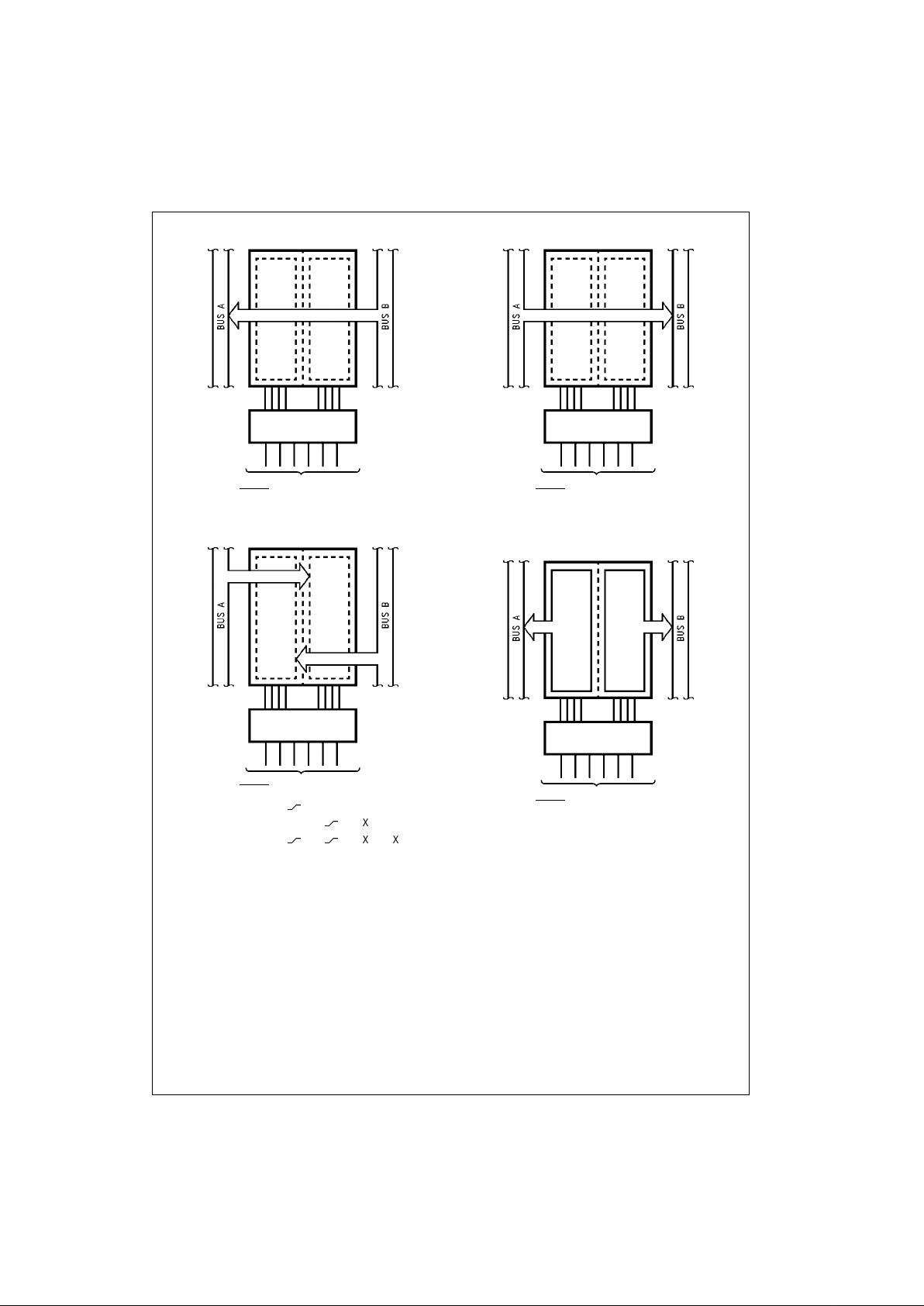
The examples in Figure 1 demon strate th e four fundamen tal bus-management func tions that can be perfor med with
the ABT652.
Data on the A or B data bus, or both, can be stored in the
internal D flip-flop by LOW to HIGH transitions at the
appropriate Clock Inpu ts (CPAB, CPBA) regardless o f the
Select or Output Enable Inputs. When SAB and SBA are in
the real time transfer mod e, it is also possible to store data
without using the internal D flip-flops by simultaneously
enabling OEAB and OEBA
. In this configuration each Output reinforces its Input. Thus when all other data sources to
the two sets of bus lines are i n a HIGH impedance sta te,
each set of bus lines will remain at its last state.
Logic Diagram
Please note that this diagram is provided only for the understanding of logic operations and should not be used to estimate propagation delays.
Inputs Inputs/Outputs (Note 1) Operating Mode
OEAB
OEBA
CP AB CPBA SAB SBA
A
0
thru A7 B0 thru B
7
L H H or L H or L X X Input Input Isolation
L H
X X Store A and B Data
X H
H or L X X Input Not Specified Store A, Hold B
H H
X X Input Output Store A in Both Registers
L X H or L
X X Not Specified Input Hold A, Store B
L L
X X Output Input Store B in Both Registers
L L X X X L Output Input Real-Time B Data to A Bus
L L X H or L X H Store B Data to A Bus
H H X X L X Input Output Real-Time A Data to B Bus
H H H or L X H X Stored A Data to B Bus
H L H or L H or L H H Output Output Stored A Data to B Bus and
Stored B Data to A Bus
Page 3
3 www.fairchildsemi.com
74ABT652
Note A: Real-Time
Transfer Bus B to Bus A
Note C: Storage
Note B: Real-Time
Transfer Bus A to Bus B
Note D: Transfer Storage
Data to A or B
FIGURE 1.
OEAB OEBA
CPAB CPBA SAB SBA
L L X X X L
OEAB OEBA
CPAB CPBA SAB SBA
X H
X X X
L X X
X X
L H
X X
OEAB OEBA CPAB CPBA SAB SBA
H H X X L X
OEAB OEBA
CPAB CPBA SAB SBA
H L H or L H or L H H
Page 4

www.fairchildsemi.com 4
74ABT652
Absolute Maximum Ratings(Note 2)
Recommended Operating
Conditions
Note 2: Absolute maximum ratings are values beyond which the device
may be damaged or have its useful life impaired. Functional operation
under these conditi ons is not implied.
Note 3: Either voltage limit or current limit is s uf f ic ient to protect inputs.
DC Electrical Characteristics
Note 4: Guaranteed but not tested.
Note 5: For 8 outputs toggling, I
CCD
< 1.4 mA/MHz.
Note 6: Guaranteed, but not tested.
Storage Temperature −65°C to +150°C
Ambient Temperature under Bias −55°C to +125°C
Junction Temperature under Bias −55°C to +150°C
V
CC
Pin Potential to Ground Pin −0.5V to +7.0V
Input Voltage (Note 3) −0.5V to +7.0V
Input Current (Note 3) −30 mA to +5.0 mA
Voltage Applied to Any Output
in the Disable
or Power-Off State −0.5V to +5.5V
in the HIGH State −0.5V to V
CC
Current Applied to Output
in LOW State (Max) twice the rated I
OL
(mA)
DC Latchup Source Current −500 mA
Over Voltage Latchup (I/O) 10V
Free Air Ambient Temperature −40°C to +85°C
Supply Voltage +4.5V to +5.5V
Minimum Input Edge Rate (∆V/∆t)
Data Input 50 mV/ns
Enable Input 20 mV/ns
Clock Input 100 mV/ns
Symbol Parameter Min Typ Max Units
V
CC
Conditions
V
IH
Input HIGH Voltage 2.0 V
Recognized HIGH Signal
V
IL
Input LOW Voltage 0.8 V
Recognized LOW Signal
V
CD
Input Clamp Diode Voltage −1.2 V Min
IIN = −18 mA (Non I/O Pins)
V
OH
Output HIGH 2.5
V Min
IOH = −3 mA, (An, Bn)
Voltage 2.0
IOH = −32 mA, (An, Bn)
V
OL
Output LOW Voltage 0.55
V Min
IOL = 64 mA, (An, Bn)
V
ID
Input Leakage Test 4.75
V 0.0
IID = 1.9 µA, (Non-I/O Pins)
All Other Pins Grounded
I
IH
Input HIGH Current
1 µA Max
VIN = 2.7V (Non-I/O Pins) (Note 4)
1
VIN = VCC (Non-I/O Pins)
I
BVI
Input HIGH Current Breakdown Test
7 µA Max
VIN = 7.0V (Non-I/O Pins)
I
BVIT
Input HIGH Current Breakdown Test (I/O)
100 µA Max
VIN = 5.5V (An, Bn)
I
IL
Input LOW Current
−1 µA Max
VIN = 0.5V (Non-I/O Pins) (Note 4)
−1
VIN = 0.0V (Non-I/O Pins)
IIH +
I
OZH
Output Leakage Current
10 µA 0V–5.5V
V
OUT
= 2.7V (An, Bn);
OEBA = 2.0V and OEAB = GND = 2.0V
IIL + I
OZL
Output Leakage Current
−10 µA 0V–5.5V
V
OUT
= 0.5V (An, Bn);
OEBA = 2.0V and OEAB = GND = 2.0V
I
OS
Output Short-Circuit Current −100 −275 mA Max
V
OUT
= 0V (An, Bn)
I
CEX
Output HIGH Leakage Current 50 µA Max
V
OUT
= VCC (An, Bn)
I
ZZ
Bus Drainage Test 100 µA 0.0V
V
OUT
= 5.5V (An, Bn); All Others GND
I
CCH
Power Supply Current 250 µA Max
All Outputs HIGH
I
CCL
Power Supply Curre nt 30 mA Max
All Outputs LOW
I
CCZ
Power Supply Current
50 µA Max
Outputs 3-STATE;
All others at VCC or GND
I
CCT
Additional ICC/Input
2.5 mA Max
VI = VCC − 2.1V
All others at VCC or GND
I
CCD
Dynamic I
CC
No Load 0.18 mA/MHz Max
Outputs Open (Note 5)
(Note 6)
OEAB = OEBA = GND
One bit toggling, 50% duty cycle
Page 5

5 www.fairchildsemi.com
74ABT652
DC Electrical Characteristics
(SOIC package)
Note 7: Max number of ou t puts defined as (n). n − 1 data inputs are driven 0V to 3V. One output at LOW. Guaranteed, but not tested.
Note 8: Max number of ou t puts defined as (n). n − 1 data inputs are driven 0V to 3V. One output HIGH. Gua ranteed, but not tested.
Note 9: Max number o f dat a inp uts (n) switchi ng. n − 1 in put s switchin g 0V t o 3V. Input-under-tes t switchi ng: 3 V to th resh old (V
ILD
), 0V to threshold (V
IHD
).
Guaranteed, but not tested.
AC Electrical Characteristics
(SOIC and SSOP Package)
Symbol Parameter Min Typ Max Units
V
CC
Conditions
CL = 50 pF, RL = 500Ω
V
OLP
Quiet Output Maximum Dynamic V
OL
0.6 0.8 V 5.0 TA = 25°C (Note 7)
V
OLV
Quiet Output Minimum Dynamic V
OL
−1.2 −0.9 V 5.0 TA = 25°C (Note 7)
V
OHV
Minimum HIGH Level Dynamic Output Voltage 2.5 3.0 V 5.0 TA = 25°C (Note 8)
V
IHD
Minimum HIGH Level Dynamic Input Voltage 2.2 1.8 V 5.0 TA = 25°C (Note 9)
V
ILD
Maximum LOW Level Dynamic Input Voltage 0.8 0.4 V 5.0 TA = 25°C (Note 9)
Symbol Parameter
TA = +25°CT
A
= −40°C to +85°C
Units
VCC = +5.0V VCC = 4.5V–5.5V
CL = 50 pF CL = 50 pF
Min Typ Max Min Max
f
max
Max Clock Frequency 200 200 MHz
t
PLH
Propagation Delay 1.7 3.0 4.9 1.7 4.9 ns
t
PHL
Clock to Bus 1.7 3.4 4.9 1.7 4.9
t
PLH
Propagation Delay 1.5 2.6 4.5 1.5 4.5 ns
t
PHL
Bus to Bus 1.5 3.0 4.5 1.5 4.5
t
PLH
Propagation Delay 1.5 3.0 5.0 1.5 5.0 ns
t
PHL
SBA or SAB to An to B
n
1.5 3.4 5.0 1.5 5.0
t
PZH
Enable Time 1.5 3.3 5.5 1.5 5.5 ns
t
PZL
OEBA or OEAB to An or B
n
1.5 3.7 5.5 1.5 5.5
t
PHZ
Disable Time 1.5 3.7 6.0 1.5 6.0 ns
t
PLZ
OEBA or OEAB to An or B
n
1.5 3.3 6.0 1.5 6.0
Page 6

www.fairchildsemi.com 6
74ABT652
AC Operating Requirements
Extended AC Electrical Characteristics
(SOIC package):
Note 10: This spec ification is guarantee d but not tes ted. The limits app ly to propag ation de lays for all paths des cribe d switching in ph ase ( i.e., a ll LOW-toHIGH, HIGH-to-LOW, etc.).
Note 11: This specification is guaranteed but not tested. The limits represent propagation delay with 250 pF load capacitors in place of the 50 pF load capacitors in the standard AC lo ad. This specification pertains to single output switching only.
Note 12: This specificat ion is guaranteed but not tested. The lim it s represent propag at ion delays for all paths d es c ribed switching in ph ase (i.e., all LOW-toHIGH, HIGH-to-L OW, etc.) with 250 p F load capacitors in place of the 50 pF load capacitors in the s ta ndard AC load.
Note 13: The 3-STATE delay times are dominated by the RC network (500Ω, 250 pF) on the output and ha s been excluded from the datas heet.
Symbol Parameter
TA = +25°CT
A
= −40°C to +85°C
Units
VCC = +5.0V VCC = 4.5V–5.5V
CL = 50 pF CL = 50 pF
Min Max Min Max
tS(H) Setup Time, HIGH 1.5 1.5 ns
tS(L) or LOW Bus to Clock
tH(H) Hold Time, HIGH 1.0 1.0 ns
tH(L) or LOW Bus to Clock
tW(H) Pulse Width, 3.0 3.0 ns
tW(L) HIGH or LOW
Symbol Parameter
TA = −40°C to +85°CTA = −40°C to +85°CTA = −40°C to +85°C
Units
VCC = 4.5V–5.5V VCC = 4.5V–5.5V VCC = 4.5V–5.5V
CL = 50 pF CL = 250 pF CL = 250 pF
8 Outputs Switching 1 Output Switching 8 Outputs Switching
(Note 10) (Note 11) (Note 12)
Min Max Min Max Min Max
t
PLH
Propagation Delay 1.5 5.5 2.0 7.5 2.5 10.0 ns
t
PHL
Clock to Bus 1.5 5.5 2.0 7.5 2.5 10.0
t
PLH
Propagation Delay 1.5 6.0 2.0 7.0 2.5 9.5 ns
t
PHL
Bus to Bus 1.5 6.0 2.0 7.0 2.5 9.5
t
PLH
Propagation Delay 1.5 6.0 2.0 7.5 2.5 10.0
t
PHL
SBA or SAB to An or B
n
1.5 6.0 2.0 7.5 2.5 10.0 ns
t
PZH
Output Enable Time 1.5 6.0 2.0 8.0 2.5 11.5
t
PZL
OEBA or OEAB to An or B
n
1.5 6.0 2.0 8.0 2.5 11.5 ns
t
PHZ
Output Disable Time 1.5 6.0
t
PLZ
OEBA or OEAB to An or B
n
1.5 6.0 (Note 13) (Note 13) ns
Page 7

7 www.fairchildsemi.com
74ABT652
Skew
(SOIC Package)
Note 14: Skew is defined a s the ab solute value of t he dif ference bet ween the actu al propa gation delays for any two sepa rate ou tputs o f the same device.
The specification applies to any outputs switching HIGH to LOW (t
OSHL
), LOW-to-HIGH (t
OSLH
), or any combination switching LOW-to-HIGH and/ or H IG H -t o-
LOW (t
OST
). This specificatio n is guaranteed but not tested.
Note 15: Propagation delay variation for a given s et of conditions (i.e., t em perature and V
CC
) from device to device. T his specification is guaranteed but not
tested
Note 16: This specific ation is gua ranteed but not tested . The limit s apply to propagat ion delays for all pa ths descr ibed switching in phase (i.e., all LOW-to-
HIGH, HIGH-to-LOW, et c.) .
Note 17: This spec ification is gua ranteed but not t ested. The lim its represent p ropagation d elays with 250 pF load capacitors in place of the 50 pF load
capacitors in the standard AC load.
Note 18: This descri bes the dif ference betwee n the delay of th e LOW-to-HIGH an d the HIGH -to-LOW trans ition on the same p in. It is measu red ac ross al l
the outputs (drivers) on th e s am e chip, the worst (largest delt a) number is the guaranteed specification. This s pecification is guaranteed but not tested.
Capacitance
Note 19: C
I/O
is measured at frequency, f = 1 MHz, per MIL-STD-883D, Method 3012.
Symbol Parameter
TA = −40°C to +85°CTA = −40°C to +85°C
Units
VCC = 4.5V–5.5V VCC = 4.5V–5.5V
CL = 50 pF CL = 250 pF
8 Outputs Switching 8 Outputs Switching
(Note 16) (Note 17)
Max Max
t
OSHL
Pin to Pin Skew 1.3 2.5 ns
(Note 14) HL Transitions
t
OSLH
Pin to Pin Skew 1.0 2.0 ns
(Note 14) LH Transitions
t
PS
Duty Cycle 2.0 4.0 ns
(Note 18) LH–HL Skew
t
OST
Pin to Pin Skew 2.0 4.0 ns
(Note 14) LH/HL Transitions
t
PV
Device to Device Skew 2.5 4.5 ns
(Note 15) LH/HL Transitions
Symbol Parameter Typ Units
Conditions
(TA = 25°C)
C
IN
Input Capacitance 5.0 pF VCC = 0V (non I/O pins)
C
I/O
(Note 19) I/O Capacitance 11.0 pF VCC = 5.0V (An, Bn)
Page 8

www.fairchildsemi.com 8
74ABT652
AC Loading
*Includes jig and pr obe capacitance
FIGURE 2. Standard AC Test Load
FIGURE 3. Test Input Signal Levels
Input Pulse Requirements
FIGURE 4. Test Input Signal Requirements
AC Waveforms
FIGURE 5. Propagation Delay Waveforms
for Inverting and Non-Inverting Functions
FIGURE 6. Propagation Delay,
Pulse Width Waveforms
FIGURE 7. 3-STATE Output HIGH
and LOW Enable and Disable Ti mes
FIGURE 8. Setup Time, Hold Time
and Recovery Time Waveforms
Amplitude Rep. Rate t
W
t
r
t
f
3.0V 1 MHz 500 ns 2.5 ns 2.5 ns
Page 9

9 www.fairchildsemi.com
74ABT652
Physical Dimensions inches (millimeters) unless otherwise noted
24-Lead Small Outline Integrated Circuit (SOIC), JEDEC MS-013, 0.300” Wide Body
Package Number M24B
24-Lead Shrink Small Outline Package (SSOP), EIAJ TYPE II, 5.3mm Wide
Package Number MSA24
Page 10

Fairchild does not assume any responsibility for use of any circuitry described, no circuit patent licenses are implied and Fairchild reser ves the right at any time without notice to change said circuitry and specifications.
74ABT652 Octal Transceivers and Registers with 3-STATE Outputs
LIFE SUPPORT POLICY
FAIRCHILD’S PRODUCTS ARE NOT AUTHORIZED FOR USE AS CRITICAL COMPONENTS IN LIFE SUPPORT
DEVICES OR SYSTEMS WITHOUT THE EXPRESS WRITTEN APPROVAL OF THE PRESIDENT OF FAIRCHILD
SEMICONDUCTOR CORPORATION. As used herein:
1. Life support devices or systems are devices or syste ms
which, (a) are intended for surgical implant into the
body, or (b) support or sustain life, and (c) whose failure
to perform when properly used in accordance with
instructions for use provided in the labeling, can be reasonably expected to result in a significant injury to the
user.
2. A cr itical co mpone nt in a ny compon ent of a life suppo r t
device or system whose failure to perform can be reasonably expected to cause the failure of the life suppor t
device or system, or to affect its safety or effectiveness.
www.fairchildsemi.com
Physical Dimensions inches (millimeters) unless otherwise noted (Continued)
24-Lead Thin Shrink Small Outline Package (TSSOP), JEDEC MO-153, 4.4mm Wide
Package Number MTC24
 Loading...