

Datasheet 74ABT646CMSA, 74ABT646CSPC, 74ABT646CSCX, 74ABT646CSC, 74ABT646CMTCX Datasheet (Fairchild Semiconductor)
...Page 1
© 1999 Fairchild Semiconductor Corporation DS010978 www.fairchildsemi.com
April 1992
Revised November 1999
74ABT646 Octal Transceivers and Registers with 3-STATE Outputs
74ABT646
Octal Transceivers and Registers with 3-STATE Outputs
General Description
The ABT646 consists of bus transceiver circuits with 3STATE , D-type flip -flops, and c ontrol circu itry arranged for
multiplexed transmission of da ta directly from the input bus
or from the internal registers. Data on the A or B bus will be
clocked into the registers as the appropriate clock pin goes
to a high logic level. Control OE
and direction pins are pr ovided to control the tr ansceiver function. In the tran sceiver
mode, data present at the high impedance port may be
stored in either the A or the B register or in both. The select
controls can multiplex stored and real-time (transparent
mode) data. The direction control determines which bus
will receive data when the enable control OE
is Active
LOW. In the isolation mode (control OE
HIGH), A data may
be stored in the B register a nd/or B data may be stored in
the A regis ter.
Features
■ Independent registers for A and B buses
■ Multiplexed real-time and stored data
■ A and B output sink capability of 64 mA, source capabil-
ity of 32 mA
■ Guaranteed output skew
■ Guaranteed multiple output switching specifications
■ Output switching sp ecified for both 50 pF and 250 pF
loads
■ Guaranteed simultaneous switching noise level and
dynamic threshold performan ce
■ Guarante ed latchup protection
■ High impedance glitch free bus loading during entire
power up and power down cycle
■ Nondestructive hot insertion capability
Ordering Code:
Device also available in Tape and Reel. Specify by appending s uffix let te r “X” to the ordering code.
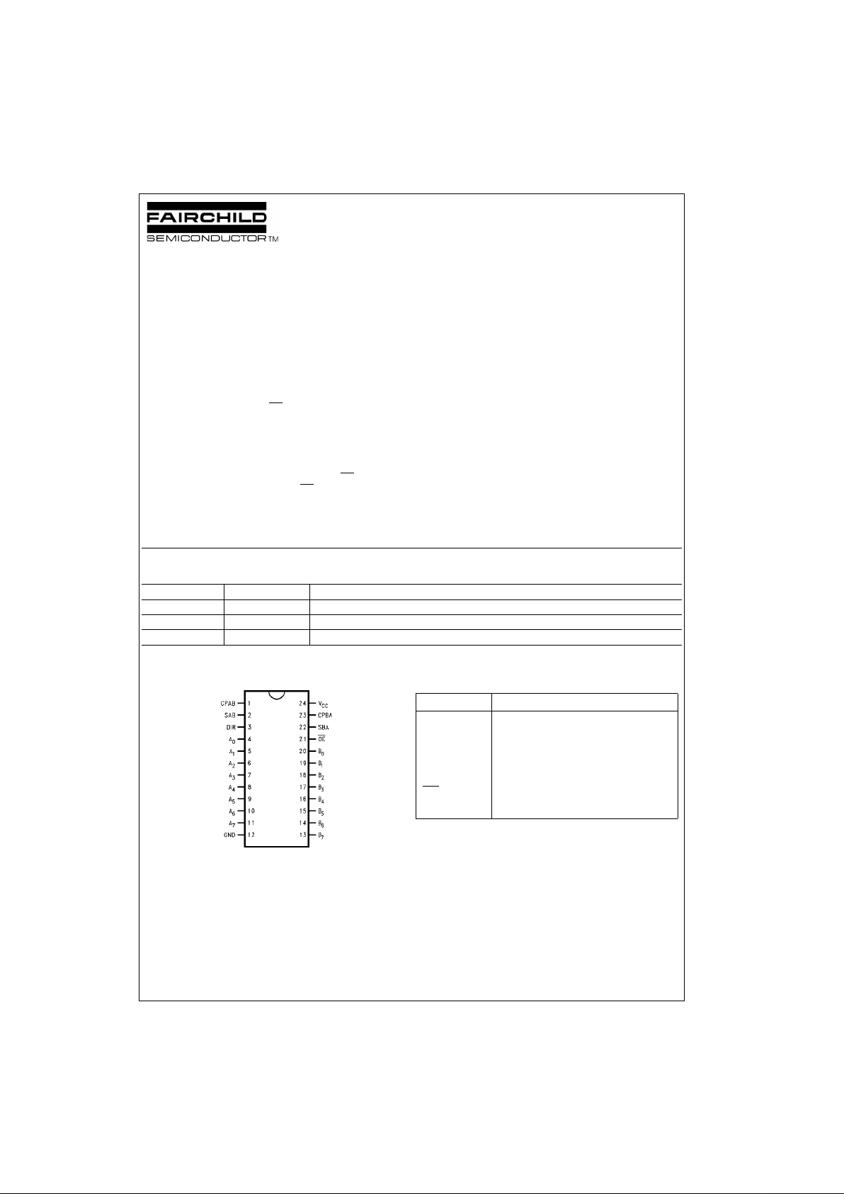
Connection Diagram Pin Descriptions
Order Number Package Number Package Description
74ABT646CSC M24B 24-Lead Small Outline Integrated Circuit (SOIC), JEDEC MS-153, 4.4mm Wide
74ABT646CMSA MSA24 24-Lead Shrink Small Outline Package (SSOP), EIAJ TYPE II, 5.3mm Wide
74ABT646CMTC MTC24 24-Lead Thin Shrink Small Outline Package (TSSOP), JEDEC MO-153, 4.4mm Wide
Pin Names Description
A
0–A7
Data Register A Inputs/3-STATE Outputs
B
0–B7
Data Register B Inputs/3-STATE Outputs
CPAB, CPBA Clock Pulse Inputs
SAB, SBA Select Inputs
OE
Output Enable Input
DIR Direction Control Input
Page 2
www.fairchildsemi.com 2
74ABT646
Truth Table
H = HIGH Voltage Level
L = LOW Voltage Level
X = Immaterial
= LOW-to-HIGH Transition
Note 1: The data output functions may be enabled or dis abled by various signals at the OE
and DIR inputs. Data input functions are always enabled;
i.e., data at the bus pins will be stored on every LOW-to-HIGH transition of the appropriate clock inputs.
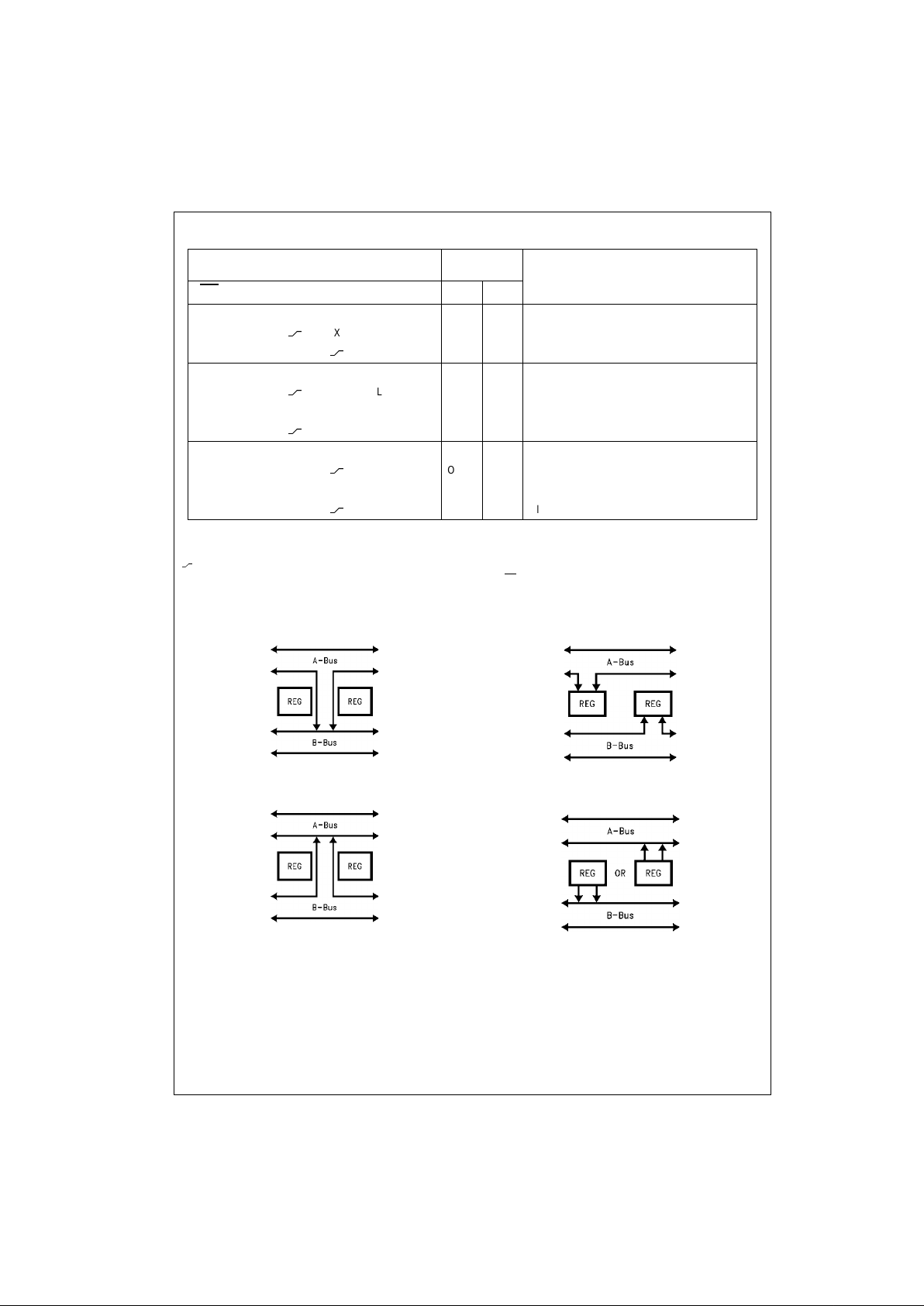
Real Time Transfer
A-Bus to B-Bus
FIGURE 1.
Real Time Transfer
B-Bus to A-Bus
FIGURE 2.
Storage from
Bus to Register
FIGURE 3.
Transfer from
Register to Bus
FIGURE 4.
Inputs Data I/O
(Note 1)
Function
OE
DIR CPAB CPBA SAB SBA A0–A7 B0–B
7
H X H or L H or L X X Isolation
H X
X X X Input Input Clock An Data into A Register
H X X
X X Clock Bn Data into B Register
L H X X L X A
n
to Bn—Real Time (Transparent Mode)
L H
X L X Input Output Clock An Data into A Register
L H H or L X H X A Register to B
n
(Stored Mode)
L H
X H X Clock An Data into A Register and Output to B
n
L L X X X L Bn to An—Real Time (Transparent Mode)
L L X
X L Output Input Clock Bn Data into B Register
L L X H or L X H B Register to A
n
(Stored Mode)
L L X
X H Clock Bn Data into B Register and Output to A
n
Page 3
3 www.fairchildsemi.com
74ABT646
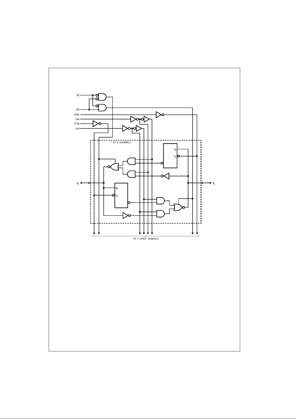
Logic Diagram
Please note that this diagram is provided only for the understanding of logic operations and should not be used to estimate propagation delays.
Page 4

www.fairchildsemi.com 4
74ABT646
Absolute Maximum Ratings(Note 2) Recommended Operating
Conditions
Note 2: Absolute maximum ratings are values beyond which the device
may be damaged or have its useful life impaired. Functional operation
under these conditi ons is not implied.
Note 3: Either voltage lim it or c urrent limit is sufficient to protect inputs.
DC Electrical Characteristics
Note 4: Guaranteed but not tested.
Note 5: For 8-bit toggling, I
CCD
< 1.4 mA/MHz.
Storage Temperature −65°C to +150°C
Ambient Temperature under Bias −55°C to +125°C
Junction Temperature under Bias −55°C to +150°C
V
CC
Pin Potential to Ground Pin −0.5V to +7.0V
Input Voltage (Note 3) −0.5V to +7.0V
Input Current (Note 3) −30 mA to +5.0 mA
Voltage Applied to Any Output
in the Disable or
Power-Off State −0.5V to +5.5V
in the HIGH State −0.5V to V
CC
Current Applied to Output
in LOW State (Max) twice the rated I
OL
(mA)
DC Latchup Source Current −500 mA
Over Voltage Latchup (I/O) 10V
Free Air Ambient Temperature −40°C to +85°C
Supply Voltage +4.5V to +5.5V
Minimum Input Edge Rate (∆V/∆t)
Data Input 50 mV/ns
Enable Inpu t 20 mV/n s
Clock Input 100 mV/ns
Symbol Parameter Min Typ Max U nits
V
CC
Conditions
V
IH
Input HIGH Voltage 2.0 V Recognized HIGH Signal
V
IL
Input LOW Voltage 0.8 V Recognized LOW Signal
V
CD
Input Clamp Diode Voltage −1.2 V Min IIN = −18 mA (Non I/O Pins)
V
OH
Output HIGH Voltage 2.5 IOH = −3 mA, (An, Bn)
2.0 IOH = −32 mA, (An, Bn)
V
OL
Output LOW Voltage 0.55 IOL = 64 mA, (An, Bn)
V
ID
Input Leakage Test 4.75 V 0.0 IID = 1.9 µA, (Non-I/O Pins)
All Other Pins Grounded
I
IH
Input HIGH Current 1
µA Max
VIN = 2.7V (Non-I/O Pins) (Note 4)
1 V
IN
= VCC (Non-I/O Pins)
I
BVI
Input HIGH Current
7 µA Max V
IN
= 7.0V (Non-I/O Pins)
Breakdown Test
I
BVIT
Input HIGH Current
100 µA Max VIN = 5.5V (An, Bn)
Breakdown Test (I/O)
I
IL
Input LOW Current −1
µA Max
VIN = 0.5V (Non-I/O Pins) (Note 4)
−1 V
IN
= 0.0V (Non-I/O Pins)
IIH + I
OZH
Output Leakage Current 10 µA 0V–5.5V
V
OUT
= 2.7V (An, Bn); OE = 2.0V
IIL + I
OZL
Output Leakage Current −10 µA 0V–5.5V
V
OUT
= 0.5V (An, Bn); OE = 2.0V
I
OS
Output Short-Circuit Current −100 −275 mA Max V
OUT
= 0V (An, Bn)
I
CEX
Output HIGH Leakage Current 50 µA Max V
OUT
= VCC (An, Bn)
I
ZZ
Bus Drainage Test 100 µA 0.0V V
OUT
= 5.5V (An, Bn);
All Others GND
I
CCH
Power Supply Current 250 µA Max All Outputs HIGH
I
CCL
Power Supply Current 30 mA Max All Outputs LOW
I
CCZ
Power Supply Current 50 µA Max Outputs 3-STATE; All Others GND
I
CCT
Additional ICC/Input 2.5 mA Max VI = VCC − 2.1V
All Other Outputs at VCC or GND
I
CCD
Dynamic I
CC
No Load Outputs OPEN
(Note 4)
0.18 mA/MHz Max
OE and DIR = GND,
Non-I/O = GND or VCC (Note 5)
One Bit toggling, 50% duty cycle
Page 5

5 www.fairchildsemi.com
74ABT646
DC Electrical Characteristics
Note 6: Max number of outputs defined as (n). n − 1 data inputs are driven 0V to 3V. One output at LOW. Guaranteed, but not tested.
Note 7: Max number of outputs defined as (n). n − 1 data inputs are driven 0V to 3V. One output HI GH . Guaranteed, but not tes t ed.
Note 8: Max number of data inputs (n) s witc hing. n − 1 inputs switching 0V to 3V. Input-under-test switching: 3V to threshold (V
ILD
), 0V to threshold (V
IHD
).
Guaranteed, but not tested.
AC Electrical Characteristics
(SOIC and SSOP package)
AC Operating Requirements
Symbol Parameter Min Typ Max Units
V
CC
Conditions
CL = 50 pF, RL = 500Ω
V
OLP
Quiet Output Maximum Dynamic V
OL
0.6 0.8 V 5.0 TA = 25°C (Note 6)
V
OLV
Quiet Output Minimum Dynamic V
OL
−1.2 −0.9 V 5.0 TA = 25°C (Note 6)
V
OHV
Minimum HIGH Level Dynamic Output Voltage 2.5 3.0 V 5.0 TA = 25° (Note 7)
V
IHD
Minimum HIGH Level Dynamic Input Voltage 2.2 1.8 V 5.0 TA = 25°C (Note 8)
V
ILD
Maximum LOW Level Dynamic Input Voltage 0.8 0.5 V 5.0 TA = 25°C (Note 8)
Symbol Parameter
TA = +25°C T
A
= −55°C to +125°C TA = −40°C to +85°C
Units
VCC = +5.0V VCC = 4.5V–5.5V VCC = 4.5V–5.5V
CL = 50 pF CL = 50 pF CL = 50 pF
Min Typ Max Min Max Min Max
f
MAX
Maximum Clock Frequency 200 200 200 MHz
t
PLH
Propagation Delay 1.7 3.0 5.6 2.2 8.8 1.7 5.6
ns
t
PHL
Clock to Bus 1.7 3.4 5.6 1.7 8.8 1.7 5.6
t
PLH
Propagation Delay 1.5 2.6 4.8 1.5 7.9 1.5 4.8
ns
t
PHL
Bus to Bus 1.5 3.0 4.8 1.5 7.9 1.5 4.8
t
PLH
Propagation Delay 1.5 3.0 5.9 1.5 8.1 1.5 5.9
ns
t
PHL
SBA or SAB to An to B
n
1.5 3.4 5.9 1.5 8.9 1.5 5.9
t
PZH
Enable Time 1.5 3.2 6.3 1.0 7.3 1.5 6.3
ns
t
PZL
OE to Anor B
n
1.5 3.5 6.3 1.9 8.8 1.5 6.3
t
PHZ
Disable Time 1.5 3.7 6.0 1.5 9.3 1.5 6.0
ns
t
PLZ
OE to Anor B
n
1.5 3.2 6.0 1.5 9.3 1.5 6.0
t
PZH
Enable Time 1.5 3.4 6.3 1.0 7.7 1.5 6.3
ns
t
PZL
DIR to An or B
n
1.5 3.7 6.3 2.2 9.5 1.5 6.3
t
PHZ
Disable Time 1.5 3.8 6.0 1.5 8.7 1.5 6.0
ns
t
PLZ
DIR to An or B
n
1.5 3.2 6.0 1.5 9.2 1.5 6.0
Symbol Parameter
TA = +25°C TA = −55°C to +125°C TA = −40°C to +85°C
Units
VCC = +5.0V VCC = 4.5V–5.5V VCC = 4.5V–5.5V
CL = 50 pF CL = 50 pF CL = 50 pF
Min Max Min Max Min Max
tS(H) Setup Time, HIGH
1.5 1.5 3.0 1.5 ns
tS(L) or LOW Bus to Clock
tH(H) Hold Time, HIGH
1.0 1.0 1.0 1.0 ns
tH(L) or LOW Bus to Clock
tW(H) Pulse Width,
3.0 3.0 4.0 3.0 ns
tW(L) HIGH or LOW
Page 6

www.fairchildsemi.com 6
74ABT646
Extended AC Electrical Characteristics
(SOIC Package)
Note 9: This specification is gu aranteed but not tested . The limits apply to propagation delays for all paths described switching in ph ase
(i.e., all LOW-to-HIGH, HIGH-to-LOW, etc.).
Note 10: This specificatio n is guaranteed but not tested. Th e limits represent propagation d elay with 25 0 pF load capacitors i n place of the 50 pF load capacitors in the standard AC load. This specifica ti on pertains to single output switching only.
Note 11: This specification is guaranteed but not tested. The limits represent propagation delays for all paths described switching in phase
(i.e., all LOW-to-HIGH, HIGH-to-LOW, etc.) with 250 pF load capacitors in place of the 50 pF load capacitors in the standard AC load.
Note 12: The 3-STATE delays are dominated by the RC n et work (500Ω, 250 pF) on the output and has been excluded from the datasheet.
Skew
(SOIC Package)
Note 13: This specification is guaranteed but not teste d. Th e limits apply to propagat ion delays for all paths des c ribed switching in phase
(i.e., all LOW-to-HIGH, HIGH-to-LOW, etc.).
Note 14: This specification is guaranteed b ut not tested. The limits repre sent propag ation delays wit h 250 pF load capacitors in place of the 50 pF load
capacitors in the standard AC load.
Note 15: Skew is defined as the absolu te valu e of the differe nce bet ween the actu al propag ation de lays for a ny two s eparat e outpu ts of the s ame devic e.
The specificatio n appli es to any o utpu ts swit chi ng HIG H-t o-LO W (t
OSHL
), LOW-to-HIGH (t
OSLH
), or any combinatio n sw itchin g LO W-to-H IGH a nd /or HI GH-
to-LOW (t
OST
). This specification is guaranteed but not tested.
Note 16: This desc ribes the differe nce be tween th e d elay of the LOW-t o-H IGH an d th e H IGH-t o-LO W t rans itio n on the sam e p in. I t is mea sure d across all
the outputs (drivers ) on the same chip, the wors t (largest delta) number is t he guaranteed specification. This specification is guaranteed but not tested.
Note 17: Propagation dela y variation for a given se t of c onditions (i.e., temperature and V
CC
) from device to device. This specification is guaranteed but not
tested.
Capacitance
Note 18: C
I/O
is measured at frequency, f = 1 MHz, per MIL-STD-883, Method 3012.
Symbol Parameter
TA = −40°C to +85°C TA = −40°C to +85°C TA = −40°C to +85°C
Units
VCC = 4.5V–5.5V VCC = 4.5V–5.5V VCC = 4.5V–5.5V
CL = 50 pF CL = 250 pF CL = 250 pF
8 Outputs Switching 1 Output Switching 8 Outputs Switching
(Note 9) (Note 10) (Note 11)
Min Max Min Max Min Max
t
PLH
Propagation Delay 1.5 5.5 2.0 7.5 2.5 10.0
ns
t
PHL
Clock to Bus 1.5 5.5 2.0 7.5 2.5 10.0
t
PLH
Propagation Delay 1.5 6.0 2.0 7.0 2.5 9.5
ns
t
PHL
Bus to Bus 1.5 6.0 2.0 7.0 2.5 9.5
t
PLH
Propagation Delay 1.5 6.0 2.0 7.5 2.5 10.0 ns
t
PHL
SBA or SAB to An or B
n
1.5 6.0 2.0 7.5 2.5 10.0
t
PZH
Output Enable Time 1.5 6.0 2.0 8.0 2.5 10.5
ns
t
PZL
OEn or DIR to An or B
n
1.5 6.0 2.0 8.0 2.5 10.5
t
PHZ
Output Disable Time 1.5 6.0
(Note 12) (Note 12) ns
t
PLZ
OEn or DIR to An or B
n
1.5 6.0
Symbol Parameter
T
A
= −40°C to +85°C TA = −40°C to +85°C
Units
VCC = 4.5V–5.5V VCC = 4.5V–5.5V
C
L
= 50 pF CL = 250 pF
8 Outputs Switching 8 Outputs Switching
(Note 13) (Note 14)
Max Max
t
OSHL
(Note 15) Pin to Pin Skew, HL Transitions 1.3 2.5 ns
t
OSLH
(Note 15) Pin to Pin Skew, LH Transitions 1.0 2.0 ns
tPS (Note 16) Duty Cycle, LH–HL Skew 2.0 4.0 ns
t
OST
(Note 15) Pin to Pin Skew, LH/HL Transitions 2.0 4.0 ns
t
PV
(Note 17) Device to Device Skew, LH/HL Transitions 2.5 4.5 ns
Symbol Parameter Typ Units
Conditions
TA = 25°C
C
IN
Input Capacitance 5 pF VCC = 0V (non I/O pins)
C
I/O
(Note 18) Output Capacitance 11 pF VCC = 5.0V (An, Bn)
Page 7

7 www.fairchildsemi.com
74ABT646
AC Loading
*Includes jig and probe capacitance
FIGURE 5. Standard AC Test Load
FIGURE 6. Test Input Signal Levels
Input Pulse Requirements
FIGURE 7. Test Input Signal Requirements
AC Waveforms
FIGURE 8. Propagation Delay Waveforms for Inverting
and Non-Inve rting Functions
FIGURE 9. Propagation Delay,
Pulse Width Waveforms
FIGURE 10. 3-STATE Output HIGH
and LOW Enable and Disable Times
FIGURE 11. Setup Time, Hold Time
and Recovery Time Waveforms
Amplitude Rep. Rate t
W
t
r
t
f
3.0V 1 MHz 500 ns 2.5 ns 2.5 ns
Page 8

www.fairchildsemi.com 8
74ABT646
Physical Dimensions inches (millimeters) unless otherwise noted
24-Lead Small Outline Integrated Circuit (SOIC), JEDEC MS-013, 0.300” Wide Body
Package Number M24B
24-Lead Shrink Small Outline Package (SSOP), EIAJ TYPE II, 5.3mm Wide
Package Number MSA24
Page 9

9 www.fairchildsemi.com
74ABT646 Octal Transceivers and Registers with 3-STATE Outputs
Physical Dimensions inches (millimeters) unless otherwise noted (Continued)
24-Lead Thin Shrink Sm all Ou tline Pa ck age (TS SO P), JE DE C MO-153, 4.4mm Wide
Package Number MTC24
Fairchild does not assume any responsibility for use of any circuitry described , no circuit patent licenses are implied and
Fairchild reserves the right at any time without notice to change said circuitry and specifications.
LIFE SUPPORT POLICY
FAIRCHILD’S PRODUCTS ARE NOT AUTHORIZED FOR USE AS CRITICAL COMPONENTS IN LIFE SUPPORT
DEVICES OR SYSTEMS WITHOUT THE EXPRESS WRITTEN APPROVAL OF THE PRESIDENT OF FAIRCHILD
SEMICONDUCTOR CORPORATION. As used herein:
1. Life support devices or systems are dev ic es or syste ms
which, (a) are intended for surgical implant into the
body, or (b) support or sustain life, and (c) whose failure
to perform when properly used in accordance with
instructions for use provide d in the labe l ing, can be re asonably expected to result in a significant injury to the
user.
2. A critical compo nent in any com ponen t of a life s upp ort
device or system whose failure to perform can be reasonably expected to cause the failure of the l ife support
device or system, or to affect its safety or effectiveness.
www.fairchildsemi.com
 Loading...