

Datasheet 74ABT543CSPC, 74ABT543CSCX, 74ABT543CSC, 74ABT543CMTCX, 74ABT543CMTC Datasheet (Fairchild Semiconductor)
...Page 1
November 1992
Revised January 1999
74ABT543 Octal Registered Transceiver with 3-STATE Outputs
© 1999 Fairchild Semiconductor Corporation DS011508.prf www.fairchildsemi.com
74ABT543
Octal Registered Transceiver with 3-STATE Outputs
General Description
The ABT543 octal transceiver conta ins two sets of D-type
latches for temporary storage of data flowing in either
direction. Separate Latch Enable and Output Enabl e inputs
are provided for each register to permit indep endent control of inputting and outputt ing in either direction of data
flow.
Features
■ Back-to-back registers for storage
■ Bidirectional data path
■ A and B outputs have current sourcing capability of 32
mA and current sinking capability of 64 mA
■ Separate controls for data flow in each direction
■ Guaranteed output skew
■ Guaranteed multiple output switching specifications
■ Output switching specified for both 5 0 pF and 250 pF
loads
■ Guaranteed simultaneous switching noise level and
dynamic threshold performance
■ Guaranteed latchup protection
■ High impedance glitch free bus loading during entire
power up and power down cycle
■ Nondestructive hot insertion capability
Ordering Code:
Device also available in Tape and Reel. Specify by appendin g s uf f ix let t er “X” to the ordering co de.
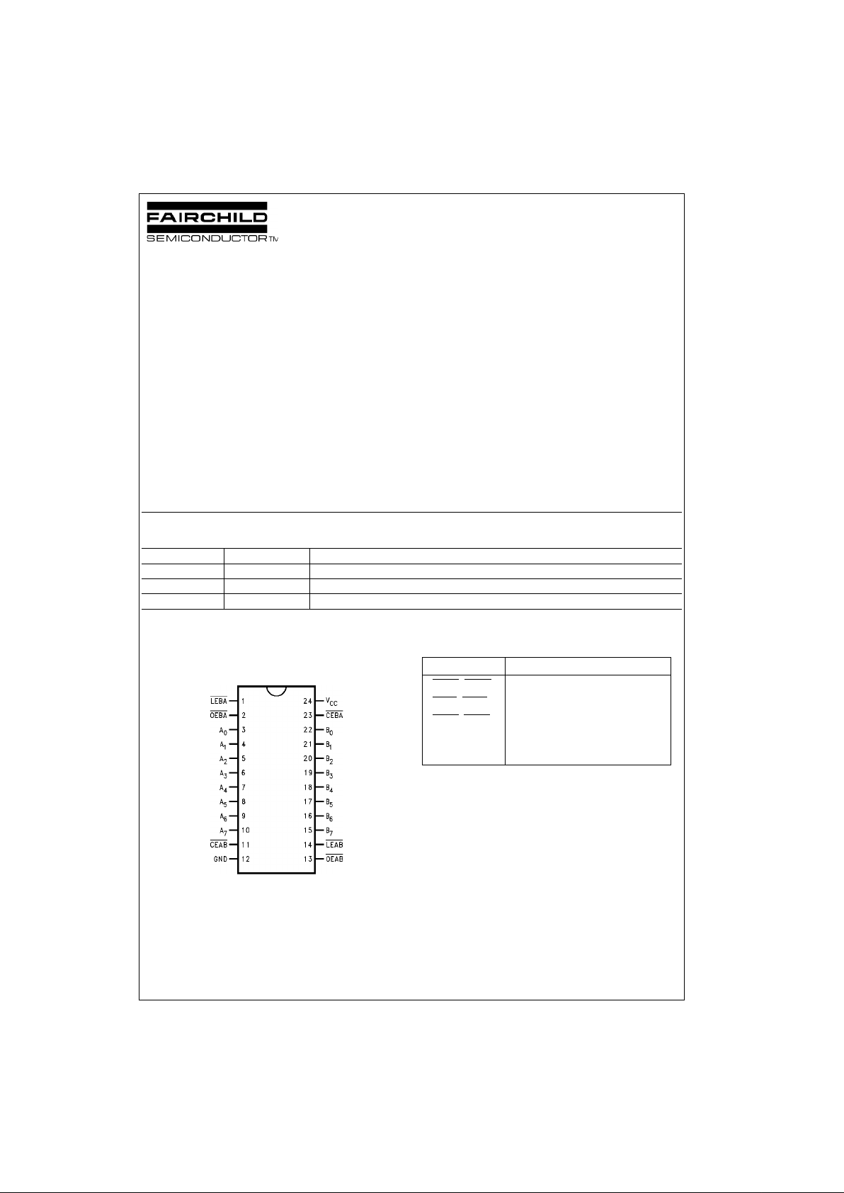
Connection Diagram
Pin Assignment for
SOIC, SSOP and TSSOP
Pin Descriptions
Order Number Package Number Package Description
74ABT543CSC M24B 24-Lead Small Outline Integrated Circuit (SOIC), JEDEC MS-013, 0.300” Wide Body
74ABT543CMSA MSA24 24-Lead Shrink Small Outline Package (SSOP), EIAJ TYPE II, 5.3mm Wide
74ABT543CMTC MTC24 24-Lead Thin Shrink Small Outline Package (TSSOP), JEDEC MO-153, 4.4mm Wide
Pin Names Description
OEAB
, OEBA Output Enable Inputs
LEAB
, LEBA Latch Enable Inputs
CEAB
, CEBA Chip Enable Inputs
A
0–A7
Side A Inputs or 3-STATE Outputs
B
0–B7
Side B Inputs or 3-STATE Outputs
Page 2
www.fairchildsemi.com 2
74ABT543
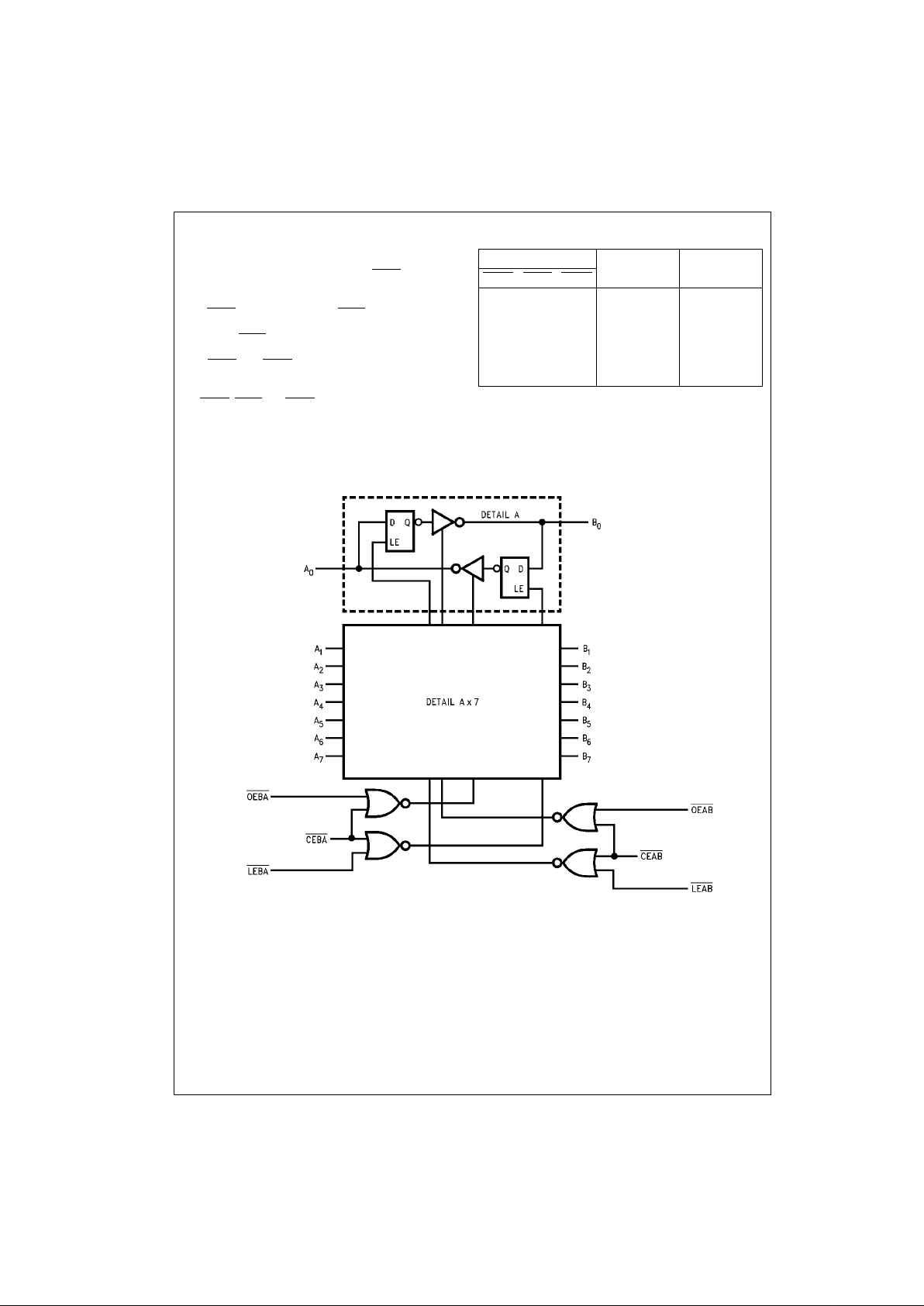
Functional Description
The ABT543 contains two sets of D-type latches, with separate input and output co ntr ols for each. For data flow fro m
A to B, for example, the A to B Enable (CEAB
) input must
be low in order to enter data from the A Port or take da ta
from the B Port as i ndicated in the Da ta I/O Contr ol Table.
With CEAB
low, a low signal on (LEAB) input makes the A
to B latches transparent; a subse quent low to high transition of the LEAB
line puts the A latches in the storage
mode and their outputs no longer change with the A inputs.
With CEAB
and OEAB both low, the B output buffers are
active and reflect the data present on the output of the A
latches. Control of data flow from B to A is similar, but using
the CEBA
, LEBA and OEBA.
Data I/O Control Table
H = HIGH Voltage Level
L = LOW Voltage Level
X = Immaterial
Logic Diagram
Inputs Latch Status Output Buffers
CEAB
LEAB OEAB
H X X Latched HIGH Z
X H X Latched —
L L X Transparent —
X X H — HIGH Z
L X L — Driving
Page 3
3 www.fairchildsemi.com
74ABT543
Absolute Maximum Ratings(Note 1)
Recommended Operating
Conditions
Note 1: Absolute maximum ratings are values beyond which the device
may be damaged or have its useful life impaired. Functional operation
under these condit ions is not implied.
Note 2: Either voltage limit or current limi t is s uf f ic ient to protect inputs.
DC Electrical Characteristics
Note 3: Guaranteed but not tested.
Note 4: For 8-bit toggling. I
CCD
< 1.4 mA/MHz.
Note 5: Guaranteed, but not tested.
Storage Temperature −65°C to +150°C
Ambient Temperature under Bias −55°C to +125°C
Junction Tem perature under Bias −55°C to +150°C
V
CC
Pin Potential to
Ground Pin −0.5V to +7.0V
Input Voltage (Note 2) −0.5V to +7.0V
Input Current (Note 2) −30 mA to +5.0 mA
Voltage Applied to Any Output
in the Disable or Power-Off State −0.5V to +5.5V
in the HIGH State −0.5V to V
CC
Current Applied to Output
in LOW State (Max)
twice the rated I
OL
(mA)
DC Latchup Source Current −500 mA
Over Voltage Latchup (I/O) 10V
Free Air Ambient Temperature −40°C to +85°C
Supply Voltage +4.5V to +5.5V
Minimum Input Edge Rate (∆V/∆t)
Data Input 50 mV/ns
Enable Input 20 mV/ns
Clock Input 100 mV/ns
Symbol Parameter Min Typ Max Units
V
CC
Conditions
V
IH
Input HIGH Voltage 2.0 V Recognized HIGH Signal
V
IL
Input LOW Voltage 0.8 V Recognized LOW Signal
V
CD
Input Clamp Diode Voltage −1.2 V IIN = −18 mA (Non I/O Pins)
V
OH
Output HIGH Voltage 2.5 IOH = −3 mA, (An, Bn)
2.0 IOH = −32 mA, (An, Bn)
V
OL
Output LOW Voltage 0.55 V Min IOL = 64 mA, (An, Bn)
V
ID
Input Leakage Test 4.75 V 0.0 IID = 1.9 µA, (Non-I/O Pins)
All Other Pins Grounded
I
IH
Input HIGH Current 1 µAMaxVIN = 2.7V (Non-I/O Pins) (Note 3)
1V
IN
= VCC (Non-I/O Pins)
I
BVI
Input HIGH Current Breakdown Test 7 µAMaxVIN = 7.0V (Non-I/O Pins)
I
BVIT
Input HIGH Current 100 µAMaxVIN = 5.5V (An, Bn)
Breakdown Test (I/O)
I
IL
Input LOW Current −1 µAMaxVIN = 0.5V (Non-I/O Pins) (Note 3)
−1V
IN
= 0.0V (Non-I/O Pins)
IIH+ I
OZH
Output Leakage Current 10 µA 0V–5.5V V
OUT
= 2.7V (An, Bn);
OEAB or CEAB = 2V
IIL + I
OZL
Output Leakage Current −10 µA 0V–5.5V V
OUT
= 0.5V (An, Bn);
OEAB or CEAB = 2V
I
OS
Output Short-Circuit Current −100 −275 mA Max V
OUT
= 0V (An, Bn)
I
CEX
Output HIGH Leakage Current 50 µAMaxV
OUT
= VCC (An, Bn)
I
ZZ
Bus Drainage Test 100 µA0.0VV
OUT
= 5.5V (An, Bn);
All Others GND
I
CCLH
Power Supply Current 50 µA Max All Outputs HIGH
I
CCL
Power Supply Current 30 mA Max All Outputs LOW
I
CCZ
Power Supply Current 50 µA Max Outputs 3-STATE
All Others at VCC or GND
I
CCT
Additional ICC/Input 2.5 mA Max VI = VCC − 2.1V
All Others at VCC or GND
I
CCD
Dynamic I
CC
No Load
Outputs Open, CEAB
(Note 5) 0.18 mA/MHz Max
and OEAB = GND, CEBA = VCC, One Bit Toggling,
50% Duty Cycle, (Note 4)
Page 4

www.fairchildsemi.com 4
74ABT543
DC Electrical Characteristics
(SOIC Package)
Note 6: Max number of outputs defined as (n) . n − 1 dat a inputs are driven 0V to 3V. One output at LOW. Guaranteed, but not te s te d.
Note 7: Max number of outputs defined as (n) . n−1 data inputs are dr iven 0V t o 3V. One output HIGH. Guaranteed, but not teste d.
Note 8: Max number of data i npu ts (n) swit chin g. n − 1 inpu ts switc hing 0 V to 3 V. Input-under-test switc hing: 3V t o thr esho ld (V
ILD
), 0V to threshold (V
IHD
).
Guaranteed, but not tes t ed.
AC Electrical Charac teristics
(SOIC and SSOP Packages)
AC Operating Requirements
(SOIC and SSOP Packages)
Conditions
Symbol Parameter Min Typ Max Units
V
CC
CL = 50 pF,
RL = 500Ω
V
OLP
Quiet Output Maximum Dynamic V
OL
0.7 1.0 V 5.0 TA = 25°C (Note 6)
V
OLV
Quiet Output Minimum Dynamic V
OL
−1.2 −0.8 V 5.0 TA = 25°C (Note 6)
V
OHV
Minimum HIGH Level Dynamic Output Voltage 2.5 3.0 V 5.0 TA = 25°C (Note 7)
V
IHD
Minimum HIGH Level Dynamic Input Voltage 2.0 1.7 V 5.0 TA = 25°C (Note 8)
V
ILD
Maximum LOW Level Dynamic Input Voltage 0.7 0.9 V 5.0 TA = 25°C (Note 8)
Symbol Parameter
TA = +25°CT
A
= −40°C to +85°C
Units
VCC = +5.0V VCC = 4.5V–5.5V
CL = 50 pF CL = 50 pF
Min Typ Max Min Max
t
PLH
Propagation Delay 1.5 3.1 4.8 1.5 4.8 ns
t
PHL
An to Bn or Bn to A
n
1.5 4.8 1.5 4.8
t
PLH
Propagation Delay
t
PHL
LEAB to Bn, LEBA to A
n
1.6
3.4
5.3 1.6 5.3
ns
OEBA or OEAB to An or B
n
1.6 5.3 1.6 5.3
t
PZH
Enable Time
t
PZL
LEAB to Bn, LEBA to A
n
1.5
3.6
5.8 1.5 5.8
ns
OEBA or OEAB to An or B
n
1.5 5.8 1.5 5.8
t
PHZ
Disable Time 2.0 4.0 6.5 2.0 6.5 ns
t
PLZ
CEBA or CEAB to An or B
n
2.0 6.5 2.0 6.5
Symbol Parameter
TA = +25°CT
A
= −40°C to +85°C
Units
VCC = +5.0V VCC = 4.5V–5.5V
CL = 50 pF CL = 50 pF
MinMaxMinMax
tS(H) Setup Time, HIGH or LOW 1.5 1.5 ns
tS(L)
An or Bn to LEBA or LEAB
1.5 1.5
tH(H) Hold Time, HIGH or LOW 1.0 1.0 ns
tH(L)
An or Bn to LEBA or LEAB
1.0 1.0
tS(H) Setup Time, HIGH or LOW 1.5 1.5 ns
tS(L)
An or Bn to CEAB or CEBA
1.5 1.5
tH(H) Hold Time, HIGH or LOW 1.3 1.3 ns
tH(L)
An or Bn to CEAB or CEBA
1.3 1.3
tW(L) Pulse Width, LOW 3.0 3.0 ns
Page 5

5 www.fairchildsemi.com
74ABT543
Extended AC Electri cal Characteristics
(SOIC Package)
Note 9: This specification is guarantee d but not tested . The limits ap ply to propaga tion delays for all paths de scribe d switching in phas e (i.e., all LOW-toHIGH, HIGH-to-LOW, et c.) .
Note 10: This specification is guaranteed but not tested. The limi ts represent propagation delay with 250pF load capacito rs in plac e of the 50 pF lo ad capacitors in the standard AC load . Th is sp ec if ic ation pertains to sin gle output switching only.
Note 11: This specific at ion is guaranteed but not tested. The lim its represent propagation delays for all paths described switching in phase (i.e., all LOW-toHIGH, HIGH-to-LOW, etc.) with 250 pF load capacitors in place of th e 50 pF load capacitor s in th e s ta ndard AC load.
Note 12: The 3-STATE delay times are dominated by the RC network (500Ω, 250 pF) on the output and has been excluded fr om t he datasheet
Skew
(SOIC Package)
Note 13: This specific ation is gua ranteed but not tested . The limit s apply to propagat ion delays for all pa ths descr ibed switching in phase (i.e., all LOW-toHIGH, HIGH-to-LOW, et c.) .
Note 14: This spec ification is gua ranteed but not t ested. The lim its represent p ropagation d elays with 250 pF load cap acitors in place of the 50 pF load
capacitors in the standard AC load.
Note 15: Skew is defined a s the ab solute value of t he dif ference bet ween the actu al propa gation delays for any two sepa rate ou tputs o f the same device.
The specification a pplies to a ny outpu ts switching H IGH-to -LOW (t
OSHL
), LOW-to-HIGH (t
OSLH
), or any combination switching LOW-to-HIGH and/or HIGH-
to-LOW (t
OST
). This specification is guaranteed but not tested.
Note 16: This descri bes the dif ference betwee n the delay of th e LOW-to-HIGH an d the HIGH -to-LOW trans ition on the same p in. It is measu red ac ross al l
the outputs (drivers) on th e s am e chip, the worst (largest delt a) number is the guarante ed specification. This s pecification is guarante ed but not tested.
Note 17: Propagation delay variation for a given s et of conditions ( i.e., t em perature and V
CC
) from device to device. T his specification is guaranteed but not
tested.
Symbol Parameter
TA = −40°C to +85°CTA = −40°C to +85°CTA = −40°C to +85°C
Units
VCC = 4.5V–5.5V VCC = 4.5V–5.5V VCC = 4.5V–5.5V
CL = 50 pF CL = 250 pF CL = 250 pF
8 Outputs Switching 1 Output Switching 8 Outputs Switching
(Note 9) (Note 10) (Note 11)
Min Typ Max Min Max Min Max
f
TOGGLE
Max Toggle Frequency 100 MHz
t
PLH
Propagation Delay 1.5 6.2 2.0 7.5 2.5 10.0 ns
t
PHL
An to Bn or Bn to A
n
1.5 6.2 2.0 7.5 2.5 10.0
t
PLH
Propagation Delay 1.5 6.5 2.0 8.0 2.5 10.5 ns
t
PHL
LEAB to Bn, LEBA to A
n
1.5 6.5 2.0 8.0 2.5 10.5
t
PZH
Output Enable Time
t
PZL
OEBA or OEAB to An or B
n
1.5 7.5 2.0 8.5 2.5 11.0 ns
CEBA or CEAB to An or B
n
1.5 7.5 2.0 8.5 2.5 11.0
t
PHZ
Output Disable Time
t
PLZ
OEBA or OEAB to An or B
n
1.5 8.5
(Note 12) (Note 12) ns
CEBA or CEAB to An or B
n
1.5 8.5
Symbol Parameter
TA = −40°C to +85°CTA = −40°C to +85°C
Units
VCC = 4.5V–5.5V VCC = 4.5V–5.5V
CL = 50 pF CL = 250 pF
8 Outputs Switching 8 Outputs Switching
(Note 13) (Note 14)
Max Max
t
OSHL
Pin to Pin Skew 1.0 2.0 ns
(Note 15) HL Transitions
t
OSLH
Pin to Pin Skew 1.3 2.0 ns
(Note 15) LH Transitions
t
PS
Duty Cycle 2.0 4.0 ns
(Note 16) LH–HL Skew
t
OST
Pin to Pin Skew 2.0 4.0 ns
(Note 15) LH/HL Transitions
t
PV
Device to Device Skew 2.5 4.5 ns
(Note 17) LH/HL Transitions
Page 6

www.fairchildsemi.com 6
74ABT543
Capacitance
Note 18: C
I/O
is measured at frequency, f = 1 MHz, PER MLT-STD-883B, METHOD 3012.
AC Loading
*Includes jig and pr obe capacitance
FIGURE 1. Standard AC Test Load
FIGURE 2. V
M
= 1.5V
Input Pulse Requirements
FIGURE 3. Test Input Signal Requirements
AC Waveforms
FIGURE 4. Propagation Delay Waveforms for Inverting
and Non-Inverting Functions
FIGURE 5. Propagation Delay,
Pulse Width Waveforms
FIGURE 6. 3-STATE Output HIGH
and LOW Enable and Disable Times
FIGURE 7. Setup Time, Hold Time
and Recovery Time Waveforms
Symbol Parameter Typ Units
Conditions: TA = 25°C
C
IN
Input Capacitance 5.0 pF VCC = 0V (non I/O pins)
C
I/O
(Note 18) Output Capacitance 11.0 pF VCC = 5.0V (An, Bn)
Amplitude Rep. Rate t
W
t
r
t
f
3V 1 MHz 500 ns 2.5 ns 2.5 ns
Page 7

7 www.fairchildsemi.com
74ABT543
Physical Dimensions inches (millimeters) unless otherwise noted
24-Lead Small Outline Integrated Circuit (SOIC), JEDEC MS-013, 0.300” Wide Body
Package Number M24B
24-Lead Shrink Small Outline Package (SSOP), EIAJ TYPE II, 5.3mm Wide
Package Number MSA24
Page 8

Fairchild does not assume any responsibility for use of any circuitry described, no circuit patent licenses are implied and Fairchild reserves the right at any time without notice to change said circuitry and specifications.
74ABT543 Octal Registered Transceiver with 3-STATE Outputs
LIFE SUPPORT POLICY
FAIRCHILD’S PRODUCTS ARE NOT AUTHORIZED FOR USE AS CRITICAL COMPONENTS IN LIFE SUPPORT
DEVICES OR SYSTEMS WITHOUT THE EXPRESS WRITTEN APPROVAL OF THE PRESIDENT OF FAIRCHILD
SEMICONDUCTOR CORPORATION. As used herein:
1. Life support devices or systems are devices or syste ms
which, (a) are intended for surgical implant into the
body, or (b) support or sustain life, and (c) whose failure
to perform when properly used in accordance with
instructions for use provided in the labeling, can be reasonably expected to result in a significant injury to the
user.
2. A critical component in any compon ent of a life suppo r t
device or system whose failure to perform can be reasonably expected to cause the failure of the life suppor t
device or system, or to affect its safety or effectiveness.
www.fairchildsemi.com
Physical Dimensions inches (millimeters) unless otherwise noted (Continued)
24-Lead Thin Shrink Small Outline Package (TSSOP), JEDEC MO-153, 4.4mm Wide
Package Number MTC24
 Loading...