

Datasheet 74ABT373CMTCX, 74ABT373CMTC, 74ABT373CMSAX, 74ABT373CMSA, 74ABT373CSJX Datasheet (Fairchild Semiconductor)
...Page 1
© 1999 Fairchild Semiconductor Corporation DS011547 www.fairchildsemi.com
January 1993
Revised November 1999
74ABT373 Octal Transparent Latch with 3-STATE Outputs
74ABT373
Octal Transparent Latch with 3-STATE Outputs
General Description
The ABT373 consists of eight latches with 3-STATE outputs for bus organized system applications. The flip-f lops
appear transparent to the data w hen Latch En able (LE) i s
HIGH. When LE is LOW, the data that m eets the setup
times is latched. Data appears on the bus when the Output
Enable (OE
) is LOW. When OE is HIGH the bus output is in
the high impedance state.
Features
■ 3-STATE outputs for bus interfacing
■ Output sink capability of 64 mA, source capability of
32 mA
■ Guaranteed output skew
■ Guaranteed multiple output switching specifications
■ Output switching sp ecified for both 50 pF and 250 pF
loads
■ Guaranteed simultaneous switching, noise level and
dynamic threshold performan ce
■ Guarante ed latchup protection
■ High impedance glitch free bus loading during entire
power up and power down
■ Nondestructive hot insertion capability
Ordering Code:
Device also available in Tape and Reel. Specify by appending suffix letter “X” to the ordering code.
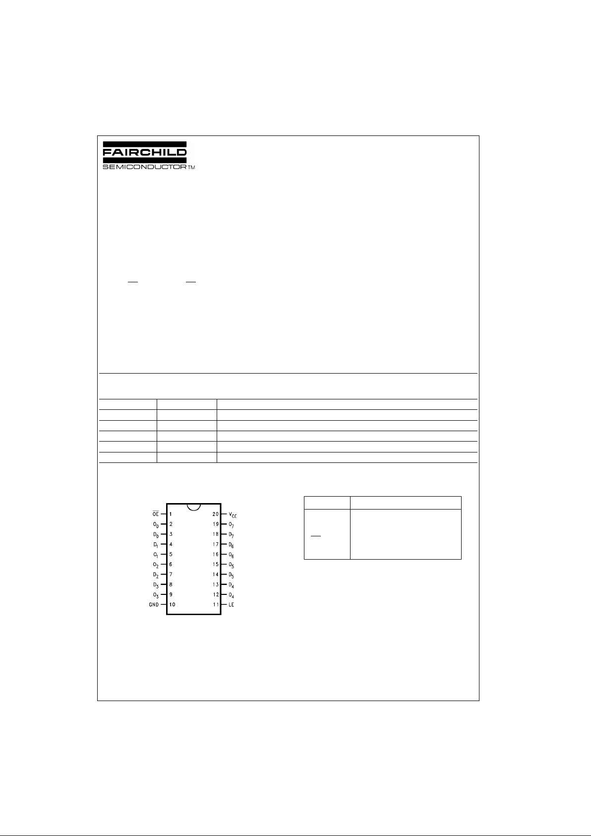
Connection Diagram Pin Descriptions
Order Number Package Number Package Description
74ABT373CSC M20B 20-Lead Small Outline Integrated Circuit (SOIC), JEDEC MS-013, 0.300” Wide Body
74ABT373CSJ M20D 20-Lead Small Outline Package (SOP), EIAJ TYPE II, 5.3mm Wide
74ABT373CMSA MSA20 20-Lead Shrink Small Outline Package (SSOP), EIAJ TYPE II, 5.3mm Wide
74ABT373CMTC MTC20 20-Lead Thin Shrink Small Outline Package (TSSOP), JEDEC MO-153, 4.4mm Wide
74ABT373CPC N20A 20-Lead Plastic Dual-In-Line Package (PDIP), JEDEC MS-001, 0.300” Wide
Pin Names Description
D
0–D7
Data Inputs
LE Latch Enable Input (Active HIGH)
OE
Output Enable Input (Active LOW)
O
0–O7
3-STATE Latch Outputs
Page 2
www.fairchildsemi.com 2
74ABT373
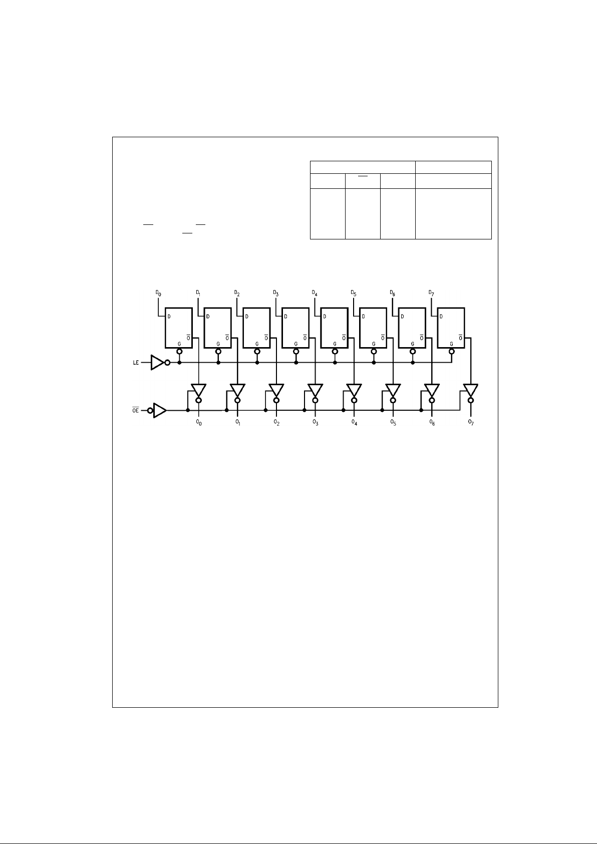
Functional Description
The ABT373 contains eig ht D-type latches with 3-STATE
output buffers. When the La tch Enab le ( LE) inpu t is HI GH,
data on the D
n
inputs enters the latches. In this conditio n
the latches are transparent, i.e., a latch output will change
state each time its D input ch anges. When LE is LOW, the
latches store the information that was present on th e D
inputs at setup time p recedin g the HIGH- to- LO W tra nsitio n
of LE. The 3-STATE buffers are controlled by th e Output
Enable (OE
) input. When OE is LOW, the buffers are in the
bi-state mode. When OE
is HIGH the buffers are in the high
impedance mode but this does not interfere with entering
new data into the latches.
Tr uth Table
H = HIGH Voltage Level
L = LOW Voltage Level
X = Immaterial
Z = HIGH Impedance State
Logic Diagram
Please note that this diagram is provided only for the understanding of logic operations and should not be used to estimate propagation dela ys.
Inputs Output
LE OE D
n
O
n
HLH H
HLL L
LLXO
n
(no change)
XHX Z
Page 3
3 www.fairchildsemi.com
74ABT373
Absolute Maximum Ratings(Note 1) Recommended Operating
Conditions
Note 1: Absolute maximum ratings are values beyond which the device
may be damaged or have its useful life impaired . Functional operation
under these conditions is not implied.
Note 2: Either voltage lim it or c urrent limit is sufficient to protect inputs.
DC Electrical Characteristics
Note 3: For 8 bits toggling, I
CCD
< 0.8 mA/MHz.
Note 4: Guaranteed, but not tested.
Storage Temperature −65°C to +150°C
Ambient Temperature under Bias −55°C to +125°C
Junction Temperature under Bias −55°C to +150°C
V
CC
Pin Potential to Ground Pin −0.5V to +7.0V
Input Voltage (Note 2) −0.5V to +7.0V
Input Current (Note 2) −30 mA to +5.0 mA
Voltage Applied to Any Output
in the Disabled or
Power-Off State −0.5V to +5.5V
in the HIGH State −0.5V to V
CC
Current Applied to Output
in LOW State (Max) twice the r ated I
OL
(mA)
DC Latchup Source Current:
OE
Pin −150 mA
(Across Comm Operating Range) Other Pins −500 mA
Over Voltage Latchu p (I/O) 10V
Free Air Ambient Temperature −40°C to +85°C
Supply Voltage +4.5V to +5.5
Minimum Input Edge Rate (∆V/∆t)
Data Input 50 mV/ns
Enable Input 20 mV/ns
Symbol Parameter Min Typ Max Units
V
CC
Conditions
V
IH
Input HIGH Voltage 2.0 V Recognized HIGH Signal
V
IL
Input LOW Voltage 0.8 V Recognized LOW Signal
V
CD
Input Clamp Diode Voltage −1.2 V Min IIN = −18 mA
V
OH
Output HIGH Voltage 2.5
VMin
IOH = −3 mA
2.0 IOH = −32 mA
V
OL
Output LOW Voltage 0.55 V Min IOL = 64 mA
I
IH
Input HIGH Current 1
µAMax
VIN = 2.7V (Note 4)
1V
IN
= V
CC
I
BVI
Input HIGH Current Breakdown Test 7 µAMaxVIN = 7.0V
I
IL
Input LOW Current −1
µAMax
VIN = 0.5V (Note 4)
−1V
IN
= 0.0V
V
ID
Input Leakage Test 4.75 V 0.0 IID = 1.9 µA
All Other Pins Grounded
I
OZH
Output Leakage Current 10 µA0 − 5.5V
V
OUT
= 2.7V; OE = 2.0V
I
OZL
Output Leakage Current −10 µA0 − 5.5V
V
OUT
= 0.5V; OE = 2.0V
I
OS
Output Short-Circuit Current −100 −275 mA Max V
OUT
= 0.0V
I
CEX
Output High Leakage Current 50 µAMaxV
OUT
= V
CC
I
ZZ
Bus Drainage Test 100 µA0.0V
OUT
= 5.5V; All Others GND
I
CCH
Power Supply Current 50 µA Max All Outputs HIGH
I
CCL
Power Supply Current 30 mA Max All Outputs LOW
I
CCZ
Power Supply Current
50 µAMax
OE = V
CC
All Others at VCC or GND
I
CCT
Additional ICC/Input Outputs Enabled 2.5 mA VI = VCC − 2.1V
Outputs 3-STATE 2.5 mA Max Enable Input VI = VCC − 2.1V
Outputs 3-STATE 2.5 mA Data Input VI = VCC − 2.1V
All Others at VCC or GND
I
CCD
Dynamic I
CC
No Load mA/
Max
Outputs Open, LE = V
CC
(Note 4) 0.12
MHz
OE = GND, (Note 3)
One Bit Toggling, 50% Duty Cycle
Page 4
www.fairchildsemi.com 4
74ABT373
DC Electrical Characteristics
(SOIC Package)
Note 5: Max number of output s d ef ined as (n). n − 1 data inputs are driven 0V to 3V. One output at Low. Guaranteed, but not tested.
Note 6: Max number of output s d ef ined as (n). n − 1 data input s are driven 0V to 3V. One output HIGH. Guaranteed, but not te s te d.
Note 7: Max number of data inpu ts (n) swit chin g. n − 1 in pu ts swit chin g 0V t o 3V. Input-under-te st sw itchin g: 3V to thres hold (V
ILD
), 0V to threshold (V
IHD
).
Guaranteed, but not tested.
AC Electrical Characteristics
(SOIC and SSOP Packages)
AC Operating Requirements
(SOIC and SSOP Packages)
Symbol Parameter Min Typ Max Units
V
CC
Conditions
CL = 50 pF, RL = 500Ω
V
OLP
Quiet Output Maximum Dynamic V
OL
0.4 0.8 V 5.0 TA = 25°C (Note 5)
V
OLV
Quiet Output Minimum Dynamic V
OL
−1.2 −0.8 V 5.0 TA = 25°C (Note 5)
V
OHV
Minimum HIGH Level Dynamic Output Voltage 2.5 3.0 V 5.0 TA = 25°C (Note 6)
V
IHD
Minimum HIGH Level Dynamic Input Voltage 2.0 1.7 V 5.0 TA = 25°C (Note 7)
V
ILD
Maximum LOW Level Dynamic Input Voltage 0.9 0.6 V 5.0 TA = 25°C (Note 7)
Symbol Parameter
T
A
= +25°CT
A
= −55°C to +125°CTA = −40°C to +85°C
Units
V
CC
= +5.0V VCC = 4.5V to 5.5V VCC = 4.5V to 5.5V
C
L
= 50 pF CL = 50 pF CL = 50 pF
Min Typ Max Min Max Min Max
t
PLH
Propagation Delay 1.9 2.7 4.5 1.0 6.8 1.9 4.5
ns
t
PHL
Dn to O
n
1.9 2.8 4.5 1.0 7.0 1.9 4.5
t
PLH
Propagation Delay 2.0 3.1 5.0 1.0 7.7 2.0 5.0
ns
t
PHL
LE to O
n
2.0 3.0 5.0 1.5 7.7 2.0 5.0
t
PZH
Output Enable Time 1.5 3.1 5.3 1.0 6.7 1.5 5.3
ns
t
PZL
1.5 3.1 5.3 1.5 7.2 1.5 5.3
t
PHZ
Output Disable Time 2.0 3.6 5.4 1.7 8.0 2.0 5.4
ns
t
PLZ
2.0 3.4 5.4 1.0 7.0 2.0 5.4
Symbol Parameter
TA = +25°CT
A
= −55°C to +125°CTA = −40°C to +85°C
Units
VCC = +5.0V VCC = 4.5V to 5.5V VCC = 4.5V to 5.5V
CL = 50 pF CL = 50 pF CL = 50 pF
Min Typ Max Min Max Min Max
f
TOGGLE
Max Toggle Frequency 100 100 MHz
tS(H) Setup Time, HIGH 1.5 2.5 1.5
ns
t
S
(L) or LOW Dn to LE 1.5 2.5 1.5
t
H
(H) Hold Time, HIGH 1.0 2.5 1.0
ns
tH(L) or LOW Dn to LE 1.0 2.5 1.0
tW(H) Pulse Width,
3.0 3.3 3.0 ns
LE HIGH
Page 5

5 www.fairchildsemi.com
74ABT373
Extended AC Electrical Characteristics
(SOIC Package)
Note 8: This specification is guar anteed but not tested . Th e lim it s apply to propagation delays for all paths described switching in phase
(i.e., all LOW-to-HIGH, HIGH-to-LOW, etc.).
Note 9: This specification is guar anteed but not tested . Th e lim its represent propagation delay with 25 0 pF load capacitors in plac e of the 50 pF load capacitors in the standard AC load. This specification pertains to single output switching only.
Note 10: This specific at ion is guaranteed but n ot te s te d. T he limits represent propagation delays for all paths described sw it c hing in phase
(i.e., all LOW-to-HIGH, HIGH-to-LOW, etc.) with 250 pF load capacitors in place of the 50 pF load capacitors in the standard AC load.
Note 11: The 3-STATE delay times are dom inated by the RC net w ork (500Ω, 250 pF) on the output and has been excluded from the datasheet.
Skew
(SOIC Package)
Note 12: This spec ification is guara nteed but no t tested. The lim its represen t propagation de lays with 250 pF load capac itors in place o f the 50 pF load
capacitors in the standard AC load.
Note 13: This specification is guaranteed but not tested. The limits apply to propagation delays for all paths described switching in phase
(i.e., all LOW-to-HIGH, HIGH-to-LOW, etc.).
Note 14: Skew is def ined as the absolu te valu e of the differ ence be tween the actu al propag ation de lays f or any tw o separ ate outpu ts of the sam e devi ce.
The specification ap plies to any outputs swit c hing HIGH-to-LOW (t
OSHL
), LOW-to-HIGH (t
OSLH
), or any combination switching LOW-to-HIGH and/or
HIGH-to-LOW (t
OST
). This specification is guaranteed but not test ed.
Note 15: Propagation de la y varia tion is f or a give n se t of con ditio ns ( i.e., tem perat ure an d V
CC
) from device to device. This specification is guaranteed but
not tested.
Note 16: This describ es th e d ifferenc e b etw een t he del ay o f t he LO W-to -HIGH an d the HIGH -to -LOW tra nsitio n on t he s ame p in. It is mea sure d across all
the outputs (drivers) on t he same chip, the worst (largest delta) numb er is the guaranteed specification. This specification is guaranteed but not tested.
Capacitance
Note 17: C
OUT
is measured at frequency f = 1 MHz, per MIL-STD-883, Method 3012.
Symbol Parameter
TA = −40°C to +85°CTA = −40°C to +85°CTA = −40°C to +85°C
Units
VCC = 4.5V to 5.5V VCC = 4.5V to 5.5V VCC = 4.5V to 5.5V
CL = 50 pF CL = 250 pF CL = 250 pF
8 Outputs Switching 8 Outputs Switching
(Note 8) (Note 9) (Note 10)
MinMaxMinMaxMinMax
t
PLH
Propagation Delay 1.5 5.2 2.0 6.8 2.0 9.0
ns
t
PHL
Dn to O
n
1.5 5.2 2.0 6.8 2.0 9.0
t
PLH
Propagation Delay 1.5 5.5 2.0 7.5 2.0 9.5
ns
t
PHL
LE to O
n
1.5 5.5 2.0 7.5 2.0 9.5
t
PZH
Output Enable Time 1.5 6.2 2.0 8.0 2.0 10.5
ns
t
PZL
1.5 6.2 2.0 8.0 2.0 10.5
t
PHZ
Output Disable Time 1.0 5.5
(Note 11) (Note 11) ns
t
PZL
1.0 5.5
Symbol Parameter
T
A
= −40°C to +85°CT
A
= −40°C to +85°C
Units
VCC = 4.5V–5.5V VCC = 4.5V–5.5V
CL = 50 pF CL = 250 pF
8 Outputs Switching 8 Outputs Switching
(Note 12) (Note 13)
Max Max
t
OSHL
(Note 14) Pin to Pin Skew, HL Transitions 1.0 1.5 ns
t
OSLH
(Note 14) Pin to Pin Skew, LH Transitions 1.0 1.5 ns
t
PS
(Note 16) Duty Cycle, LH–HL Skew 1.4 3.5 ns
t
OST
(Note 14) Pin to Pin Skew, LH/HL Transitions 1.5 3.9 ns
tPV (Note 15) Device to Device Skew, LH/HL Transitions 2.0 4.0 ns
Symbol Parameter Typ Units
Conditions
(TA = 25°C)
C
IN
Input Capacitance 5 pF VCC = 0V
C
OUT
(Note 17) Output Capacitance 9 pF VCC = 5.0V
Page 6
www.fairchildsemi.com 6
74ABT373
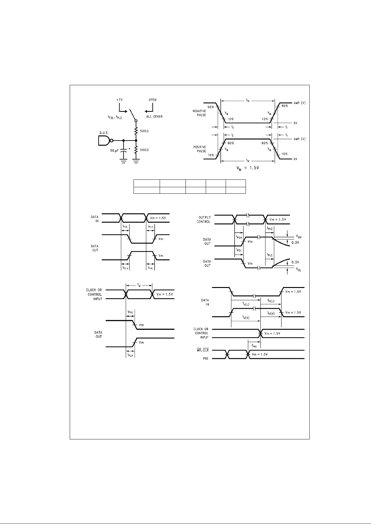
AC Loading
*Includes jig and pr obe capacitance
FIGURE 1. Standard AC Test Load
FIGURE 2. Test Input Signal Levels
FIGURE 3. Test Input Signal Requirements
AC Waveforms
FIGURE 4. Propagation Delay Waveforms for
Inverting and Non-Inverting Functions
FIGURE 5. Propagation Delay,
Pulse Width Waveforms
FIGURE 6. 3-STA TE Output HIGH
and LOW Enable and Disable Times
FIGURE 7. Setup Time, Hold Time
and Recovery Time Waveforms
Amplitude Rep. Rate t
w
t
r
t
f
3.0V 1 MHz 500 ns 2.5 ns 2.5 ns
Page 7

7 www.fairchildsemi.com
74ABT373
Physical Dimensions inches (millimeters) unless otherwise noted
20-Lead Small Outline Integrated Circuit (SOIC), JEDEC MS-013, 0.300” Wide Body
Package Number M20B
Page 8

www.fairchildsemi.com 8
74ABT373
Physical Dimensions inches (millimeters) unless otherwise noted (Continued)
20-Lead Small Outline Package (SOP), EIAJ TYPE II, 5.3mm Wide
Package Number M20D
Page 9

9 www.fairchildsemi.com
74ABT373
Physical Dimensions inches (millimeters) unless otherwise noted (Continued)
20-Lead Shrink Small Outline Package (SSOP), EIAJ TYPE II, 5.3mm Wide
Package Num b er MSA20
Page 10

www.fairchildsemi.com 10
74ABT373
Physical Dimensions inches (millimeters) unless otherwise noted (Continued)
20-Lead Thin Shrink Small Outline Package (TSSOP), JEDEC MO-153, 4.4mm Wide
Package Number MTC20
Page 11

11 www.fairchildsemi.com
74ABT373 Octal Transparent Latch with 3-STATE Outputs
Physical Dimensions inches (millimeters) unless otherwise noted (Continued)
20-Lead Plastic Dual-In-Line Package (PDIP), JEDEC MS-001, 0.300” Wide
Package Number N20A
Fairchild does not assume any responsibility for use of any circuitry described , no circuit patent licenses are implied and
Fairchild reserves the right at any time without notice to change said circuitry and specifications.
LIFE SUPPORT POLICY
FAIRCHILD’S PRODUCTS ARE NOT AUTHORIZED FOR USE AS CRITICAL COMPONENTS IN LIFE SUPPORT
DEVICES OR SYSTEMS WITHOUT THE EXPRESS WRITTEN APPROVAL OF THE PRESIDENT OF FAIRCHILD
SEMICONDUCTOR CORPORATION. As used herein:
1. Life support devices or systems are dev ic es or syste ms
which, (a) are intended for surgical implant into the
body, or (b) support or sustain life, and (c) whose failure
to perform when properly used in accordance with
instructions for use provide d in the labe l ing, can be re asonably expected to result in a significant injury to the
user.
2. A critical compo nent in any com ponen t of a life s upp ort
device or system whose failure to perform can be reasonably expected to cause the failure of the l ife s upport
device or system, or to affect its safety or effectiveness.
www.fairchildsemi.com
 Loading...