

Datasheet 74ABT245CMSA, 74ABT245CSJX, 74ABT245CSJ, 74ABT245CSCX, 74ABT245CSC Datasheet (Fairchild Semiconductor)
...Page 1
© 1999 Fairchild Semiconductor Corporation DS010945 www.fairchildsemi.com
September 1991
Revised November 1999
74ABT245 Octal Bi-Directional Transceiver with 3-STATE Outputs
74ABT245
Octal Bi-Directional Transceiver with 3-STATE Outputs
General Description
The ABT245 contains eight non-inverting bidirectional buffers with 3-STATE outputs and is intended fo r bus-or iented
applications. Current sinking capability is 64 mA on bo th
the A and B ports. The Transmit/Receive (T/R
) input determines the direction of data flow through the bidirectional
transceiver. Transmit (active HIGH) enables data from A
Ports to B Ports; Re ceive (activ e LOW) en ables data from
B Ports to A Ports. T he Output Enab le input, wh en HIGH,
disables both A and B ports b y placing them in a H IGH Z
condition.
Features
■ Bidirectional non-inverting buffers
■ A and B output sink capability of 64 mA, source
capability of 32 mA
■ Guaranteed output ske w
■ Guaranteed multiple output switching specifications
■ Output switching sp ecified for both 50 pF and 250 pF
loads
■ Guaranteed simultaneous switching, noise level and
dynamic threshold performan ce
■ Guarante ed latchup protection
■ High impedance glitch-free bus loading during entire
power up and power down cycle
■ Non-destructive hot insertion capability
■ Disable time is less than enable time to avoid bus
contention
Ordering Code:
Device also available in Tape and Reel. Specify by appending s uffix let te r “X” to the ordering code.
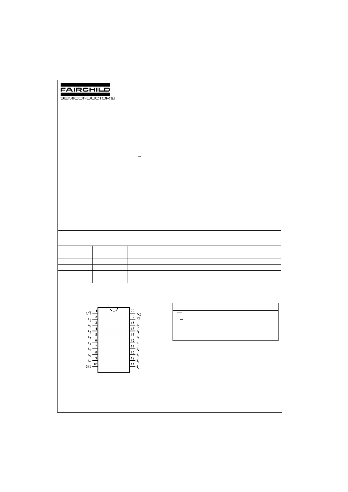
Connection Diagram Pin Descriptions
Order Number Package Number Package Description
74ABT245CSC M20B 20-Lead Small Outline Integrated Circuit (SOIC), JEDEC MS-013, 0.300” Wide Body
74ABT245CSJ M20D 20-Lead Small Outline Package (SOP), EIAJ TYPE II, 5.3mm Wide
74ABT245CMSA MSA20 20-Lead Shrink Small Outline Package (SSOP), EIAJ TYPE II, 5.3mm Wide
74ABT245CMTC MTC20 20-Lead Thin Shrink Small Outline Package (TSSOP), JEDEC MO-153, 4.4mm Wide
74ABT245CPC N20A 20-Lead Plastic Dual-In-Line Package (PDIP), JEDEC MS-001, 0.300” Wide
Pin Names Description
OE
Output Enable Input (Active LOW)
T/R
Transmit/Receive Input
A
0–A7
Side A Inputs or 3-STATE Outputs
B
0–B7
Side B Inputs or 3-STATE Outputs
Page 2
www.fairchildsemi.com 2
74ABT245
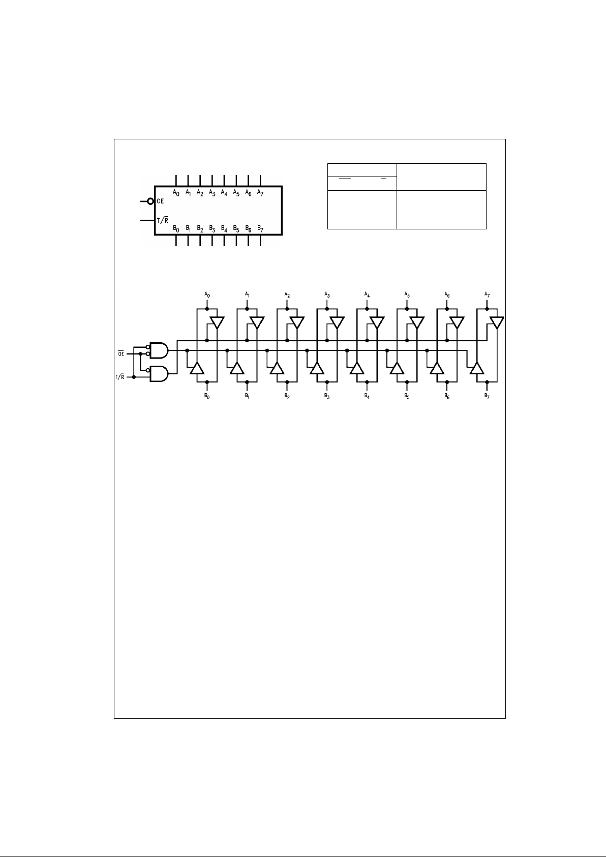
Logic Symbol Truth Table
H = HIGH Voltage Level
L = LOW Voltage Level
X = Immaterial
Logic Diagram
Inputs Output
OE T/R
L L Bus B Data to Bus A
L H Bus A Data to Bus B
H X HIGH Z State
Page 3
3 www.fairchildsemi.com
74ABT245
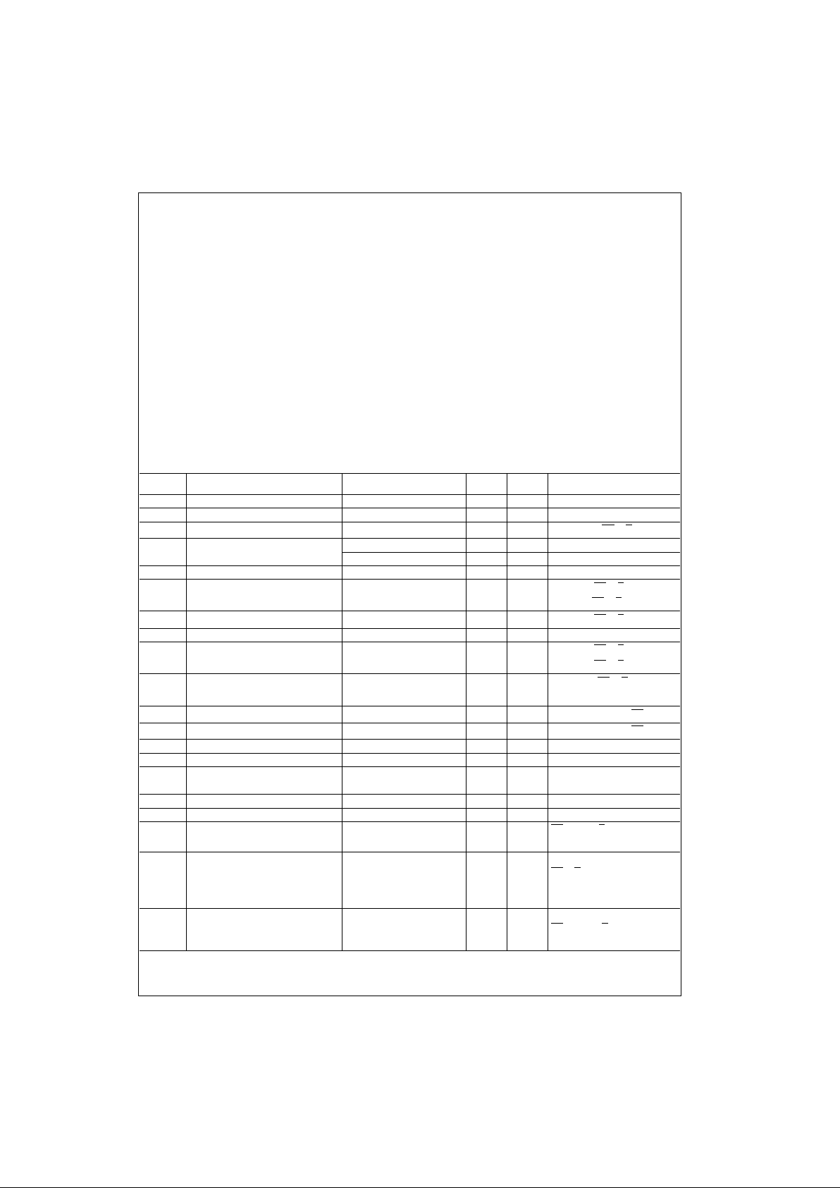
Absolute Maximum Ratings(Note 1) Recommended Operating
Conditions
Note 1: Absolute maximum ratings are values beyond which the device
may be damaged or have its useful life impaired . Functional operation
under these conditions is not implied.
Note 2: Either voltage lim it or c urrent limit is sufficient to pro te c t in puts
DC Electrical Characteristics
Storage Temperature −65°C to +150°C
Ambient Temperature under Bias −55°C to +125°C
Junction Temperature under Bias −55°C to +150°C
V
CC
Pin Potential to Ground Pin −0.5V to +7.0V
Input Voltage (Note 2) −0.5V to +7.0V
Input Current (Note 2) −30 mA to +5.0 mA
Voltage Applied to Any Output
in the Disabled or
Power-off State −0.5V to 5.5V
in the HIGH State −0.5V to V
CC
Current Applied to Output
in LOW State (Max) twice the rated I
OL
(mA)
DC Latchup Source Current −500 mA
Over Voltage Latchup (I/O) 10V
Free Air Ambient Temperature −40°C to +85°C
Supply Voltage +4.5V to +5.5V
Minimum Input Edge Rate (∆V/∆t)
Data Input 50 mV/ns
Enable Input 20 mV/ns
Symbol Parameter Min Typ Max Units
V
CC
Conditions
V
IH
Input HIGH Voltage 2.0 V Recognized HIGH Signal
V
IL
Input LOW Voltage 0.8 V Recognized LOW Signal
V
CD
Input Clamp Diode Voltage −1.2 V Min
IIN = −18 mA (OE, T/R)
V
OH
Output HIGH Voltage 2.5 V Min IOH = −3 mA (An, Bn)
2.0 V Min IOH = −32 mA (An, Bn)
V
OL
Output LOW Voltage 0.55 V Min IOL = 64 mA (An, Bn)
I
IH
Input HIGH Current 1
µAMax
VIN = 2.7V (OE, T/R)
1
VIN = VCC (OE, T/R)
I
BVI
Input HIGH Current Breakdown Test 7 µAMax
V
IN
= 7.0V (OE, T/R)
I
BVIT
Input HIGH Current Breakdown Test (I/O) 100 µAMaxVIN = 5.5V (An, Bn)
I
IL
Input LOW Current −1
µAMax
V
IN
= 0.5V (OE, T/R)
−1
V
IN
= 0.0V (OE, T/R)
V
ID
Input Leakage Test 4.75 V 0.0
IID = 1.9 µA (OE, T/R)
All Other Pins Grounded
I
IH
+ I
OZH
Output Leakage Current 10 µA0 − 5.5V
V
OUT
= 2.7V (An, Bn); OE = 2.0V
I
IL
+ I
OZL
Output Leakage Current −10 µA0 − 5.5V
V
OUT
= 0.5V (An, Bn); OE = 2.0V
I
OS
Output Short-Circuit Current −100 −275 mA Max V
OUT
= 0.0V (An, Bn)
I
CEX
Output HIGH Leakage Current 50 µAMaxV
OUT
= V
CC
(An, Bn)
I
ZZ
Bus Drainage Test 100 µA0.0V
OUT
= 5.5V (An, Bn);
All Others GND
I
CCH
Power Supply Current 50 µA Max All Outputs HIGH
I
CCL
Power Supply Current 30 mA Max All Outputs LOW
I
CCZ
Power Supply Current 50 µAMax
OE = VCC, T/R = GND or VCC;
All Other GND or V
CC
I
CCT
Additional Outputs Enabled 2.5 mA VI = V
CC
− 2.1V
I
CC
/Input Outputs 3-STATE 2.5 mA Max
OE, T/R VI = VCC − 2.1V
Outputs 3-STATE 50 µA Data Input VI = VCC − 2.1V
All Others at VCC or GND.
I
CCD
Dynamic I
CC
No Load 0.1 mA/
Max
Outputs Open
MHz
OE = GND, T/R = GND or V
CC
One Bit Toggling, 50% Duty Cycle
Page 4
www.fairchildsemi.com 4
74ABT245
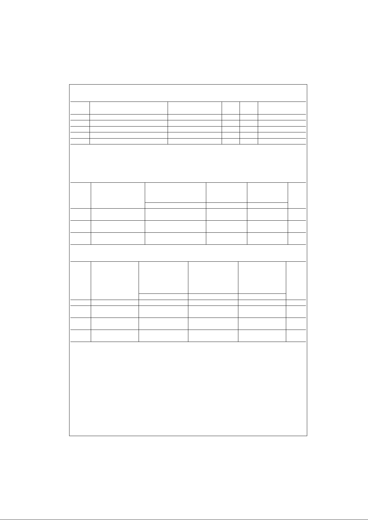
DC Electrical Characteristics
(SOIC package)
Note 3: Max number of outputs defined as (n). n-1 data inputs are driven 0V to 3V. One output at LOW. Guaranteed, but not tested.
Note 4: Max number of data inputs (n) switching. n-1 inputs switching 0V to 3V. Input-under-test switching: 3V to threshold (V
ILD
), 0V to threshold (V
IHD
).
Guaranteed, but not tested.
Note 5: Max number of output s d ef ined as (n). n − 1 data inputs are driven 0V to 3V. One output HIGH. Guaranteed, but not tested.
AC Electrical Characteristics
(SOIC and SSOP package)
Extended AC Electrical Characteristics
(SOIC package)
Note 6: This specification is gu aranteed but not tested . The limits apply to propagation delays for all paths described switching in ph ase
(i.e., all LOW-to-HIGH, HIGH-to-LOW, etc.).
Note 7: This specification is guaranteed but not tested. The limits represent propagation delay with 250 pF load capacitors in place of the 50 pF load capacitors in the standard AC load. This specifica ti on pertains to single output switching only.
Note 8: This specification is gu aranteed but not tested . The limits represent propagation delays for all pa t hs des c ribed switching in phase
(i.e., all LOW-to-HIGH, HIGH-to-LOW, etc.) with 250 pF load capacitors in place of the 50 pF load capacitors in the standard AC load.
Note 9: The 3-STATE delays are dominated by the RC network (500Ω, 250 pF) on the output and have been excluded from the datasheet.
Symbol Parameter Min Typ Max Units
V
CC
Conditions
CL = 50 pF, RL = 500Ω
V
OLP
Quiet Output Maximum Dynamic V
OL
0.7 1.0 V 5.0 TA = 25°C (Note 3)
V
OLV
Quiet Output Minimum Dynamic V
OL
−1.3 −1.0 V 5.0 TA = 25°C (Note 3)
V
OHV
Minimum HIGH Level Dynamic Output Voltage 2.7 3.1 V 5.0 TA = 25°C (Note 5)
V
IHD
Minimum HIGH Level Dynamic Input Voltage 2.0 1.7 V 5.0 TA = 25°C (Note 4)
V
ILD
Maximum LOW Level Dynamic Input Voltage 0.9 0.6 V 5.0 TA = 25°C (Note 4)
TA = +25°CT
A
= −55°C to +125°CTA = −40°C to +85°C
Symbol Parameter
V
CC
= +5V VCC = 4.5V–5.5V VCC = 4.5V–5.5V
Units
CL = 50 pF CL = 50 pF CL = 50 pF
Min Typ Max Min Max Min Max
t
PLH
Propagation Delay 1.0 2.1 3.6 1.0 4.8 1.0 3.6
ns
t
PHL
Data to Outputs 1.0 2.4 3.6 1.0 4.8 1.0 3.6
t
PZH
Output Enable 1.5 3.2 6.0 1.0 6.7 1.5 6.0
ns
t
PZL
Time 1.5 3.7 6.0 2.0 7.5 1.5 6.0
t
PHZ
Output Disable 1.0 3.6 6.1 1.7 7.4 1.0 6.1
ns
t
PLZ
Time 1.0 3.3 5.6 1.7 6.5 1.0 5.6
Symbol Parameter
−40°C to +85°C
TA = −40°C to +85°C T
A
= −40°C to +85°C
Units
VCC = 4.5V–5.5V VCC = 4.5V–5.5V VCC = 4.5V–5.5V
CL = 50 pF CL = 250 pF CL = 250 pF
8 Outputs Switching 1 Output Switching 8 Outputs Switching
(Note 6) (Note 7) (Note 8)
Min Typ Max Min Max Min Max
f
TOGGLE
Max Toggle Frequency 100 MHz
t
PLH
Propagation Delay 1.5 5.0 1.5 6.0 2.5 8.5
ns
t
PHL
Data to Outputs 1.5 5.0 1.5 6.0 2.5 8.5
t
PZH
Output Enable Time 1.5 6.5 2.5 7.5 2.5 9.5
ns
t
PZL
1.5 6.5 2.5 7.5 2.5 11.0
t
PHZ
Output Disable Time 1.0 6.5
(Note 9) (Note 9) ns
t
PLZ
1.0 5.6
Page 5

5 www.fairchildsemi.com
74ABT245
Skew
(SOIC package)
Note 10: Skew is def ined as the absolu te valu e of the differ ence be tween the actu al propag ation de lays f or any tw o separ ate outpu ts of the sam e devi ce.
The specification ap plies to any outputs switc hing HIGH-to-LOW (t
OSHL
), LOW-to-HIGH (t
OSLH
), or any combination switching LOW-to-HIGH and/or
HIGH
-to-LOW (t
OST
). The specification is guaranteed but not test ed.
Note 11: Propagation delay variation for a given set of conditions (i. e. , te m perature and V
CC
) from device to device. This specification is guaranteed but not
tested.
Note 12: This specification is guaranteed but not tested. The limits apply to propagation delays for all paths described switching in phase
(i.e., all LOW-to-HIGH, HIGH-to-LOW, etc.)
Note 13: These specific ations gua ranteed b ut not tes ted. The limits repr esent propa gation de lays with 250 pF lo ad capacit ors in pla ce of the 50 pF load
capacitors in the standard AC load.
Note 14: This describ es th e d ifferenc e b etw een t he del ay o f t he LO W-to -HIGH an d the HIGH -to -LOW tra nsitio n on t he s ame p in. It is mea sure d across all
the outputs (drivers) on t he same chip, the worst (la rgest delta) number is the guaranteed specificat ion. This specification is guaranteed but not tested.
Capacitance
Note 15: C
I/O
is measured at frequency f = 1 MHz, per MIL-STD-883, Me t hod 3012.
Symbol Parameter
TA = −40°C to +85°CT
A
= −40°C to +85°C
Units
VCC = 4.5V–5.5V VCC = 4.5V–5.5V
CL = 50 pF CL = 250 pF
8 Outputs Switching 8 Outputs Switching
(Note 12) (Note 13)
Max Max
t
OSHL
Pin to Pin Skew
1.3 2.3 ns
(Note 10) HL Transitions
t
OSLH
Pin to Pin Skew
1.0 1.8 ns
(Note 10) LH Transitions
t
PS
Duty Cycle
2.0 3.5 ns
(Note 14) LH–HL Skew
t
OST
Pin to Pin Skew
2.0 3.5 ns
(Note 10) LH/HL Transitions
t
PV
Device to Device Skew
2.0 3.5 ns
(Note 11) LH/HL Transitions
Symbol Parameter Typ Units
Conditions
TA = 25°C
C
IN
Input Capacitance 5.0 pF VCC = 0V (OE, T/R)
C
I/O
(Note 15) I/O Capacitance 11.0 pF VCC = 5.0V (An, Bn)
Page 6

www.fairchildsemi.com 6
74ABT245
AC Loading
*Includes jig and pr obe capacitance
FIGURE 1. Standard AC Test Load
FIGURE 2. Test Input Signal Levels
FIGURE 3. Test Input Signal Requirements
AC Waveforms
FIGURE 4. Propagation Delay Waveforms
for Inverting and Non-Inverting Functions
FIGURE 5. Propagation Delay,
Pulse Width Waveforms
FIGURE 6. 3-STA TE Output HIGH
and LOW Enable and Disable Times
FIGURE 7. Setup Time, Hold Time
and Recovery Time Waveforms
Amplitude Rep. Rate t
W
t
r
t
f
3.0V 1 MHz 500 ns 2.5 ns 2.5 ns
Page 7

7 www.fairchildsemi.com
74ABT245
Physical Dimensions inches (millimeters) unless otherwise noted
20-Lead Small Outline Integrated Circuit (SOIC), JEDEC MS-013, 0.300” Wide Body
Package Number M20B
Page 8

www.fairchildsemi.com 8
74ABT245
Physical Dimensions inches (millimeters) unless otherwise noted (Continued)
20-Lead Small Outline Package (SOP), EIAJ TYPE II, 5.3mm Wide
Package Number M20D
Page 9

9 www.fairchildsemi.com
74ABT245
Physical Dimensions inches (millimeters) unless otherwise noted (Continued)
20-Lead Shrink Small Outline Package (SSOP), EIAJ TYPE II, 5.3mm Wide
Package Num b er MSA20
Page 10

www.fairchildsemi.com 10
74ABT245
Physical Dimensions inches (millimeters) unless otherwise noted (Continued)
20-Lead Thin Shrink Small Outline Package (TSSOP), JEDEC MO-153, 4.4mm Wide
Package Number MTC20
Page 11

11 www.fairchildsemi.com
74ABT245 Octal Bi-Directional Transceiver with 3-STATE Outputs
Physical Dimensions inches (millimeters) unless otherwise noted (Continued)
20-Lead Plastic Dual-In-Line Package ( PDIP), JEDEC MS -001, 0.300” Wide
Package Number N20A
Fairchild does not assume any responsibility for use of any circuitry described , no circuit patent licenses are implied and
Fairchild reserves the right at any time without notice to change said circuitry and specifications.
LIFE SUPPORT POLICY
FAIRCHILD’S PRODUCTS ARE NOT AUTHORIZED FOR USE AS CRITICAL COMPONENTS IN LIFE SUPPORT
DEVICES OR SYSTEMS WITHOUT THE EXPRESS WRITTEN APPROVAL OF THE PRESIDENT OF FAIRCHILD
SEMICONDUCTOR CORPORATION. As used herein:
1. Life support devices or systems are dev ic es or syste ms
which, (a) are intended for surgical implant into the
body, or (b) support or sustain life, and (c) whose failure
to perform when properly used in accordance with
instructions for use provide d in the labe l ing, can be re asonably expected to result in a significant injury to the
user.
2. A critical compo nent in any com ponen t of a life s upp ort
device or system whose failure to perform can be reasonably expected to cause the failure of the l ife support
device or system, or to affect its safety or effectiveness.
www.fairchildsemi.com
 Loading...