

Datasheet 74ABT16500CSSCX, 74ABT16500CSSC, 74ABT16500CMTDX, 74ABT16500CMTD Datasheet (Fairchild Semiconductor)
Page 1
April 1993
Revised January 1999
74ABT16500 18-Bit Universal Bus Transceivers with 3-STATE Outputs
© 1999 Fairchild Semiconductor Corporation DS011581.prf www.fairchildsemi.com
74ABT16500
18-Bit Universal Bus Transceivers with 3-STATE Outputs
General Description
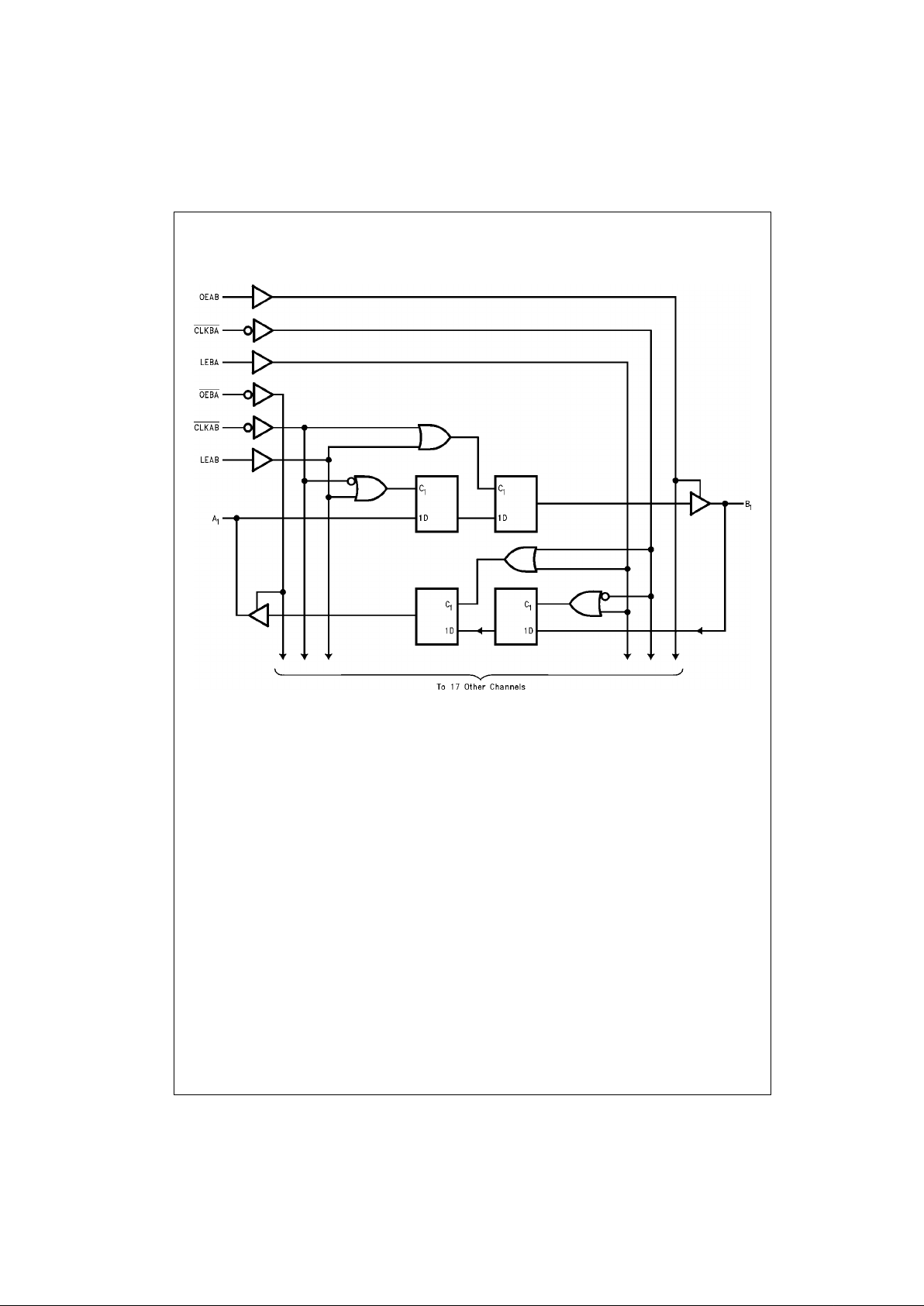
The ABT16500 18-bit u niversal bus transceiver combines
D-type latches and D-type flip-flops to allow data flow in
transparent, latched, and clocked modes.
Data flow in each direction is contr olled by output-enable
(OEAB and OEBA
), latch-enable (LEAB and LEBA), and
clock (CLKAB
and CLKBA) inputs. For A-to-B data flow, the
device operates in the transparent mode when LEAB is
HIGH. When LEAB is LOW, the A data is latched if CLKAB
is held at a HIGH or LOW logic level. If LEAB is LOW, the A
bus data is stored in the latch/flip-flop on the HIGH-to-LOW
transition of CLKAB
. Output-enable OEAB is active-high.
When OEAB is HIGH, the outputs are active. When OEAB
is LOW, the outputs are in the high-impedance state.
Data flow for B to A is similar to tha t of A to B but uses
OEBA
, LEBA, and CLKBA. The output enables ar e com-
plementary (OEAB is active HIGH and OEBA
is active
LOW).
To ensure the high-imp edance state during power up or
power down, OE should be tied to GN D t hr o ug h a pulldown
resistor; the minimum value of the resistor is determined by
the current-sourcing capability of the driver.
Features
■ Combines D-Type latches and D-Type flip-flops for
operation in transparent, latched, or clocked mode
■ Flow-through architecture optimizes PCB layout
■ Guaranteed latch-up protection
■ High impedance glitch free bus loading during entire
power up and power down cycle
■ Non-destructive hot insertion capability
Ordering Code:
Devices also available in Tape and Reel. Specify by appending the letter suffix “X” to t he ordering code.
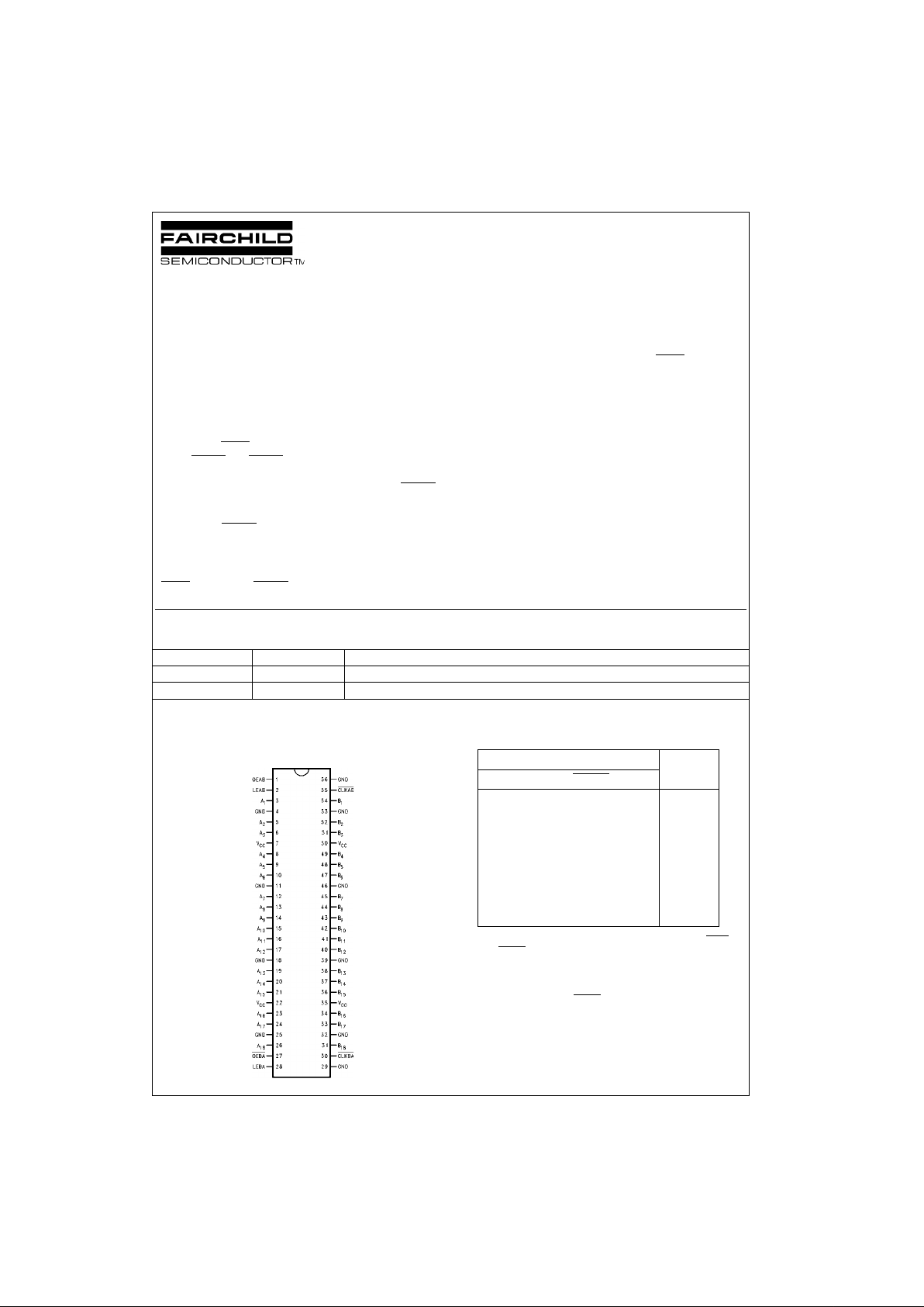
Connection Diagram
Pin Assign ment for SSOP
Function Table (Note 1)
Note 1: A-to-B data flow is s hown: B-to-A flow is similar but use s OEBA,
LEBA, and CLKBA
.
Note 2: Output level before the indicated s teady-state input conditions
were established.
Note 3: Output level before the indicated s teady-state input conditions
were established, provid ed t hat CLKAB
was LOW before LEAB went LOW.
Order Number Package Number Package Description
74ABT16500CSSC MS56A 56-Lead Shrink Small Outline Package (SSOP), JEDEC MO-118, 0.300” Wide
74ABT16500CMTD MTD56 56-Lead Thin Shrink Small Outline Package (TSSOP), JEDEC MO-153, 6.1mm Wide
Inputs Output
OEAB LEAB CLKAB
AB
LXXX Z
HHXL L
HHXH H
HL↓ LL
HL↓ HH
HLHXB
0
(Note 2)
HLLXB
0
(Note 3)
Page 2
www.fairchildsemi.com 2
74ABT16500
Logic Diagram
Page 3
3 www.fairchildsemi.com
74ABT16500
Absolute Maximum Ratings(Note 4)
Recommended Operating
Conditions
Note 4: Absolute maximum ratings are values beyond which the device
may be damaged or have its useful life impaired. Functional operation
under these condit ions is not implied.
Note 5: Either voltage limit or current limi t is s uf f ic ient to protect inputs.
DC Electrical Characteristics
Note 6: Guaranteed, but not tested.
Storage Temperature −65°C to +150°C
Ambient Temperature under Bias −55°C to +125°C
Junction Temperature under Bias −55°C to +150°C
V
CC
Pin Potential to
Ground Pin −0.5V to +7.0V
Input Voltage (Note 5) −0.5V to +7.0V
Input Current (Note 5) −30 mA to +5.0 mA
Voltage Applied to Any Output
in the Disabled or
Power-off State −0.5V to 5.5V
in the HIGH State −0.5V to V
CC
Current Applied to Output
in LOW State (Max) twice the rated I
OL
(mA)
DC Latchup Source Current −500 mA
Over Voltage Latchup (I/O) 10V
Free Air Ambient Temperature −40°C to +85°C
Supply Voltage +4.5V to +5.5V
Minimum Input Edge Rate (∆V/∆t)
Data Input 50 mV/ns
Enable Input 20 mV/ns
Symbol Parameter Min Typ Max Units
V
CC
Conditions
V
IH
Input HIGH Voltage 2.0 V Recognized HIGH Signal
V
IL
Input LOW Vo ltage 0.8 V Recognized LOW Signal
V
CD
Input Clamp Diode Voltage −1.2 V Min IIN = −18 mA
V
OH
Output HIGH Voltage 2.5 V Min IOH = −3 mA
2.0 V Min IOH = −32 mA
V
OL
Output LOW Voltage 0.55 V Min IOL = 64 mA
I
IH
Input HIGH Current 1 µAMaxVIN = 2.7V (Note 6)
1V
IN
= V
CC
I
BVI
Input HIGH Current Breakdown Test 7 µAMaxVIN = 7.0V
I
IL
Input LOW Current −1 µAMaxVIN = 0.5V (Note 6)
−1V
IN
= 0.0V
V
ID
Input Leakage Test 4.75 V 0.0 IID = 1.9 µA
All Other Pins Grounded
IIH + Output Leakage Current
10 µA0 − 5.5V
V
OUT
= 2.7V; OE, OE = 2.0V
I
OZH
IIL + Output Leakage Current
−10 µA0 − 5.5V
V
OUT
= 0.5V; OE, OE = 2.0V
I
OZL
I
OS
Output Short-Circuit Current −100 −275 mA Max V
OUT
= 0V
I
CEX
Output HIGH Leakage Current 50 µAMaxV
OUT
= V
CC
I
ZZ
Bus Drainage Test 100 µA0.0V
OUT
= 5.5V; All Others GND
I
CCH
Power Supply Current 1.0 mA Max All Outputs HIGH
I
CCL
Power Supply Current 68 µA Max An or Bn Outputs Low
I
CCZ
Power Supply Current
1.0 mA Max
OEn = VCC,
All Others at VCC or GND
I
CCT
Additional ICC/Input 2.5 mA Max VI = VCC − 2.1V
All Others at VCC or GND
I
CCD
Dynamic I
CC
No Load mA/ Max Outputs Open
(Note 6) 0.23 MHz Transparent Mode
One Bit Toggling, 50% Duty Cycle
Page 4

www.fairchildsemi.com 4
74ABT16500
DC Electrical Characteristics
Note 7: Max number of outputs defined as (n) . n − 1 dat a inputs are driven 0V to 3V. One output at LOW. Guaranteed, but not te s te d.
Note 8: Max number of outputs defined as (n) . n − 1 dat a inputs are driven 0V to 3V. One output HIGH. Guaranteed, but not tested.
Note 9: Max number of data i npu ts (n) swit chin g. n − 1 inpu ts switc hing 0 V to 3 V. Input-under-test switc hing: 3V t o thr esho ld (V
ILD
), 0V to threshold (V
IHD
).
Guaranteed, but not tes t ed.
AC Electrical Charac teristics
Symbol Parameter Min Typ Max Units
V
CC
Conditions
CL = 50 pF; RL = 500Ω
V
OLP
Quiet Output Maximum Dynamic V
OL
0.7 1.2 V 5.0 TA = 25°C (Note 7)
V
OLV
Quiet Output Minimum Dynamic V
OL
−1.5 −1.0 V 5.0 TA = 25°C (Note 7)
V
OHV
Minimum HIGH Level Dynamic Output Voltage 2.5 3.0 V 5.0 TA = 25°C (Note 8)
V
IHD
Minimum HIGH Level Dynamic Input Voltage 2.2 1.8 V 5.0 TA = 25°C (Note 9)
V
ILD
Maximum LOW Level Dynamic Input Voltage 1.2 0.8 V 5.0 TA = 25°C (Note 9)
Symbol P a rameter
TA = +25°CT
A
= −40°C to +85°C
Units
VCC = +5V VCC = 4.5V–5.5V
CL = 50 pF CL = 50 pF
Min Typ Max Min Max
f
max
Maximum Clock Frequency 150 200 150 MHz
t
PLH
Propagation Delay 1.5 2.7 4.6 1.5 4.6 ns
t
PHL
A or B to B or A 1.5 3.2 4.6 1.5 4.6
t
PLH
Propagation Delay 1.5 3.1 5.0 1.5 5.0 ns
t
PHL
LEAB or LEBA to B or A 1.5 3.6 5.0 1.5 5.0
t
PLH
Propagation Delay 1.5 3.4 5.3 1.5 5.3 ns
t
PHL
CLKAB or CLKBA to B or A
1.5 3.7 5.3 1.5 5.3
t
PZH
Propagation Delay 1.5 2.7 5.6 1.5 5.6 ns
t
PZL
OEAB or OEBA to B or A
1.5 3.0 5.6 1.5 5.6
t
PHZ
Propagation Delay 1.5 3.7 6.0 1.5 6.0 ns
t
PLZ
OEAB or OEBA to B or A
1.5 3.2 6.0 1.5 6.0
Page 5

5 www.fairchildsemi.com
74ABT16500
AC Operating Requirements
Extended AC Electri cal Characteristics
Note 10: This specific at ion is guaranteed but not test ed. The limits apply to pr opagation delays for all paths desc ribed switching in phase
(i.e., all LOW-to-HIGH, HIGH-to-LOW, etc.).
Note 11: This specification is guaranteed but not tested. The limits represent propagation delay with 250 pF load capacitors in place of the 50 pF load capac-
itors in the standard AC load . Th is sp ec if ic ation pertains to sin gle output switching only.
Note 12: This specific at ion is guaranteed but not test ed. The limits represent propagation delays for all paths described switching in phase
(i.e., all LOW-to-HIGH, HIGH-to-LOW, etc.) with 250 pF load capacitors in plac e of th e 50 pF load capacitors in t he s t andard AC load.
Note 13: 3-STATE delays are dominated by the RC network (500Ω, 250 pF ) on the output and have been excluded from the datashe et .
Symbol Parameter
TA = +25°CT
A
= −40°C to +85°C
Units
VCC = +5V VCC = 4.5V–5.5V
CL = 50 pF CL = 50 pF
Min Max Min Max
tS(H) Setup Time, 4.5 4.5 ns
tS(L)
A to CLKAB
4.5 4.5
tH(H) Hold Time, 0 0 ns
tH(L)
A to CLKAB
00
tS(H) Setup Time, 4.0 4.0 ns
tS(L)
B to CLKBA
4.0 4.0
tH(H) Hold Time, 0 0 ns
tH(L)
B to CLKBA
00
tS(H) Setup Time, A to LEAB 1.5 1.5 ns
tS(L)
or B to LEBA, CLK HIGH
1.5 1.5
tH(H) Hold Time, A to LEAB 1.5 1.5
ns
tH(L)
or B to LEBA, CLK HIGH
1.5 1.5
tS(H) Setup Time, A to LEAB 4.5 4.5 ns
tS(L)
or B to LEBA, CLK LOW
4.5 4.5
tH(H) Hold Time, A to LEAB 1.5 1.5 ns
tH(L)
or B to LEBA, CLK LOW
1.5 1.5
tW(H) Pulse Width, 3.3 3.3 ns
tW(L) LEAB or LEBA, HIGH 3.3 3.3
tW(H)
Pulse Width, CLKAB
3.3 3.3
ns
tW(L)
or CLKBA, HIGH or LOW
3.3 3.3
Symbol Parameter
TA = −40°C to +85°CT
A
= −40°C to +85°CTA = −40°C to +85°C
Units
VCC = 4.5V–5.5V VCC = 4.5V–5.5V VCC = 4.5V–5.5V
CL = 50 pF CL = 250 pF CL = 250 pF
18 Outputs Switching 1 Output Switching 18 Outputs Switching
(Note 10) (Note 11) (Note 12)
Min Typ Max Min Max Min Max
t
PLH
Propagation Delay 1.5 6.5 2.0 7.0 2.5 9.9
ns
t
PHL
Data to Outputs 1.5 6.5 2.0 7.0 2.5 9.2
t
PLH
Propagation Delay 1.5 6.0 2.0 7.5 2.5 8.5
ns
t
PHL
LEAB or LEBA to B or A 1.5 6.0 2.0 7.5 2.5 8.5
t
PLH
Propagation Delay 1.5 6.2 2.0 7.7 2.5 8.5
ns
t
PHL
CLKAB or CLKBA to B or A
1.5 6.2 2.0 7.7 2.5 8.5
t
PZH
Output Enable Time 1.5 6.5 2.0 7.0 2.5 8.5
ns
t
PZL
1.5 6.5 2.5 7.0 2.5 8.5
t
PHZ
Output Disable 1.5 6.5 (Note 13) (Note 13)
ns
t
PLZ
Time 1.5 6.5
Page 6

www.fairchildsemi.com 6
74ABT16500
Skew
Note 14: This spec if ic at ion is guaranteed but not test ed. The limits apply to pro pagation delays for all paths desc ribed switching in phase
(i.e., all LOW-to-HIGH, HIGH-to-LOW, etc.)
Note 15: These specifica tions gu aranteed but n ot tested . The lim its represe nt propagat ion delays w ith 250 p F load cap acitors in place of the 50 pF lo ad
capacitors in the standard AC load.
Note 16: Skew is defined as the ab solute valu e of the difference betwe en the actual p ropag ation d elays for any tw o sepa rate outp uts of the same device.
The specificatio n applies to any out puts switching HIGH- to-LOW (t
OSHL
), LOW-to-HIGH (t
OSLH
), or any combination swit ching L OW-to-HIGH and /or HIGH-
to-LOW (t
OST
). The specification is guaranteed but not tested.
Note 17: This descr ibes the difference bet ween the de lay of the LOW-to-HIGH and the HI GH-to-LOW transition on the sam e pin. It is me asured a cros s all
the outputs (drivers ) on the same chip, the worst (larg es t delta) number is the guarant eed specification. T his s pecification is guaranteed but not t es t ed.
Note 18: Propagation delay variation for a given set of conditions (i.e., temperature and VCC) from device to device. T his specification is guaranteed but not
tested.
Capacitance
Note 19: C
I/O
is measured at frequency f = 1 MHz per MIL-STD-883, Method 3012.
Symbol Parameter
TA = −40°C to +85°CT
A
= −40°C to +85°C
Units
VCC = 4.5V–5.5V VCC = 4.5V–5.5V
CL = 50 pF CL = 250 pF
18 Outputs Switching 18 Outputs Switching
(Note 14) (Note 15)
Max Max
t
OSHL
Pin to Pin Skew 2.0 2.8
ns
(Note 16) HL Transitions
t
OSLH
Pin to Pin Skew 2.0 2.5
ns
(Note 16) LH Transitions
t
PS
Duty Cycle 2.0 2.8
ns
(Note 17) LH–HL Skew
t
OST
Pin to Pin Skew 2.5 3.0
ns
(Note 16) LH/HL Transitions
t
PV
Device to Device Skew 3.0 3.5
ns
(Note 18) LH/HL Transitions
Symbol Parameter Typ Units
Conditions
TA = 25°C
C
IN
Input Capacitance 5.0 pF VCC = 0.0V
C
I/O
(Note 19) Output Capacitance 11.0 pF VCC = 5.0V
Page 7

7 www.fairchildsemi.com
74ABT16500
AC Loading
*Includes jig and prob e c apacitance.
FIGURE 1. Standard AC Test Load
FIGURE 2. V
M
= 1.5V
Input Pulse Requirement s
FIGURE 3. Test Input Signal Requirements
AC Waveforms
FIGURE 4. Propagation Delay Waveforms
for Inverting and Non-Inverting Functions
FIGURE 5. Propagation Delay,
Pulse Width W aveforms
FIGURE 6. 3-STATE Output HIGH
and LOW Enable and Disable Times
FIGURE 7. Setup Time, Hold Time
and Recovery Time Waveforms
Amplitude Rep. Rate t
W
t
r
t
f
3.0V 1 MHz 500 ns 2.5 ns 2.5 ns
Page 8

www.fairchildsemi.com 8
74ABT16500
Physical Dimensions inches (millimeters) unless otherwise noted
56-Lead Shrink Small Outline Package (SSOP), JEDEC MO-118, 0.300” Wide
Package Number MS56A
Page 9

Fairchild does not assume any responsibility for use of any circuitry described, no circuit patent licenses are implied and Fairchild reser ves the right at any time without notice to change said circuitry and specifications.
74ABT16500 18-Bit Universal Bus Transceivers with 3-STATE Outputs
LIFE SUPPORT POLICY
FAIRCHILD’S PRODUCTS ARE NOT AUTHORIZED FOR USE AS CRITICAL COMPONENTS IN LIFE SUPPORT
DEVICES OR SYSTEMS WITHOUT THE EXPRESS WRITTEN APPROVAL OF THE PRESIDENT OF FAIRCHILD
SEMICONDUCTOR CORPORATION. As used herein:
1. Life support devices or system s a re devices or syste ms
which, (a) are intended for surgical implant into the
body, or (b) support or sustain life, and (c) whose failure
to perform when properly used in accordance with
instructions for use provided in the labeling, can be reasonably expected to result in a significant injur y to the
user.
2. A critical compon ent in any com ponent of a li fe support
device or system whose failure to p erform can be r easonably expected to cause the failure of the life suppor t
device or system, or to affect its safety or effectiveness.
www.fairchildsemi.com
Physical Dimensions inches (millimeters) unless otherwise noted (Continued)
56-Lead Thin Shrink Small Outline Package (TSSOP), JEDEC MO-153, 6.1mm Wide
Package Number MTD56
 Loading...