

Datasheet 74ABT16374CSSCX, 74ABT16374CMTDX, 74ABT16374CMTD Datasheet (Fairchild Semiconductor)
Page 1
© 1999 Fairchild Semiconductor Corporation DS011668 www.fairchildsemi.com
March 1994
Revised November 1999
74ABT16374 16-Bit D-Type Flip-Flop with 3-STATE Outputs
74ABT16374
16-Bit D-Type Flip-Flop with 3-STATE Outputs
General Description
The ABT16374 contains sixteen non-inverting D-ty pe flipflops with 3-STATE outputs and is intended for bus oriented
applications. The device is byte controlled. A buffered clock
(CP) and Output E nable (OE
) are common to each byte
and can be shorted together for full 16-bit operation.
Features
■ Separate control logic for each byte
■ 16-bit version of the ABT374
■ Edge-triggered D-type inputs
■ Buffered Positive edge-triggered clock
■ High impedance glitch free bus loading during entire
power up and power down cycle
■ Non-destructive hot insertion capability
■ Guaranteed latch-up protection
Ordering Code:
Devices also availab le in Tape and Reel. Specify by appending suffix letter “X” to the ordering code.
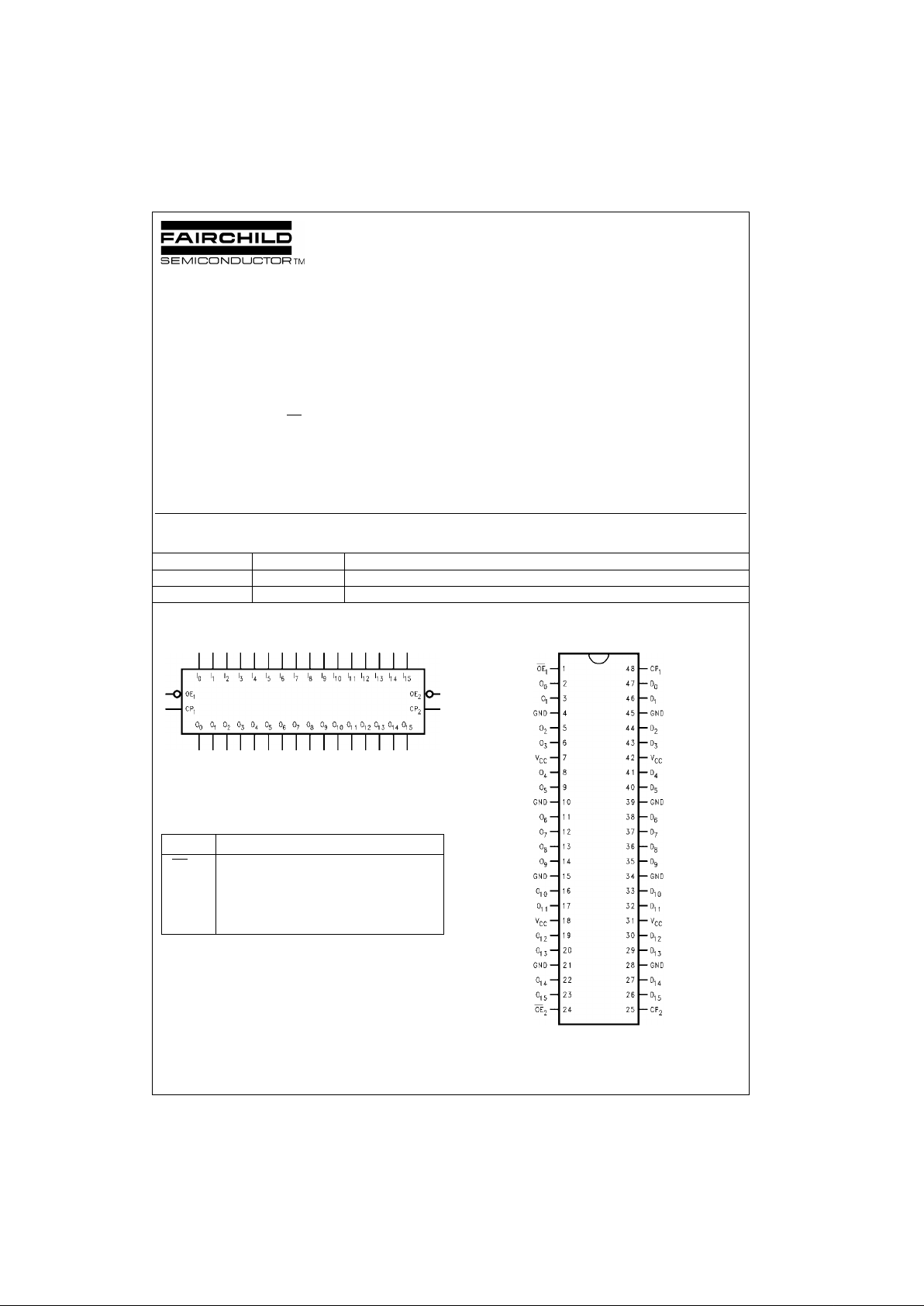
Logic Symbol
Pin Descriptions
Connection Diagram
Order Number Package Number Package Description
74ABT16374CSSC MS48A 48-Lead Small Shrink Outline Package (SSOP), JEDEC MO-118, 0.300” Wide
74ABT16374CMTD MTD48 48-Lead Thin Shrink Small Outline Package (TSSOP), JEDEC MO-153, 6.1mm Wide
Pin Name Description
OE
n
3-STATE Output Enable Input (Active LOW)
CP
n
Clock Pulse Input (Active Rising Edge)
D
0–D15
Data Inputs
O
0–O15
3-STATE Outputs
Page 2
www.fairchildsemi.com 2
74ABT16374
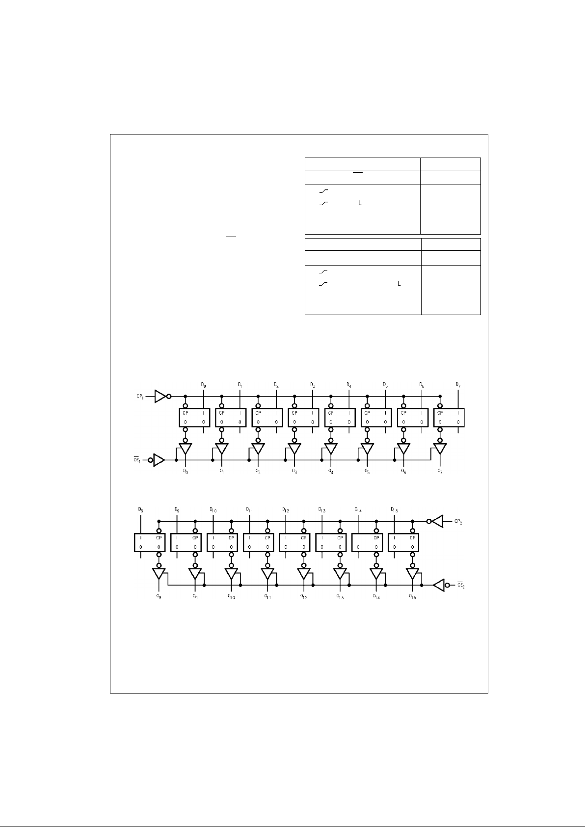
Functional Description
The ABT16374 consists o f si xte en edg e-t rigg er ed f lip -flo ps
with individual D-type inputs and 3-STATE true outputs.
The device is byte controlled with each byte functionin g
identically, but independent of the ot her. The control pins
can be shorted together to obtain full 16-bit operation.
Each byte has a buffered clock and buffered Output Enable
common to all flip-flo ps within that byte. The description
which follows applies to each byte. Each flip-flop will store
the state of their individual D inputs that meet the setup and
hold time requirem ents on the LOW-to-HIG H Clock (CP
n
)
transition. With the Output Ena ble (OE
n
) LOW, the con-
tents of the flip-flops a re available at the outputs. When
OE
n
is HIGH, the outputs go to the high imped ance state.
Operation of the OE
n
input does not affect the st ate of the
flip-flops.
Tr uth Tables
H = HIGH Voltage Level
L = LOW Voltage Level
X = Immaterial
Z = High Impedance
Logic Diagrams
Byte 1 (0:7)
Byte 2 (8:15)
Inputs Outputs
CP
1
OE
1
D0–D
7
O0–O
7
L H H
L L L
L L X (Previous)
X H X Z
Inputs Outputs
CP
2
OE
2
D8–D
15
O8–O
15
L H H
L L L
L L X (Previous)
X H X Z
Page 3

3 www.fairchildsemi.com
74ABT16374
Absolute Maximum Ratings(Note 1) Recommended Operating
Conditions
Note 1: Absolute maximum ratings are values beyond which the device
may be damaged or have its useful life impaired . Functional operation
under these conditions is not implied.
Note 2: Either voltage lim it or c urrent limit is sufficient to protect inputs.
DC Electrical Characteristics
Note 3: Guaranteed, but not tested.
Note 4: For 8-bit toggling, I
CCD
< 0.8 mA/MHz.
Storage Temperature −65°C to +150°C
Ambient Temperature under Bias −55°C to +125°C
Junction Temperature under Bias −55°C to +150°C
V
CC
Pin Potential to Ground Pin −0.5V to +7.0V
Input Voltage (Note 2) −0.5V to +7.0V
Input Current (Note 2) −30 mA to +5.0 mA
Voltage Applied to Any Output
in the Disabled or
Power-Off State −0.5V to 5.5V
in the HIGH State −0.5V to V
CC
Current Applied to Output
in LOW State (Max) twice the rated I
OL
(mA)
DC Latchup Source Current:
OE
Pin −350 mA
(Across Comm Operating Range)
Other Pins −500 mA
Over Voltage Latchup (I/O)
10V
Free Air Ambient Temperature −40°C to +85°C
Supply Voltage +4.5V to +5.5V
Minimum Input Edge Rate (∆V/∆t)
Data Input 50 mV/ns
Enable Input 20 mV/ns
Clock Input 100mV/ns
Symbol Parameter Min Typ Max Units
V
CC
Conditions
V
IH
Input HIGH Voltage 2.0 V Recognized HIGH Signal
V
IL
Input LOW Voltage 0.8 V Recognized LOW Signal
V
CD
Input Clamp Diode Voltage −1.2 V Min IIN = −18 mA
V
OH
Output HIGH Voltage 2.5 V Min IOH = −3 mA
2.0 V Min IOH = −32 mA
V
OL
Output LOW Voltage 0.55 V Min IOL = 64 mA
I
IH
Input HIGH Current 1
µAMax
VIN = 2.7V (Note 3)
1V
IN
= V
CC
I
BVI
Input HIGH Current Breakdown Test 7 µAMaxVIN = 7.0V
I
IL
Input LOW Current −1
µAMax
VIN = 0.5V (Note 3)
−1V
IN
= 0.0V
V
ID
Input Leakage Test 4.75 V 0.0 IID = 1.9 µA
All Other Pins Grounded
I
OZH
Output Leakage Current 10 µA0−5.5V
V
OUT
= 2.7V; OE = 2.0V
I
OZL
Output Leakage Current −10 µA0−5.5V
V
OUT
= 0.5V; OE = 2.0V
I
OS
Output Short-Circuit Current −100 −275 mA Max V
OUT
= 0.0V
I
CEX
Output HIGH Leakage Current 50 µAMaxV
OUT
= V
CC
I
ZZ
Bus Drainage Test 100 µA0.0V
OUT
= 5.5V; All Others VCC or GND
I
CCH
Power Supply Current 2.0 mA Max All Outputs HIGH
I
CCL
Power Supply Current 62 mA Max All Outputs LOW
I
CCZ
Power Supply Current 2.0 mA Max
OE = VCC; All Others at VCC or GND
I
CCT
Additional ICC/Input Outputs Enabled 2.5 mA VI = VCC − 2.1V
Outputs 3-STATE 2.5 mA Max Enable Input VI = VCC − 2.1V
Outputs 3-STATE 2.5 mA Data Input VI = VCC − 2.1V
All Others at VCCor GND
I
CCD
Dynamic I
CC
No Load mA/
Max
Outputs Open
(Note 3) 0.30
MHz
OE = GND, (Note 4)
One Bit Toggling, 50% Duty Cycle
Page 4

www.fairchildsemi.com 4
74ABT16374
AC Electrical Characteristics
(SSOP Package)
AC Operating Requirements
Capacitance
Note 5: C
OUT
is measured at frequency f = 1 MHz, per MIL-STD-883, Method 3012.
Symbol Parameter
TA = +25°CT
A
= −40°C to +85°C
Units
V
CC
= +5.0V VCC = 4.5V to 5.5V
CL = 50 pF CL = 50 pF
Min Typ Max Min Max
f
MAX
Maximum Clock Frequency 150 150 MHz
t
PLH
Propagation Delay 1.8 6.2 1.8 6.2
ns
t
PHL
CP to O
n
1.8 5.9 1.8 5.9
t
PZH
Output Enable Time 1.2 5.6 1.2 5.6
ns
t
PZL
1.6 5.3 1.6 5.3
t
PHZ
Output Disable Time 2.2 7.1 2.2 7.1
ns
t
PLZ
2.2 6.6 2.2 6.6
Symbol Parameter
TA = +25°CT
A
= −40°C to +85°C
Units
V
CC
= +5.0V VCC = 4.5V to 5.5V
CL = 50 pF CL = 50 pF
Min Max Min Max
tS(H) Setup Time, HIGH 1.1 1.1
ns
tS(L) or LOW Dn to CP 1.1 1.1
tH(H) Hold Time, HIGH 1.3 1.3
ns
tH(L) or LOW Dn to CP 1.3 1.3
tW(H) Pulse Width, CP 3.0 3.0
ns
tW(L) HIGH or LOW 3.0 3.0
Symbol Parameter Typ Units
Conditions
(TA = 25°C)
C
IN
Input Capacitance 5.0 pF VCC = 0V
C
OUT
(Note 5) Output Capacitance 11.0 pF VCC = 5.0V
Page 5

5 www.fairchildsemi.com
74ABT16374
Physical Dimensions inches (millimeters) unless otherwise noted
48-Lead Small Shrink Outline Package (SSOP), JEDEC MO-118, 0.300” Wide
Package Num b er MS48A
Page 6

www.fairchildsemi.com 6
74ABT16374 16-Bit D-Type Flip-Flop with 3-STATE Outputs
Physical Dimensions inches (millimeters) unless otherwise noted (Continued)
48-Lead Thin Shrink Small Outline Package (TSSOP), JEDEC MO-153, 6.1mm Wide
Package Number MTD48
Fairchild does not assume any responsibility for use of any circuitr y described, no circuit patent licenses are implied and
Fairchild reserves the right at any time without notice to change said circuitry and specifications.
LIFE SUPPORT POLICY
FAIRCHILD’S PRODUCTS ARE NOT AUTHORIZED FOR USE AS CRITICAL COMPONENTS IN LIFE SUPPORT
DEVICES OR SYSTEMS WITHOUT THE EXPRESS WRITTEN APPROVAL OF THE PRESIDENT OF FAIRCHILD
SEMICONDUCTOR CORPORATION. As used herein:
1. Life support devices or systems are devices or syste ms
which, (a) are intended for surgical implant into the
body, or (b) support or sustain life, and (c) whose failure
to perform when properly used in accordance with
instructions for use provided in the labeling, can be reasonably expected to result in a significant inju ry to the
user.
2. A critical com ponent in any compon ent of a l ife supp ort
device or system whose failure t o perform can be reasonably expected to ca use the failure of the life supp ort
device or system, or to affect its safety or effectiveness.
www.fairchildsemi.com
 Loading...