

Datasheet 7025ERPQS45, 7025ERPQS35, 7025ERPQI45, 7025ERPQI35, 7025ERPQE45 Datasheet (MAXWELL)
...Page 1
1
Memory
All data sheets are subject to change without notice
(619) 503-3300- Fax: (619) 503-3301- www.maxwell.com
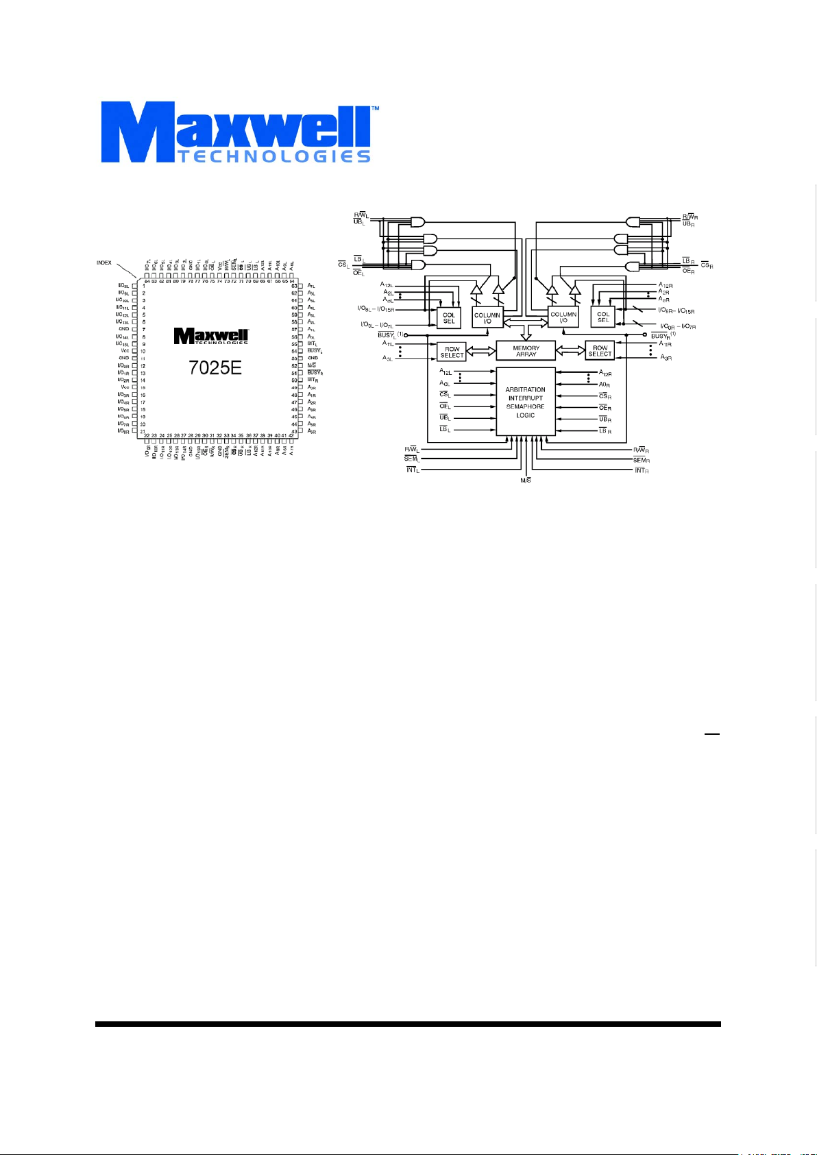
(8K x 16-Bit) Dual Port RAM
7025E
©2001 Maxwell Technologies
All rights reserved.
High-Speed CMOS
12.19.01 Rev 2
1000586
FEATURES:
• 8K x 16-bit dual port RAM
- Stand Alone
- Master Slave
•R
AD-PAK® radiation-hardened against natural space
radiation
• Total dose hardness:
- > 100 krad (Si), depending upon space mission
• Excellent Single Event Effects:
-SEL
TH
LET = >100 MeV/mg/cm
2
-SEUTH LET = 7 MeV/mg/cm
2
• Package:
-84 Pin R
AD-PAK® quad flat pack
• Separate upper byte and lower byte control for multiplexed
bus compatibility
• High speed access time: 35/45 ns
• Expandable to 32 bits or more using master/slave select
when cascading
• High speed CMOS technology
-TTL compatible, single 5V power supply
-Interrupt flag for port-to-port communication
-On chip port arbitration logic
-Asynchronous operation from either port
DESCRIPTION:
Maxwell Technologies’ 7025E Dual Port RAM High Speed
CMOS® microcircuit features a greater than 100 krad (Si) total
dose tolerance, depending upon space mission. The 7025E is
designed to be used as a stand-alone 128k-bit Dual Port RAM
or as a combination MASTER/SLAVE Dual-Port RAM for 32bit or more word systems. This design results in full-speed,
error-free operation without the need for additional discrete
logic. The 7025E provides two independent ports with separate control, address, and I/O pins that permit independent,
asynchronous access for reads or writes to any location in
memory. An automatic power down feature controlled by CS
permits the on-chip circuitry of each port to enter a very low
standby power mode.
Maxwell Technologies' patented R
AD-PAK® packaging technol-
ogy incorporates radiation shielding in the microcircuit package. It eliminates the need for box shielding while providing
the required radiation shielding for a lifetime in orbit or space
mission. In a GEO orbit, R
AD-PAK provides greater than 100
krad (Si) radiation dose tolerance. This product is available
with screening up to Class S.
Logic Diagram
Page 2
Memory
2
All data sheets are subject to change without notice
©2001 Maxwell Technologies
All rights reserved.
(8K x 16-Bit) Dual Port RAM High-Speed CMOS
7025E
12.19.01 Rev 2
1000586
TABLE 1. 7025E PINOUT DESCRIPTION
NAMES LEFT PORT RIGHT PORT
Chip Select CS
L
CS
R
Read/Write Select R/W
L
R/W
R
Output Select OS
L
OS
R
Address AOL-A12
L
AOR-A12
R
Data Input/Output I/OOL-I/O15
L
I/OOR-I/O15
R
Semaphore Select SEM
L
SEM
R
Upper Byte Select UB
L
UB
R
Lower Byte Select LB
L
LB
R
Interrupt Flag INT
L
INT
R
Busy Flag BUSY
L
BUSY
R
M/S Master or Slave Select
V
CC
Power
GND Ground
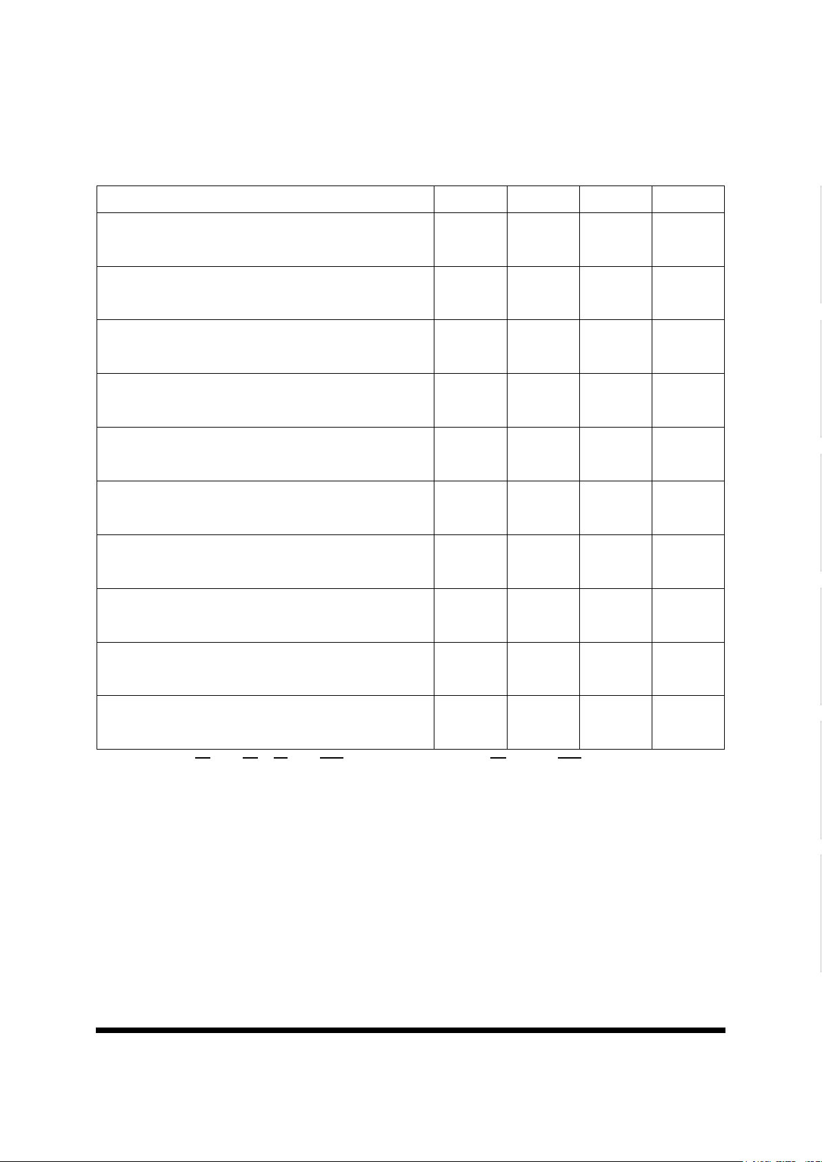
TABLE 2. 7025E ABSOLUTE MAXIMUM RATINGS
PARAMETER SYMBOL MIN MAX UNITS
Supply Voltage (Relative to VSS)V
CC
-0.3 7.0 V
Operating Temperature Range T
A
-55 125
°
C
Input or Output Voltage Applied -- GND -0.3V V
CC
+ 0.3 V
Storage Temperature Range T
STG
-65 150
°
C
TABLE 3. 7025E RECOMMENDED OPERATING CONDITIONS
PARAMETER SYMBOL MIN MAX UNITS
Supply Voltage Positive V
CC
4.5 5.5 V
Input Voltage V
IL
V
IH
-0.5
2.2
0.8
6.0
V
Thermal Impedance
Θ
JC
-- 1.02 °C/W
Operating Temperature Range T
A
-55 125
°
C
Page 3
Memory
3
All data sheets are subject to change without notice
©2001 Maxwell Technologies
All rights reserved.
(8K x 16-Bit) Dual Port RAM High-Speed CMOS
7025E
12.19.01 Rev 2
1000586
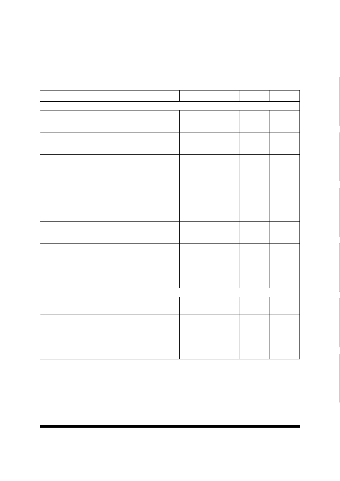
TABLE 4. 7025E CAPACITANCE
PARAMETER SYMBOL MIN MAX UNITS
Input Capacitance: VIN = 0V
1
1. Guaranteed by design.
C
IN
-- 5 pF
Output Capacitance: V
OUT
= 0V
1
C
OUT
-- 7 pF
TABLE 5. 7025E DC ELECTRICAL CHARACTERISTICS
(VCC = 5V ± 10%, TA = -55 TO 125 °C UNLESS OTHERWISE)
P
ARAMETER SYMBOL MIN MAX UNITS
Input Leakage Current
1
1. VCC = 5.5V, VIN = GND to VCC, CS = VIH, VOUT = 0 to VCC.
I
LI
-- ±10 µA
Output Leakage Current
2
2. VIH max = VCC + 0.3V, VIL min = -0.3V or -1V pulse width 50 ns.
I
LO
-- ±10 µA
Standby Supply Current, Both ports TTL level inputs
-35
-45
I
CCSB
--
--
50
50
mA
Standby Supply Current, Both ports CMOS level inputs
-35
-45
I
CCSB1
--
--
5000
5000
µA
Operating Supply Current, Both ports Active
-35
-45
I
CCOP
--
--
320
280
mA
Operating Supply Current, One Port Active, One Port Standby
-35
-45
I
CCOP1
--
--
190
180
mA
Input Low Voltage
Input High Voltage
V
IL
V
IH
--
2.2
0.8
--
V
Output Low Voltage
3
Output High Voltage
3. V
CC
min, IOL = 4 mA, IOH = -4 mA.
V
OL
V
OH
--
2.4
0.4
--
V
TABLE 6. 7025E AC ELECTRICAL CHARACTERISTICS FOR READ CYCLE
(VCC = 5V ± 10%, VSS = 0V, TA = -55 TO 125 °C)
P
ARAMETER SYMBOL MIN MAX UNIT
Read Cycle Time
-35
-45
t
RC
35
45
--
--
ns
Page 4
Memory
4
All data sheets are subject to change without notice
©2001 Maxwell Technologies
All rights reserved.
(8K x 16-Bit) Dual Port RAM High-Speed CMOS
7025E
12.19.01 Rev 2
1000586
Address Access Time
-35
-45
t
AA
--
--
35
45
ns
Chip Select Access Time
1
-35
-45
t
ACS
--
--
35
45
ns
Byte Select Access Time
1
-35
-45
t
ABE
--
--
35
45
ns
Output Select to Output Valid
-35
-45
t
AOE
--
--
20
25
ns
Output Low Z Time
2,3
-35
-45
t
LZ
3
3
--
--
ns
Output High Z Time
2,3
-35
-45
t
HZ
--
--
20
20
ns
Chip Enable to Power Up Time
2
t
PU
0--ns
Chip Disable to Power Up Time
2
t
PD
-- 50 ns
Semaphore Flag Update Pulse (OE
or SEM)t
SOP
15 -- ns
1. To access RAM, CS
= VIL, UB or LB = VIL, SEM = VIH. To access semaphore, CS = VIN and SEM = VIL. Either condition must
be valid for the entire t
EW
time.
2. Guaranteed by design.
3. Transition is measured ± 500 mV from low or high impedance voltage with load.
TABLE 7. 7025E AC ELECTRICAL CHARACTERISTICS FOR WRITE CYCLE
(VCC = 5V ± 10%, VSS = 0V, TA = -55 TO 125 °C)
P
ARAMETER SYMBOL MIN MAX UNIT
Write Cycle Time
-35
-45
t
WC
35
45
--
--
ns
Address Valid to End of Write
-35
-45
t
AW
30
40
--
--
ns
Chip Select to End of Write
1
-35
-45
t
SW
30
40
--
--
ns
TABLE 6. 7025E AC ELECTRICAL CHARACTERISTICS FOR READ CYCLE
(VCC = 5V ± 10%, VSS = 0V, TA = -55 TO 125 °C)
P
ARAMETER SYMBOL MIN MAX UNIT
Page 5
Memory
5
All data sheets are subject to change without notice
©2001 Maxwell Technologies
All rights reserved.
(8K x 16-Bit) Dual Port RAM High-Speed CMOS
7025E
12.19.01 Rev 2
1000586
Address Setup Time
-35
-45
t
AS
0
0
--
--
ns
Write Pulse Width
-35
-45
t
WP
30
35
--
--
ns
Write Recovery Time
-35
-45
t
WR
0
0
--
--
ns
Data Valid to End of Write
-35
-45
t
DW
25
25
--
--
ns
Output High Z Time
2,3
-35
-45
t
HZ
--
--
20
20
ns
Data Hold Time
-35
-45
t
DH
0
0
--
--
ns
Write Select to Output in High Z
2,3
-35
-45
t
WZ
--
--
20
20
ns
Output Active from End of Write
2,3,4
-35
-45
t
OW
0
0
--
--
ns
SEM Flag Write to Read Time
-35
-45
t
SWRD
10
10
--
--
ns
SEM Flag Contention Window
-35
-45
t
SPS
10
10
--
--
ns
1. To access RAM, CS
= VIL, UB or LB = VIL, SEM = VIH. To access semaphore, CS = VIN and SEM = VIL. Either condition must
be valid for the entire t
EW
time.
2. Guaranteed by design.
3. Transition is measured ± 500 mV from low or high impedance voltage with load.
4. The specification for t
DH
must be met by the device supplying write data to the RAM under all operating conditions. Although
t
DH
and tDW.
TABLE 7. 7025E AC ELECTRICAL CHARACTERISTICS FOR WRITE CYCLE
(VCC = 5V ± 10%, VSS = 0V, TA = -55 TO 125 °C)
P
ARAMETER SYMBOL MIN MAX UNIT
Page 6
Memory
6
All data sheets are subject to change without notice
©2001 Maxwell Technologies
All rights reserved.
(8K x 16-Bit) Dual Port RAM High-Speed CMOS
7025E
12.19.01 Rev 2
1000586
TABLE 8. 7025E AC ELECTRICAL CHARACTERISTICS FOR WRITE MASTER/SLAVE CONFIGURATION
(VCC = 5V ± 10%, VSS = 0V, TA = -55 TO 125 °C)
P
ARAMETER SYMBOL MIN MAX UNIT
For Master Only
BUSY Access Time to Address Match
-35
-45
t
BAA
--
--
35
35
ns
BUSY Disable Time to Address Not Matched
-35
-45
t
BDA
--
--
30
30
ns
BUSY Access Time to Chip Select Low
-35
-45
t
BAC
--
--
30
30
ns
BUSY Disable Time to Chip Select High
-35
-45
t
BDC
--
--
25
25
ns
Write Pulse to Data Delay
1
-35
-45
1. Port to port timing delay through RAM cells from writing port to reading port.
t
WDD
--
--
60
70
ns
Write Data Valid to Read Data Delay
1
-35
-45
t
DDD
--
--
45
55
ns
Arbitration Priority Setup Time
2
-35
-45
2. To ensure that the earlier of the two ports wins.
t
APS
5
5
--
--
ns
BUSY Disable to Valid Data
-35
-45
t
BDD
--
--
3
3
3. t
BDD
is a calculated parameter and is the greater of 0, t
WDD
- tWP (actual) or t
DDD
- tWD (actual).
ns
For Slave Only
Write to BUSY Input
4
4. To ensure that the write cycle is inhibited during contention.
t
WB
0--ns
Write Hold after BUSY
5
5. To ensure that a write cycle is completed after contention.
t
WH
25 -- ns
Write Pulse to Data Delay
1
-35
-45
t
WDD
--
--
60
70
ns
Write Data Valid to Read Data Delay
1
-35
-45
t
DDD
--
--
45
55
ns
Page 7

Memory
7
All data sheets are subject to change without notice
©2001 Maxwell Technologies
All rights reserved.
(8K x 16-Bit) Dual Port RAM High-Speed CMOS
7025E
12.19.01 Rev 2
1000586
TABLE 9. 7025E AC PARAMETERS FOR INTERRUPT TIMING
(VCC = 5V ± 10%, TA = -55 TO 125 °C, f = 1 MHZ)
P
ARAMETER SYMBOL MIN MAX UNITS
Address Setup Time t
AS
0--ns
Write Recovery Time t
WR
0--ns
Interrupt Set Time
-35
-45
t
INS
--
--
30
35
ns
Interrupt Reset Time
-35
-45
t
INR
--
--
30
35
ns
TABLE 10. 7025E TRUTH TABLE FOR INTERRUPT FLAG CONTROL
1
1. Assumes BUSYL = BUSYR = H.
F
UNCTION R/W CS OS
A0-A
12
INT
Left Port
Set right INT
L
flag L L X 1FFF X
Reset right INT
L
flag XXXXX
Set left INT
L
flag XXXXL
2
2. If BUSYR = L, then no change.
Reset left INT
L
flag X L L 1FFE H
3
3. If BUSYL = L, then no change.
Right Port
Set right INT
R
flag XXXXL
3
Reset right INTR flag X L L 1FFF H
2
Set left INTR flag L L X 1FFE X
Reset left INT
R
flag XXXXX
Page 8

Memory
8
All data sheets are subject to change without notice
©2001 Maxwell Technologies
All rights reserved.
(8K x 16-Bit) Dual Port RAM High-Speed CMOS
7025E
12.19.01 Rev 2
1000586
TABLE 11. 7025E TRUTH TABLE FOR ARBITRATION OPTIONS
OPTIONS INPUTS OUTPUTS
CS UB LB M/S SEM BUSY INT
Busy Logic Master L
L
X
L
L
X
H
H
H
H
Output Signal --
Busy Logic Slave L
L
X
L
L
X
L
L
H
H
Input Signal --
Interrupt Logic L
L
X
L
L
X
X
X
H
H
-- Output Signal
Semaphore Logic H
H
X
X
X
X
H
L
L
L
H
HI-Z
--
TABLE 12. 7025E NON-CONTENTION READ/WRITE CONTROL
INPUTS
1
1. AOL - A12L ¼ AOR-A12R.
O
UTPUTS
MODE
CS R/W OE UB LB SEM I/O8-I/O15 I/O0-I/O7
HXXXXHHI-Z HI-ZDeselected power down
X X X H H H HI-Z HI-Z Both bytes deselected:
Power down
L L X L H H DATAIN HI-Z Write to upper byte only
L L X H L H HI-Z DATAIN Write to lower byte only
L L X L L H DATAIN DATAIN Write to both bytes
L H L L H H DATAOUT HI-Z Read upper byte only
L H L H L H HI-Z DATAOUT Read lower byte only
L H L L L H DATAOUT DATAOUT Read both bytes
X X H X X X HI-Z HI-Z Outputs disabled
Page 9

Memory
9
All data sheets are subject to change without notice
©2001 Maxwell Technologies
All rights reserved.
(8K x 16-Bit) Dual Port RAM High-Speed CMOS
7025E
12.19.01 Rev 2
1000586
TABLE 13. 7025E SEMAPHORE READ/WRITE CONTROL
1
1. AOL - A12L ¼ AOR-A12R.
I
NPUTS OUTPUTS MODE
CS R/W OE UB LB SEM I/O8-I/O15 I/O0-I/O7
H H L X X L DATAOUT DATAOUT Read data in semaphore
flag
X H L H H L DATAOUT DATAOUT Read data in semaphore
flag
H X X X L DATAIN DATAIN Write DinO into semaphore
flagf
X X H H L DATAIN DATAIN Write DinO into semaphore
flag
LXXLXL -- --Not allowed
L X X X L L -- -- Not allowed
Page 10

Memory
10
All data sheets are subject to change without notice
©2001 Maxwell Technologies
All rights reserved.
(8K x 16-Bit) Dual Port RAM High-Speed CMOS
7025E
12.19.01 Rev 2
1000586
FIGURE 1. TIMING WAVEFORM OF READ CYCLE NO. 1, EITHER SIDE
1,2,3
FIGURE 2. TIMING WAVEFORM OF READ CYCLE NO. 2, EITHER SIDE
1,4,5
1. F/W is high for read cycles.
2. Device is continuously enabled, CS
= VIL, UB or LB = VL. This waveform cannot be used for semaphore reads.
3. CE
= VIL.
4. Addresses valid prior to or coincident with CS
transition.
5. To access RAM, CS
= VL, UB or LB = VIL, SEM = VIH. To access semaphore, CS = VIH, SEM = VIL.
Page 11

Memory
11
All data sheets are subject to change without notice
©2001 Maxwell Technologies
All rights reserved.
(8K x 16-Bit) Dual Port RAM High-Speed CMOS
7025E
12.19.01 Rev 2
1000586
FIGURE 3. TIMING WAVEFORM OF READ CYCLE NO. 3, EITHER SIDE
1,3,4,5
FIGURE 4. TIMING WAVEFORM OF READ WITH BUSY
2,3,4
(FOR MASTER)
1. To ensure math, the earlier of the two ports wins.
2. Write cycle parameters should be adhered to, to ensure proper writing.
3. Device is continuously enable for both ports.
4. OE
= L for the reading port.
Page 12

Memory
12
All data sheets are subject to change without notice
©2001 Maxwell Technologies
All rights reserved.
(8K x 16-Bit) Dual Port RAM High-Speed CMOS
7025E
12.19.01 Rev 2
1000586
FIGURE 5. TIMING WAVEFORM OF WRITE WITH PORT-TO-PORT
1,2,3
(FOR SLAVE ONLY)
1. Assume BUSY Input = H or the writing port, and OE = L for the reading port.
2. Write cycle parameters should be adhered to, to ensure proper writing.
3. Device is continuously enable for both ports.
FIGURE 6. TIMING WAVEFORM OF WRITE CYCLE NO. 1, R/W CONTROLLED TIMING
1,2,3,7
Page 13

Memory
13
All data sheets are subject to change without notice
©2001 Maxwell Technologies
All rights reserved.
(8K x 16-Bit) Dual Port RAM High-Speed CMOS
7025E
12.19.01 Rev 2
1000586
FIGURE 7. TIMING WAVEFORM OF WRITE CYCLE NO. 2, CS CONTROLLED TIMING
1,2,3,5
FIGURE 8. TIMING WAVEFORM OF WRITE WITH BUSY (FOR SLAVE)
1. R/W must be high during all address transitions.
2. A write occurs during the overlap (t
SW
to tWF) of a low CS or SEM and a low R/W.
3. T.
WF
is measured from the earlier of CS or R/W (or SEM or R/W) going high to the end of write cycle.
4. During this period, the I/O pins are in the output state, and input signals must not be applied.
5. If the CS
or SEM low transition occurs simultaneously with or after the R/W low transition, the outputs remain in the
high impedance state.
6. Transitions measured = 500 mV from steady state with a 5 pF load (including scope and jig). This parameter is sample and not 100% tested.
7. If OE
is low during a R/W controlled write cycle, the write pulse width must be the larger of two or (tWZ +tDW) to allow
the I/O driver to turn off and data to be placed on the bus for the required t
DW
. If OE is high during an R/W controlled
write cycle, this requirement does not apply and the write pulse can be as short as the specified t
WP
.
8. To access RAM, CS
= VIL, SEM = VIH.
9. To access upper byte, CS
= VIL, UB = VIL, SEM = VIH.
To access lower byte, CS
= VIL, LB = VIL, SEM = VIH.
Page 14

Memory
14
All data sheets are subject to change without notice
©2001 Maxwell Technologies
All rights reserved.
(8K x 16-Bit) Dual Port RAM High-Speed CMOS
7025E
12.19.01 Rev 2
1000586
FIGURE 9. TIMING WAVEFORM OF CONTENTION CYCLE NO. 1, CS ARBITRATION (FOR MASTER)
F
IGURE 10. TIMING WAVEFORM OF CONTENTION CYCLE NO. 2, ADDRESS VALID ARBITRATION (FOR MASTER
ONLY)
1
LEFT ADDRESS VALID FIRST
Page 15

Memory
15
All data sheets are subject to change without notice
©2001 Maxwell Technologies
All rights reserved.
(8K x 16-Bit) Dual Port RAM High-Speed CMOS
7025E
12.19.01 Rev 2
1000586
RIGHT ADDRESS VALID FIRST
1. CSL = CSR = VIL.
FIGURE 11. WAVEFORM OF INTERRUPT TIMING
1
SET ADDRESS
CLEAR ADDRESS
1. All timing is the same for left and right ports. Port “A” may be either the left or right port. Port “B” is the port opposite
from “A”.
2. See interrupt truth table.
3. Timing depends on which enable signal is asserted last.
4. Timing depends on which enable signal is de-asserted first.
Page 16

Memory
16
All data sheets are subject to change without notice
©2001 Maxwell Technologies
All rights reserved.
(8K x 16-Bit) Dual Port RAM High-Speed CMOS
7025E
12.19.01 Rev 2
1000586
FIGURE 12. 32-BIT MASTER/SLAVE DUAL-PORT MEMORY SYSTEMS
1. No arbitration in Master/Slave. BUSY - IN inhibits write in Master/Slave.
FIGURE 13. TIMING WAVEFORM OF SEMAPHORE READ AFTER WRITE TIMING, EITHER SIDE
1
1. CS = VIH for the duration of the above timing (both write and read cycle).
Page 17

Memory
17
All data sheets are subject to change without notice
©2001 Maxwell Technologies
All rights reserved.
(8K x 16-Bit) Dual Port RAM High-Speed CMOS
7025E
12.19.01 Rev 2
1000586
FIGURE 14. TIMING WAVEFORM OF SEMAPHORE CONTENTION
1,3,4
1. DOR = DOL = VIL, CSR = CSL = VIH, semaphore Flag is released from both sides (reads as ones from both sides) at
cycle start.
2. Either side “A” = left and side “B” = right, or side “A” = right and side “B” = left.
3. This parameter is measured from the point where R/W
A
or SEMA goes high until R/WB or SEMB goes high.
4. If t
SPS
is violated, the semaphore will fall positively to one side or the other, but there is no guaranty which side will
obtain the flag.
Page 18

Memory
18
All data sheets are subject to change without notice
©2001 Maxwell Technologies
All rights reserved.
(8K x 16-Bit) Dual Port RAM High-Speed CMOS
7025E
12.19.01 Rev 2
1000586
Q84-01
Note: All dimensions in inches
84 PIN RAD-PAK® FLAT PACKAGE
SYMBOL DIMENSION
MIN NOM MAX
A 0.163 0.176 0.189
A1 0.113 0.123 0.133
b 0.006 0.010 0.014
c 0.004 0.006 0.010
D 0.635 0.650 0.665
D1 0.500 BSC
e 0.025 BSC
S1 0.005 0.070 --
F1 0.540 0.545 0.550
F2 0.415 0.420 0.425
F3 0.412 0.415 0.418
F4 0.560 0.565 0.570
L -- 1.620 1.635
L1 1.595 1.600 1.615
L2 0.940 0.950 0.960
N84
Page 19

Memory
19
All data sheets are subject to change without notice
©2001 Maxwell Technologies
All rights reserved.
(8K x 16-Bit) Dual Port RAM High-Speed CMOS
7025E
12.19.01 Rev 2
1000586
Important Notice:
These data sheets are created using the chip manufacturers published specifications. Maxwell Technologies verifies
functionality by testing key parameters either by 100% testing, sample testing or characterization.
The specifications presented within these data sheets represent the latest and most accurate information available to
date. However, these specifications are subject to change without notice and Maxwell Technologies assumes no
responsibility for the use of this information.
Maxwell Technologies’ products are not authorized for use as critical components in life support devices or systems
without express written approval from Maxwell Technologies.
Any claim against Maxwell Technologies must be made within 90 days from the date of shipment from Maxwell Technologies. Maxwell Technologies’ liability shall be limited to replacement of defective parts.
Page 20

Memory
20
All data sheets are subject to change without notice
©2001 Maxwell Technologies
All rights reserved.
(8K x 16-Bit) Dual Port RAM High-Speed CMOS
7025E
12.19.01 Rev 2
1000586
Product Ordering Options
Model Number
Feature
Option Details
7025E
RP
Q X
-XX
Access Time
Screening Flow
Package
Radiation Feature
Base Product
Nomenclature
35 = 35 ns
45 = 45 ns
Monolithic
S = Maxwell Class S
B = Maxwell Class B
E = Engineering (testing @ +25°C
)
I = Industrial (testing @ -55°C,
+25°C, +125°C)
Q = Quad Flat Pack
RP = R
AD-PAK® package
(8K x 16-Bit) Dual Port RAM HighSpeed CMOS
 Loading...