

Page 1
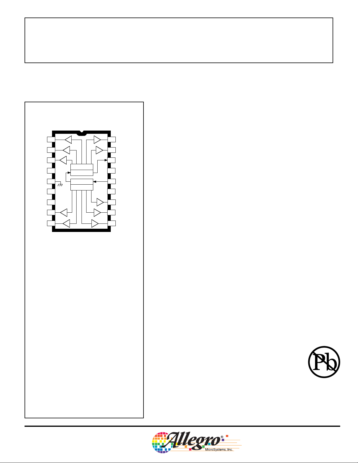
A6810xA
OUT
1
OUT
8
2
OUT
7
3
OUT
CLOCK
GROUND
LOGIC
SUPPLY
STROBE
OUT
OUT
6
CLK
4
5
6
V
7
ST
8
5
4
LATCHES
REGISTER
REGISTER
LATCHES
DD
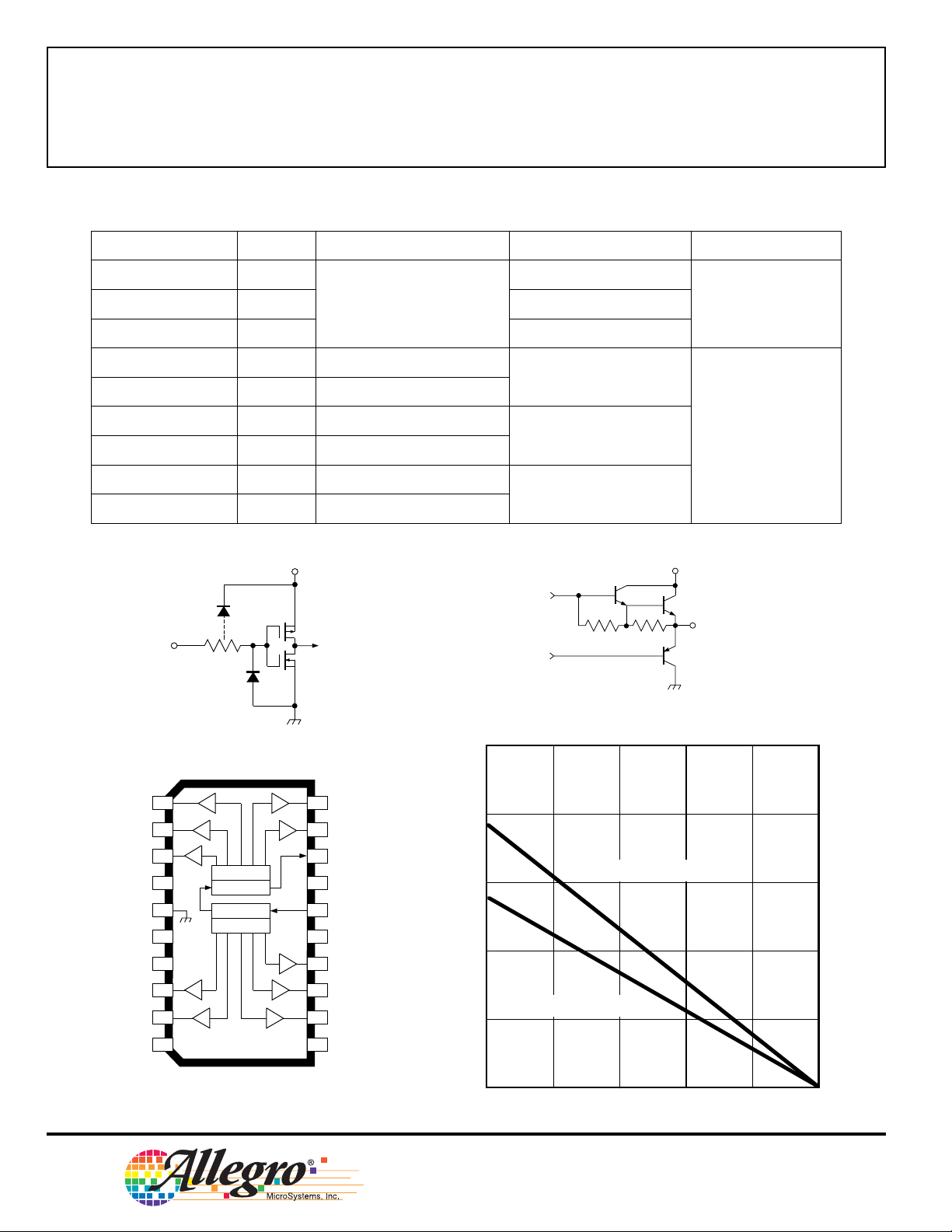
ABSOLUTE MAXIMUM RATINGS
at TA = 25°C
Logic Supply Voltage, V
Driver Supply Voltage, V
Continuous Output Current Range,
I
........................ -40 mA to +15 mA
OUT
Input Voltage Range,
V
....................... -0.3 V to V
IN
Package Power Dissipation,
P
....................................... See Graph
D
Operating Temperature Range, T
(Suffi x ‘E–’) ................... -40°C to +85°C
(Suffi x ‘K–’) ................. -40°C to +125°C
(Suffi x ‘S–’) ................... -20°C to +85°C
Storage Temperature Range,
T
............................... -55°C to +125°C
S
Caution: These CMOS devices have input
static protection (Class 2) but are still susceptible to damage if exposed to extremely
high static electrical charges.
DD
BB
18
9
17
OUT
10
SERIAL
16
DATA OUT
LOAD
V
15
BB
SUPPLY
SERIAL
14
DATA IN
13
12
11
019
BLANKING
OUT
1
OUT
2
OUT
3
Dwg. PP-029
BLNK
.................. 7.0 V
................... 60 V
+ 0.3 V
DD
A
26182.124E
Data Sheet
6810
DABiC-IV, 10-BIT SERIAL-INPUT,
LATCHED SOURCE DRIVER
The A6810– devices combine 10-bit CMOS shift registers, ac com pa ny ing data latches and control cir cuit ry with bipolar sourcing out puts
and pnp active pull downs. De signed pri mar ily to drive vacuum-fl u o -
res cent displays, the 60 V and -40 mA output ratings also allow these
devices to be used in many other peripheral power driver ap pli ca tions.
The A6810– feature an increased data input rate (com pared with the
older UCN/UCQ5810-F) and a con trolled output slew rate.
The CMOS shift register and latches allow direct interfacing with
microprocessor-based systems. With a 3.3 V or 5 V logic supply, serialdata input rates of at least 10 MHz .
A CMOS serial data output permits cascade con nec tions in ap pli ca tions re quir ing additional drive lines. Similar devices are available as
the A6812– (20 bits) and A6818– (32 bits).
The A6810– output source drivers are npn Dar ling tons, capable of
sourcing up to 40 mA. The controlled output slew rate reduces elec tro mag net ic noise, which is an important consideration in systems that include telecommunications and/or microprocessors and to meet government emissions regulations. For inter-digit blanking, all output drivers
can be dis abled and all sink drivers turned on with a BLANK ING input
high. The pnp active pull-downs will sink at least
2.5 mA.
The A6810– are available in three temperature ranges for op ti mum
per for mance in commercial (suffi x S-), industrial (suffi x E-), or au-
tomtoive (suffi x K–) ap pli ca tions. They are provided in two package
styles for through-hole DIP (suffi x -A) or minimum-area surface-mount
SOIC (suffi x -LW). Copper lead frames, low logic-power dis si pa tion,
and low output-saturation voltages allow all devices to source 25 mA
from all outputs continuously over the max i mum operating tem pera ture
range.
The lead (Pb) free versions are provided with 100% matte tin
leadframe plating.
FEATURES
■ Controlled Output Slew Rate
■ High-Speed Data Storage
■ 60 V Minimum Output Breakdown
■ High Data Input Rate
■ PNP Active Pull-Downs
■ Low Output-Saturation Voltages
■ Low-Power CMOS Logic and Latches
■ Improved Replacements for TL4810–, UCN5810–, and UCQ5810–
Page 2
6810
10-BIT SERIAL-INPUT,
LATCHED SOURCE DRIVER
PRODUCT SELECTION GUIDE
Part Number Pb-free Packing
A6810SA
A6810SA-T
A6810EA
A6810EA-T
A6810KA
A6810KA-T
A6810SLW
A6810SLW-T
A6810SLWTR
A6810SLWTR-T
A6810ELW
A6810ELW-T
A6810ELWTR
A6810ELWTR-T
A6810KLW
A6810KLW-T
A6810KLWTR
A6810KLWTR-T
Yes
Yes
Yes
Yes
Yes
Yes
Yes
Yes
Yes
–
–
–
–
–
1000 pieces/13-in. reel
–
–
1000 pieces/13-in. reel
–
–
1000 pieces/13-in. reel
TIUCRICTUPNILACIPYT
V
DD
IN
21 pieces/tube
37 pieces/tube
37 pieces/tube
37 pieces/tube
Ambient Temperature, T
(°C)
–20 to 85
–40 to 85
–40 to 125
–20 to 85
–40 to 85
–40 to 125
Dwg. EP-021-19
A
Package
18-pin DIP
20-pin SOIC-W
REVIRDTUPTUOLACIPYT
V
BB
OUT
N
OUT
OUT
OUT
CLOCK
GROUND
LOGIC SUPPLY
STROBE
OUT
OUT
CONNECTION
NO
Dwg. EP-010-5
A6810xLW
1
8
2
7
3
6
4
5
6
7
8
5
9
4
10
CLK
V
ST
NC
LATCHES
REGISTER
REGISTER
LATCHES
DD
V
BLNK
NC
BB
20
OUT
19
OUT
SERIAL
18
DATA OUT
17
LOAD SUPPLY
SERIAL
16
DATA IN
15
BLANKING
14
OUT
13
OUT
12
OUT
NO
11
CONNECTION
9
10
1
2
3
Dwg. PP-029-2
2.5
2.0
SUFFIX 'A', R
QJA
= 65oC/W
1.5
1.0
SUFFIX 'LW', R
QJA
= 90oC/W
0.5
0
25
ALLOWABLE PACKAGE POWER DISSIPATION IN WATTS
50 75 100 125 150
AMBIENT TEMPERATURE IN ooooC
115 Northeast Cutoff, Box 15036
Worcester, Massachusetts 01615-0036 (508) 853-5000
Copyright © 1998, 2003 Allegro MicroSystems, Inc.
Page 3
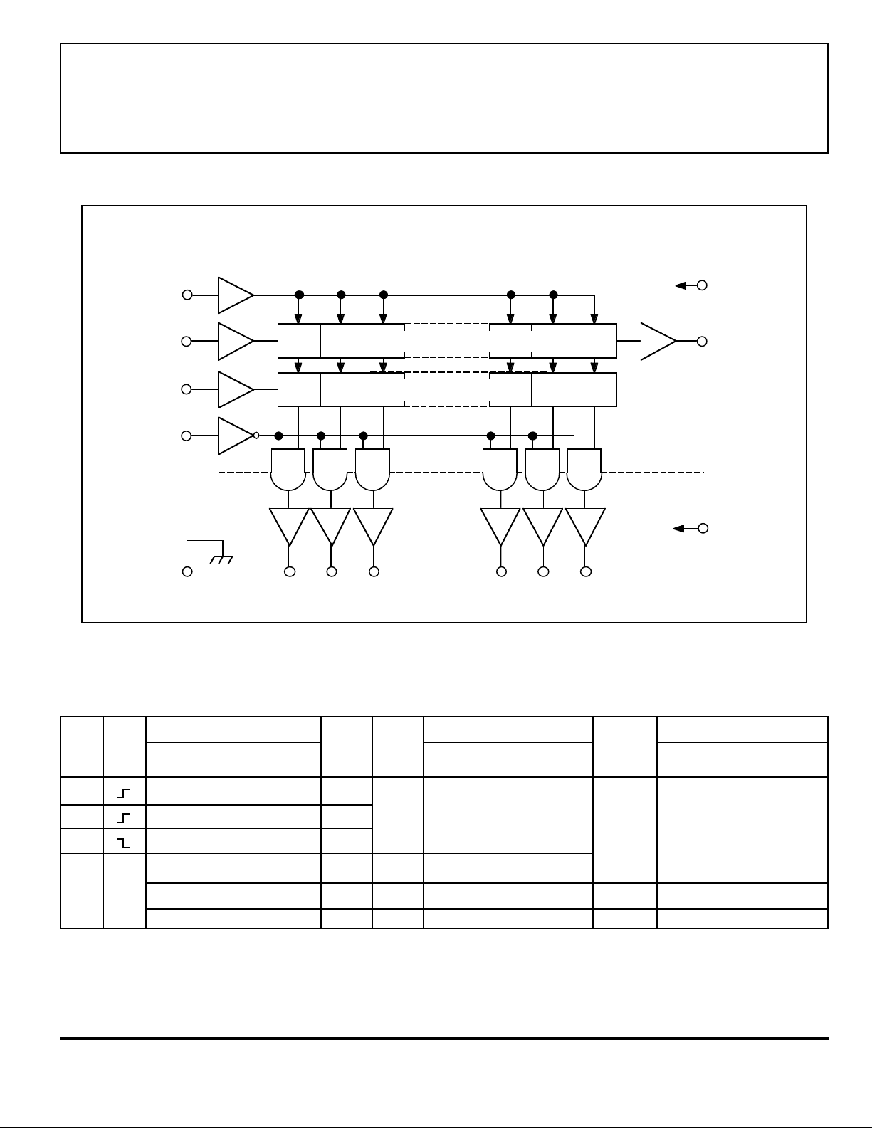
LATCHED SOURCE DRIVER
FUNCTIONAL BLOCK DIAGRAM
6810
10-BIT SERIAL-INPUT,
CLOCK
SERIAL
DATA IN
STROBE
BLANKING
GROUND
OUT1OUT
SERIAL-PARALLEL SHIFT REGISTER
LATCHES
OUT
2
3
OUT
N
V
DD
MOS
BIPOLAR
V
BB
LOGIC
SUPPLY
SERIAL
DATA OUT
LOAD
SUPPLY
Dwg. FP-013-1
TRUTH TABLE
Serial Shift Register Contents Serial Latch Contents Output Contents
Data Clock Data Strobe
Input Input I
1I2I3
HHR
LLR
XR
1R2R3
XXX...X X X L R1R2R3... R
P1P2P3... P
L = Low Logic Level H = High Logic Level X = Irrelevant P = Present State R = Previous State
www.allegromicro.com
1R2
1R2
... I
... R
... R
... R
N-1IN
N-2RN-1
N-2RN-1
N-1RN
N-1PN
Output Input I1I2I3... I
R
N-1
R
N-1
R
N
P
N
HP1P2P3... P
X X X ... X X H L L L ... L L
N-1IN
N-1 RN
N-1 PN
Blanklng I1I2I3... I
LP1P2P3... P
N-1
N-1 PN
I
N
Page 4

6810
10-BIT SERIAL-INPUT,
LATCHED SOURCE DRIVER
ELECTRICAL CHARACTERISTICS at T
= +25°C (A6810S-) or over operating temperature
A
range (A6810E-), VBB = 60 V unless otherwise noted.
Limits @ VDD = 3.3 V Limits @ VDD = 5 V
Characteristic Symbol Test Conditions Mln. Typ. Max. Min. Typ. Max. Units
V
Output Leakage Current I
Output Voltage V
Output Pull-Down Current I
OUT(1)IOUT
V
OUT(0)IOUT
OUT(0)
Input Voltage V
V
Input Current I
I
Input Clamp Voltage V
Serial Data Output Voltage V
OUT(1)IOUT
V
OUT(0)IOUT
Maximum Clock Frequency f
Logic Supply Current I
Load Supply Current I
-to-
Blanking
Strobe
Output Delay t
-to-
Output Delay t
DD(1)
I
DD(0)
BB(1)
I
BB(0)
dis(BQ)
t
en(BQ)
p(STH-QL)RL
t
p(STH-QH)RL
Output Fall Time t
Output Rise Time t
CEX
IN(1)
IN(0)
IN(1)
IN(0)
IK
c
f
r
= 0 V — <-0.1 -15 — <-0.1 -15 µA
OUT
= -25 mA 57.5 58.3 — 57.5 58.3 — V
= 1 mA — 1.0 1.5 — 1.0 1.5 V
V
= 5 V to V
OUT
BB
2.5 5.0 — 2.5 5.0 — mA
2.2 — — 3.3 — — V
— — 1.1 — — 1.7 V
VIN = V
DD
— <0.01 1.0 — <0.01 1.0 µA
VIN = 0 V — <-0.01 -1.0 — <-0.01 -1.0 µA
IIN = -200 µA — -0.8 -1.5 — -0.8 -1.5 V
= -200 µA 2.8 3.05 — 4.5 4.75 — V
= 200 µA — 0.15 0.3 — 0.15 0.3 V
10* — — 10* — — MHz
All Outputs High — 0.25 0.75 — 0.3 1.0 mA
All Outputs Low — 0.25 0.75 — 0.3 1.0 mA
All Outputs High, No Load — 1.5 3.0 — 1.5 3.0 mA
All Outputs Low — 0.2 20 — 0.2 20 µA
CL = 30 pF, 50% to 50% — 0.7 2.0 — 0.7 2.0 µs
CL = 30 pF, 50% to 50% — 1.8 3.0 — 1.8 3.0 µs
= 2.3 kΩ, CL ≤ 30 pF — 0.7 2.0 — 0.7 2.0 µs
= 2.3 kΩ, CL ≤ 30 pF — 1.8 3.0 — 1.8 3.0 µs
RL = 2.3 kΩ, CL ≤ 30 pF 2.4 — 12 2.4 — 12 µs
RL = 2.3 kΩ, CL ≤ 30 pF 2.4 — 12 2.4 — 12 µs
Output Slew Rate dV/dt RL = 2.3 kΩ, CL ≤ 30 pF 4.0 — 20 4.0 — 20 V/µs
Clock
-to-
Serial Data Out Delay t
Negative current is defined as coming out of (sourcing) the specified device terminal.
Typical data is is for design information only and is at TA = +25°C.
*Operation at a clock frequency greater than the specified minimum value is possible but not warranteed.
p(CH-SQX)IOUT
= ±200 µA — 50 — — 50 — ns
115 Northeast Cutoff, Box 15036
Worcester, Massachusetts 01615-0036 (508) 853-5000
Page 5

10-BIT SERIAL-INPUT,
LATCHED SOURCE DRIVER
TIMING REQUIREMENTS and SPECIFICATIONS
(Logic Levels are VDD and Ground)
C
6810
CLOCK
SERIAL
DATA IN
SERIAL
DATA OUT
STROBE
BLANKING
OUT
BLANKING
OUT
50%
A B
DATA
N
N
50%
t
p(CH-SQX)
t
p(STH-QH)
t
p(STH-QL)
10%
DATA
90%
t
dis(BQ)
50%
D E
50%
LOW = ALL OUTPUTS ENABLED
HIGH = ALL OUTPUTS BLANKED (DISABLED)
50%
t
en(BQ)
t
r
DATA
10%
DATA
Dwg. WP-029
t
f
90%
50%
A. Data Active Time Before Clock Pulse
(Data Set-Up Time), t
......................................... 25 ns
su(D)
B. Data Active Time After Clock Pulse
(Data Hold Time), t
C. Clock Pulse Width, t
D. Time Between Clock Activation and Strobe, t
E. Strobe Pulse Width, t
............................................... 25 ns
h(D)
............................................... 50 ns
w(CH)
....... 100 ns
su(C)
............................................. 50 ns
w(STH)
NOTE – Timing is representative of a 10 MHz clock. Higher
speeds may be attainable; operation at high temperatures will
reduce the specified maximum clock frequency.
Serial Data present at the input is transferred to the shift
register on the logic “0” to logic “1” transition of the CLOCK
input pulse. On succeeding CLOCK pulses, the registers shift
data information towards the SERIAL DATA OUTPUT. The
www.allegromicro.com
Dwg. WP-030A
SERIAL DATA must appear at the input prior to the rising edge
of the CLOCK input waveform.
Information present at any register is transferred to the
respective latch when the STROBE is high (serial-to-parallel
conversion). The latches will continue to accept new data as
long as the STROBE is held high. Applications where the
latches are bypassed (STROBE tied high) will require that the
BLANKING input be high during serial data entry.
When the BLANKING input is high, the output source
drivers are disabled (OFF); the pnp active pull-down sink
drivers are ON. The information stored in the latches is not
affected by the BLANKING input. With the BLANKING input
low, the outputs are controlled by the state of their respective
latches.
Page 6

6810
10-BIT SERIAL-INPUT,
LATCHED SOURCE DRIVER
18
0.280
0.240
A6810EA & A6810SA
Dimensions in Inches
(controlling dimensions)
10
0.014
0.008
0.300
BSC
0.430
MAX
0.210
MAX
7.11
6.10
0.015
MIN
18
1
0.070
0.045
0.022
0.014
0.920
0.880
0.100
BSC
9
0.005
MIN
0.150
0.115
Dwg. MA-001-18A in
Dimensions in Millimeters
(for reference only)
0.355
10
1
1.77
1.15
23.37
22.35
2.54
BSC
9
0.13
MIN
0.204
7.62
BSC
10.92
MAX
5.33
MAX
0.39
MIN
0.558
0.356
3.81
2.93
NOTES: 1. Exact body and lead configuration at vendor’s option within limits shown.
2. Lead spacing tolerance is non-cumulative.
3. Lead thickness is measured at seating plane or below.
4. Supplied in standard sticks/tubes of 21 devices.
115 Northeast Cutoff, Box 15036
Worcester, Massachusetts 01615-0036 (508) 853-5000
Dwg. MA-001-18A mm
Page 7

A6810ELW & A6810SLW
Dimensions in Inches
(for reference only)
20 11
6810
10-BIT SERIAL-INPUT,
LATCHED SOURCE DRIVER
0.0125
0.0091
0.2992
0.2914
0.020
0.013
0.0926
0.1043
7.60
7.40
1 2
0.0040
20
MIN.
3
0.5118
0.4961
0.050
Dimensions in Millimeters
(controlling dimensions)
11
BSC
0.419
0.394
0.050
0.016
0° TO 8°
Dwg. MA-008-20 in
0.32
0.23
10.65
10.00
0.51
0.33
2.65
2.35
1
0.10
2
MIN.
3
13.00
12.60
1.27
BSC
NOTES: 1. Exact body and lead configuration at vendor’s option within limits shown.
2. Lead spacing tolerance is non-cumulative.
3. Supplied in standard sticks/tubes of 37 devices or add “TR” to part number for tape and reel.
www.allegromicro.com
1.27
0.40
0° TO 8°
Dwg. MA-008-20 mm
Page 8

6810
10-BIT SERIAL-INPUT,
LATCHED SOURCE DRIVER
The products described here are manufactured under one or more
U.S. patents or U.S. patents pending.
Allegro MicroSystems, Inc. reserves the right to make, from time to
time, such departures from the detail specifications as may be
required to permit improvements in the performance, reliability, or
manufacturability of its products. Before placing an order, the user is
cautioned to verify that the information being relied upon is current.
Allegro products are not authorized for use as critical components
in life-support devices or systems without express written approval.
The information included herein is believed to be accurate and
reliable. However, Allegro MicroSystems, Inc. assumes no responsibility for its use; nor for any infringement of patents or other rights of
third parties which may result from its use.
115 Northeast Cutoff, Box 15036
Worcester, Massachusetts 01615-0036 (508) 853-5000
 Loading...