

Page 1

www.fairchildsemi.com
Application Note 6004
500W Power-Factor-Corrected (PFC) Converter Design with FAN4810
This application note describes the theory of operation and
step-by-step process to design a high performance Power
Factor Corrected (PFC) power supply using the FAN4810
controller IC. A complete application circuit is shown in
Figure 10 and an evaluation board using this design is available from Fairchild Sales. The evaluation board provides
500W at 400VDC and 1.25A, while operating from 90V to
264VAC line input.
Selection of Power Train
Components
The FAN4810 can be used in any active PFC pre-regulator
employing Continuous Conduction Mode (CCM) that has to
comply with the IEC 3000-3-2 standard. This section of the
application note covers calculation parameters and selection
of pre-regulator power train components: boost inductor,
output capacitor and semiconductors.
Selecting the Value of the Boost Inductor
The FAN4810 operates in a continuous conduction code to
minimize peak current and maximize available power. The
value boost inductance found by setting ∆ I, the peak-to- peak
value of high-frequency current, is typically in the area of
20% of the peak value of the maximum line current.
2P
I
_LINE_PK
Where I
_LINE_PK
low line, V
IN
----------------=
V
MIN
(1)
is a peak value of input current occurred at
is RMS value of minimum line voltage, P
MIN
output power and η is efficiency. Value I
value of ∆ I , where dI is the specified percentage rate.
I_L
I_L
is the inductor maximum current.
MAX
∆IdII
×=
_LINE_PK
MAXI_LINE_PK
∆I
------+=
2
Another factor influencing inductor selection is duty cycle D
and switching frequency f
V
2V
–
O
-----------------------------------=
D
MIN
V
O
(4)
.
S
L
P
O
------=
P
IN
η
_LINE_PK
D2V
×
--------------------------------=
f
∆I×
S
(2)
is
O
will define
(3)
MIN
(5)
Selecting the Value of the Bulk Capacitor
A major factor affecting bulk capacitor selection is hold up
time (T
). “Hold-up-time” is a time during which output of
hld
power supply remains in specified range, after interruption of
AC power. Energy J
stored in the bulk capacitor supplies
thd
the down-steam converter during power disruption. Voltage
across bulk capacitor drops during hold-up time, as capacitor
discharges. You should calculate the minimum bus voltage
V
, where output voltage stays in regulation, trans-
O_MIN
former properly resets and components stress are inside the
derating guidelines.
J
THDPOTHLD
×= J
1
---
THD
2
2P
---------------------------------------=
C
THLD××
O
2
V
V
–
O
O_MIN
2
CV
× C– V
O
2
(6)
×()=
O_MIN
2
Setting the Oscillator Frequency
Resistor R6 and capacitor C18 set the oscillator frequency.
Let’s assume a value of C18 = 470 pF. The following equation determines the value of R6
1
--------------------------------------=
R6
C18 0.51× f
×
S
(7)
Selecting Parameters of Gain
Modulator Input Circuits
The FAN4810 Gain Modulator employs three inputs:
1. A current representing a profile of input voltage .
This current is proportional to the instantaneous value
of the input voltage at any given time. This current
programmed by resistor R1, see Fig 1.
2. A voltage proportional to the average value of the
line voltage . To obtain this voltage the input voltage is
filtered and scaled. A two-stage filter consists of resistors R2,R3,R4 and capacitors C2,C3.
3. Output of voltage error amplifier .
REV. 1.0.1 10/31/03
Page 2

AN6004 APPLICATION NOTE
16 1
VEAO
FB
AC
RMS
VEA
–
+
MODULATOR
3.6kΩ
GAIN
V
15
2.5V
I
2
V
4
I
SENSE
3
IEAO
IEA
+
–
3.6kΩ
Figure 1. Gain Modulator and Voltage Error Amplifier
The program resistor for Pin 2 (I
) current input of the
AC
Gain Modulator is based on the following formula:
× G
2V
--------------------------------------------------------------------
≥
R1
Where G
R
is the output resistor of Gain Modulator and
MO
V
GM_OUT_MAX
× RMO×
MIN
V
MAX
MAX
GM_OUT_MAX
is the maximum gain of the Gain Modulator,
is the maximum output voltage of the Gain
Modulator. See the FAN4810 Datasheet for reference.
The voltage divider and necessary filters for providing the
scaled value of average input voltage for the Gain Modulator
Pin 4 (V
) input are shown in Figure 2.
RMS
R2
480
420
360
300
240
180
120
60
VARIABLE GAIN BLOCK CONSTANT (K)
0
0123
VRMS(V)
Figure 3. Gain Modulator Transfer Characteristic
(8)
The voltage at Pin 4 sets V
and must be well-filtered
RMS
and yet able to respond well to transient line voltage
changes. A two-stage RC low pass filter consisting of R2,
R3, R4, C3 and C2 as shown in Figure. 2 is selected to meet
this requirement. The resisitive divider ratio gives an average
DC voltage of 1.1 volts at Pin 4 at minimum line voltage.
2
---
V
AV
2V
=
MIN
π
Va v is the value of average line voltage and V
minimum RMS value of line voltage. Assume R2=R1 and
R3=100k. These values are a common choice for Fairchild
PFC applications.
45
(9)
is the
MIN
R3
R4
C2
C3
Figure 2. Two-Stage Filter Schematic
This resistive divider ratio should provide 1.1V at the lowest
line voltage. The value of 1.1V is chosen based on the
FAN4810 datasheet and Gain Modulator Transfer Characteristic presented in Figure 3. The characteristic curve includes
two segments: the right segment is the area of normal operation conditions with line voltages from 80VAC to 264VAC
and the left segment is the area of brown-out conditions
where the line voltage drops below 80VAC. Maximum gain
occurs at V
V
(V) of 1.1V, corresponding to the maximum gain,
RMS
(V) =1.1V, see curve in Figure 3. The
RMS
defines the criteria selection or resistor divider.
I
RD1
Where V
VAVV
–
--------------------------------------------------=
GM_IN_MAX
R2 R3+
GM_IN_MAX
(10)
=1.1V and I
RD1
V
R4
GM_IN_MAX
--------------------------------=
I
RD1
is the current flowing
(11)
through the divider.
R
TOTAL
C3
C2
R2 R3 R4++=
R
----------------------------------------------------------------=
2 π× f1× R2 R3 R4+()×
1
-------------------------------------------------=
TOTAL
R4 R
×
TOTAL
----------------------------------+
R2 R3 R4+()
2 π× f2× R4×
(12)
(13)
(14)
Two poles circuits presented in Figure 2 has demonstrated
good performance with f
= 15Hz and f
1
= 23Hz.
2
2
REV. 1.0.1 10/31/03
Page 3

APPLICATION NOTE AN6004
Selection Parameters of Current
Sense Circuit
A current sense circuit includes a current sense resistor and a
filter.
Selection of Current Sense Resistor
The voltage drop across the current sense resistor should not
exceed the maximum output voltage of the gain modulator,
whose output is connected to the inverting input of the current error amplifier. See Figure 5. The non-inverting input of
the current error amplifier is connected to the ground and its
inverting input acts as a summing node for summing the
Gain Modulator output with the negative voltage on the
current sense resistor as shown in Figure 4.
V
R5
GM_OUT_MAX
-------------------------------------=
I_L_
MAX
(15)
I_L_
MAXI_LINE_PK
Selection of Current Sense Filter
GND
IAC
VEAO
I
SENSE
3.5K
3.5K
R
filter
100Ω
R5
10
3
C
filter
100nF
Figure 4: Current Sense Amplifier Circuit
The current sense filter is needed to protect the I
from voltage surges at start-up caused by a high inrush
V
–
+
REF
EAO
sense
pin
∆I
------+=
2
current and to enhance Total Harmonic Distortion (THD)
performance when a small boost inductor is used and is
operating in Discontinuous Conduction Mode (DCM) at
light loads.
f_cf
---------------------------------------------=
2 π× R16× C19×
The f_cf filter frequency should be set between f
/6 < f_cf < fS.
f
S
1
and f
S
S
(16)
/6;
R16 = 100 Ω or less is recommended.
Selection Parameters of Current
Error Amplifier Compensation
Network
The FAN4810 employs two control loops for power factor
correction: a current control loop and a voltage control loop.
The current control loop shapes current based on the reference signal from the IAC Pin 2. The voltage loop stabilizes
output voltage and defines THD balance.
The output of the Gain Modulator is a current proportional to
the output of the error amplifier and full sine current IAC on
Pin 2 and is inverse-proportional to the V
4. Output current of the Gain Modulator generates a voltage
on internal resistor RMO (3.6k). This voltage subtracts from
the voltage on sense resistor R5. The difference between the
resulting voltage on the inverting pin of the current error
amplifier and virtual ground on the non-inverting pin generates an output voltage that is applied to the non-inverting
input of comparator. The ramp signal applied to the inverting
input of the comparator controls the output signal on Pin 12.
For example, if the output voltage is decreasing, the output
of the current error amplifier increases the duty cycle.
Increasing the duty cycle will in turn increase the output
voltage, thereby closing the control loop.
voltage on Pin
RMS
VEAO
15
2
4
3
7
V
2.5V
I
AC
V
I
SENSE
RAMP 1
FB
RMS
VEA
–
+
MODULATOR
REV. 1.0.1 10/31/03
16
GAIN
3.6kΩ
3.6kΩ
1
IEAO
IEA
+
-
POWER FACTOR CORRECTOR
0.5V
+
–
OSCILLATOR
TRI-FAULT
+
–
2.75V
-1V
OVP
+
–
+
–
PFC I
LIMIT
V
CC
17V
SRQ
SRQ
13
7.5V
REFERENCE
Q
Q
V
CC
PFC OUT
V
REF
14
12
Figure 5. FAN4810 PFC Block Diagram
3
Page 4
AN6004 APPLICATION NOTE
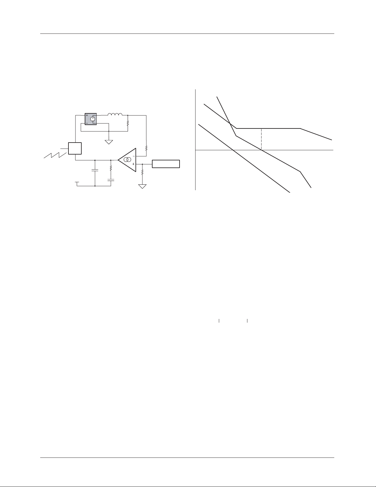
Figure 6 shows a simplified block-diagram of the current
control loop. The PWM block is comprised of a comparator,
flip-flop and output MOSFET driver. The voltage-controlled
voltage source combines input voltage source, rectifier,
MOSFET, and boost diode. The current control loop is
closed around the LR5 pole, essentially eliminating the
inductor from consideration during voltage control loop
analysis.
V_L
D
Ramp
PWM
Vca
C7
Vref
Figure 6. Simplified Diagram of Current Loop
R12
Vs
L
R5
Rmo
Gain Modulator
Rmo
C6
Now determine the transfer function between Vs on the
sense resistor and VCA output of the current amplifier or
transfer function of open loop system. This transfer function
will be a combination of the transfer function of the boost
and PWM blocks of the open loop system.
The duty cycle, voltage applied to the boost inductor, and the
inductor current are determined by the following expressions:
V
------------------=
V
CA
RAMP
V_L D V
×=
O
I_L
D
V_L
--------------=
ω L×
fs. To ensure stability of the converter and fast transient
response, the gain plot of close loop system should intersect
the frequency axis at the crossover frequency (fc_cl) with a
slope of -20 dB/dec. A type two compensation network is
selected. Assume placement of the zero at fcl_z=0.2*fcl and
the placement of the pole at fcl_p=10*fcl.
Gca Gc_c
fcl_z
1k
Hz
fc_
10 k
Hz
Gpwm_boost
cl
100kHz
fcl_
p
Gconverter
Figure 7. Current Control Loop Bode Plots
For the conditions listed above, an open loop system will
have the following gain at crossover frequency.
RAMP
VORS×
2×π× f
RAMP
× L×
C_CL
is the difference between
(17)
G
PWM_BOOST
-------------------------------------------------------------------=
V
The peak-to-peak value of V
the peak voltage and the peak valley values. These parameters are listed in the FAN4810 datasheet.
In Log scale
G
PWM_BOOST_LG
= 20 × log (G
PWM_BOOST
) (18)
Voltage across the sense resistor is given by:
V
V×
V
S
DV×
×
ORS
-------------------------------
ω L×
CA
---------------------------------------==
V
RAMP
O
RS×
ω× L×
Gain of the current error amplifier at crossover frequency is
found from the following expression.
Gpwm_boost_lg
-------------------------------------------
Gc_c 10
= (19)
20
The current loop transfer function is given by the following
expression:
This gain ensures that the closed loop Gain plot will intersect the frequency axe on the Bode plots at unity gain.
V
-----------
V
CA
S
---------------------------------------
V
RAMP
V
ORS
×
ω× L×
V
×
RAMP
ORS
2×π× fS× L×
----------------------------------------------------------==
V
The current error amplifier is the transconductance amplifier,
with the transconductance value of g_ca. Refer to the
FAN4810 Datasheet. The value of R12 can be determined
In this case, the open loop gain of current loop
from following operation:
(GPWM_BOOST)is:
1
(21)
G
PWM_BOOST
----------------------------------------------------------=
V
RAMP
VORS×
2×π× fS× L×
Figure 7 presents the key bode plots of the current control
loop. The bottom curve is the gain of the PWM-boost section
as a function of frequency. The LR pole produces a curve
with a slope of -20 dB/dec. Fairchild recommends a crossover frequency defined as 1/10 of the switching frequency,
R12
C7
Gc_c
------------= (20)
g_ca
------------------------------------------------=
2 π× fcl_p× R12×
1
C6
(22)
------------------------------------------------=
2 π× fcl_z× R12×
The values of C6 and C7 can be found based on the zero and
pole expressions for a type-two compensation network at
frequencies fcl_z and fcl_p.
4 REV. 1.0.1 10/31/03
Page 5
APPLICATION NOTE AN6004
Selection Parameters of Voltage
Error Amplifier Compensation
Network
This section discusses the selection of the voltage divider
and compensation of the voltage error amplifier.
Selection of Resistor Divider
16
VEAO
V
15
2.5V
Figure 8. Resistor Divider
The non-inverting input of the error amplifier connects to a
2.5V reference voltage as shown in Figure 8. Output of the
voltage divider should set at this voltage level. We are
recommending R8=2.37k, in this case a second resistor R8
can be found from following formula.
V
REF
-------------= R7
I
RD2
R8
FB
VEA
–
+
V
–
BUSVREF
----------------------------------=
I
RD2
To prevent increasing the amplitude of third harmonics in the
current waveform and to decrease distortion the bandwidth
of the voltage control loop should be kept in a range from 10
Hz to 30 Hz. Low bandwidth will minimize the appearance
of second harmonics in the input of the current loop and limited THD.
The main reason for using a low-bandwidth voltage control
loop is due to the phase difference between the waveforms of
the input voltage and ripple voltage on the output of PFC, as
shown in Figure 17. The reactive nature of the PFC load
determines the phase difference. If not attenuated, the ripple
voltage appears on the input and output of the gain modulator and the current waveforms can be distorted. Roll-off
capacitor C9 is usually used for second harmonic attenuation. However, too low of a bandwidth of the voltage loop
can create transient response problems, so some second harmonic ripple is acceptable. This approach helps to determine
a compromise between THD and transient response requirements.
Assuming crossover frequency fc_vl= 30 Hz for the voltage
loop and location of a zero at fvl_z=3 Hz, we will place a
voltage loop pole at the crossover frequency.
Voltage Loop Compensation
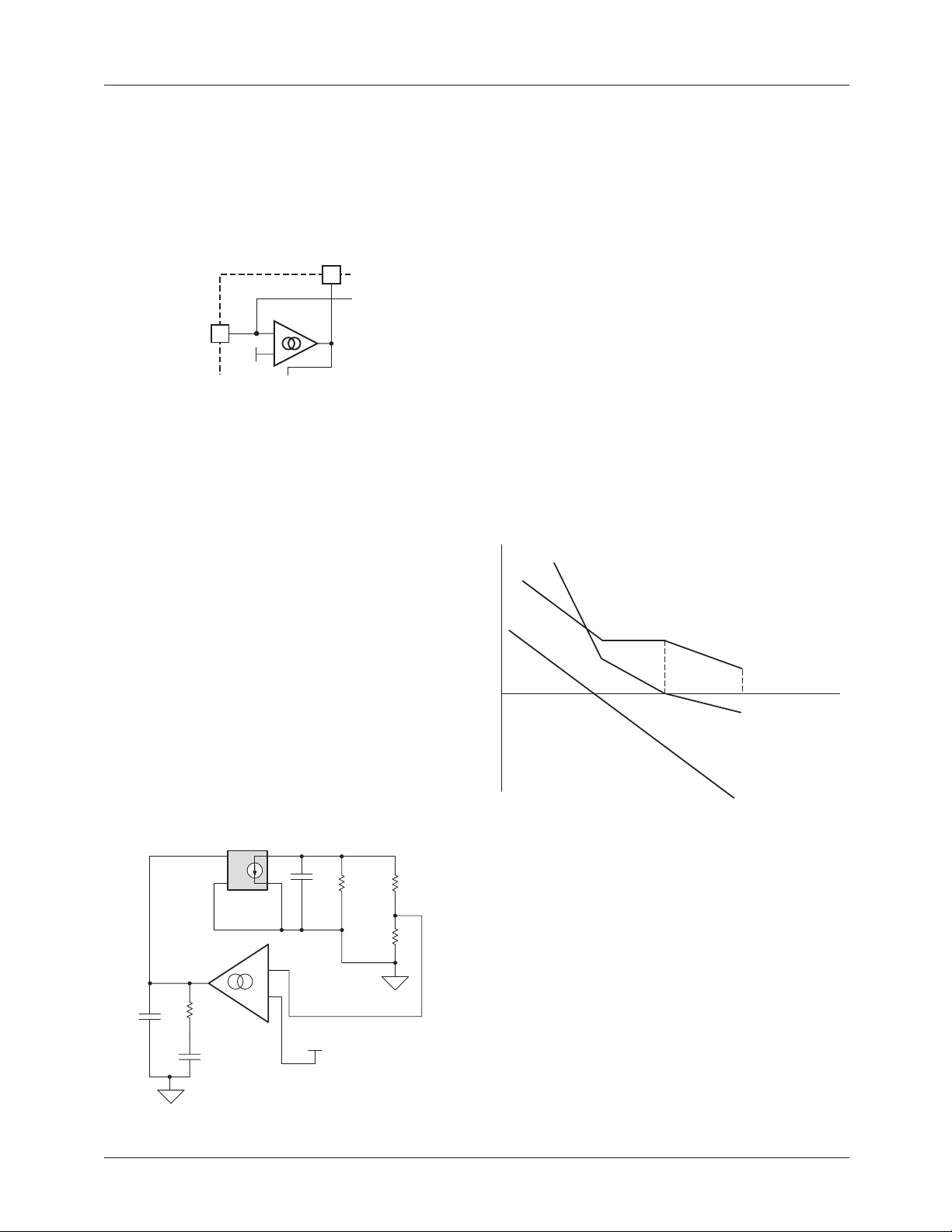
Figure 9 shows a simplified block diagram of the voltage
loop control. This approach is based on the notion that the
voltage control loop can be characterized by the voltage controlled current source feeding output capacitor. We assume
that the current loop generates full sine current waveforms
that feed capacitor C5 and a resistive load. The voltage error
amplifier controls the amplitude of this current and the entire
voltage loop closed around the current loop. In other words,
the voltage controlled current source combined together with
the input voltage source, rectifier, boost inductor, and diode
generates full sine waveforms with a magnitude proportional
to the output of the voltage error amplifier.
+
C5
2.5V
R_Load
R7
R8
C9
R11
C8
–
–
+
Gea Gea_fc
Gbst+Gvd
Gea_sh
Gclose_loop
R_SH
) across
1
Figure 10. Voltage Loop Bode Plots
fvl_z
110100
fc_vl
Let’s find the second harmonic voltage ripple (V
bulk capacitor C5.
P
= I
IN
--------=
V
O
IN_AV
× Z
(25)
O_SH
Z
O_SH
(27) dVEA = V
I
IN_AV
V
R_SH
Where f_ln is the line frequency, Z
---------------------------------------------------=
2 π× 2× f_ln× C5×
O_SH
the bulk capacitor at the second harmonic,V
second harmonic ripple voltage, dV
EA
range of the voltage error amplifier, V
1
– V
EA_OVH
EA_OVL
is the impedance of
is the
R_SH
is the output voltage
EA_OVH
and V
EA_OVL
are the voltage error amplifier’s maximum and minimum
output voltages respectively.
(26)
(28)
Figure 9. Simple Diagram of Voltage Loop
REV. 1.0.1 10/31/03 5
Page 6

AN6004 APPLICATION NOTE
According to the block diagram in Figure 9, the combined
gain of the voltage error amplifier and the resistor divider can
be shown as:
G
VD_EA
dVEATHD×
---------------------------------=
V
R_SH
Where THD is the total harmonics balance and dV
output range of the voltage amplifier.
G
VD
R7 R8+
G
is the voltage divider gain.
VD
(30)
R8
---------------------=
The following equation shows the gain of the voltage error
amplifier at the second harmonic.
G
EA_SH
G
EA_SH
Gvd_ea
-------------------= Z
Gvd
and Z
are error amplifier gain and impedance
EA_SH
EA_SH
G
-------------------=
g_va
EA_SH
at second harmonic frequency. g_va is voltage error amplifier transconductance. To ensure sufficient roll-off of voltage
gain at second harmonic frequency C9 is found from the
following expression.
2 π× 2× f_ln× Z
--------------------------------------------------------------=
C9
1
×
EA_SH
(32)
To find the values of R11 and C8, use the same approach
described above in a current loop. The following formula
defines gain of the boost section at crossover frequency
(G
G
BST_FC
A log equivalent of G
G
BST_FC_LOG
BT_FCS
).
I
IN_AV
-------------------------------------------------------------------=
= 20*log(G
1
--------------------------------------------
×
2 π× fc_vl× C5×
dV
EA
is:
BT_FCS
BST_FC
(33)
) (34)
The gain of the voltage divider in log form is shown in equation 35.
G
= 20*log(GVD) (35)
VD_LOG
The gain of the error amplifier in log form is determined by
the following expression:
G
EA_FC_LOG
= –(G
BST_FC_LOG
+ G
VD_LOG
) (36)
The gain of the error amplifier at cross-over frequency is:
EA
(29)
is the
(31)
0.9 G
R11
×
EA_FC
--------------------------------=
g_ea
(38)
C8
-----------------------------------------------=
2 π× fvl_z× R11×
1
(39)
This concludes the calculation and selection of power and
control components for PFC applications based on the
FAN4810 IC.
Step-by-step Instructions for
Selecting External Components for
a PFC Circuit
A PFC design tool is also available on Fairchild’s web site.
See www.fairchildsemi.com/xxxx for details.
Example Design of a FAN4810 Controller with
the Following Specifications
Po= 500W Output power
V
= 80 VAC Minimum voltage RMS
MIN
V
= 264 VAC Maximum voltage RMS
MAX
η = 0.93 Efficiency
Vo = 400 VDC Output (bus) voltage nominal value
V
fS = 100 kHz Switching frequency
T
THD = 5% Total Harmonics Distortion
dI
f_ln = 60 Hz Line frequency
FAN4810 specifications
tD = 500 ns Oscillator dead time
V
RMO = 3.6k Gain modulator output resistor
V
G
V
V
V
V
g_ea = 65 uS Voltage Error Amplifier
g_ca = 100 uS Current Error Amplifier
R
V
= 300 VDC Output (bus) voltage minimal value
O_MIN
= 20 ms Hold-up time
HDL
= 20% Ripple current
_RIPPLE
= 2.5V Oscillator Ramp Valley to Peak
RAMP
voltage
GM_OUT_MAX
= 2 Gain Modulator maximum gain
max
GM_IN_MAX
= 0.75V Gain modulator output voltage
= 1.1 V Gain Modulator input voltage that
produces maximum gain
= 2.5 V Voltage Error Amplifier reference
REF_EA
voltage
EA_OVH
= 6.7V Voltage Error Amplifier maximum
output voltage
= 0.1V Voltage Error Amplifier minimum
EA_OVL
output voltage
transconductance
transconductance
= 3.6 k Current Error Amplifier termination
GND
resistor
= 7.5V Reference voltage
REF
Gea_fc_log
-----------------------------
G
EA_FC
= (37)
10
20
6 REV. 1.0.1 10/31/03
Page 7

APPLICATION NOTE AN6004
Selecting the Power Components
Value of boost inductor L1 calculated based on formulas (1),
(2), (3), (4), (5).
P
= 537. 6 W I
IN
I_L
MAX_PK
= 10.45 A D = 0.717
_LINE_PK
= 9.5A dI = 1.9A
Calculated value of L1 is 426 µH. Value of inductor L1 = 420
µH is selected.
The value of bulk capacitor C5 is selected based on formula
(6). The calculated value of C5 = 2.857 µF. A standard value
of C5 = 330 µF/450V is selected for the bulk capacitor.
The value of the current sense resistor selected is based on
formula (15). The calculated value is 0.072 Ω. A standard
value R5 = 0.050 Ω is selected for the current sense resistor.
Parameters of current sense filter selected based on (16) R17
= 100 Ω, C19 = 0.047µF. Corner frequency of the filter,
calculated based on (16) is 33.8 kHz, that is inside the
specified range between 16.6 kHz and 100 kHz.
The boost diode D1 and switch Q1 are chosen for a voltage
rating of 500V or greater to withstand safely the 400V boost
potential. Current I_L
MAX_PK
= 10.45 A is also the peak
current for the boost diode D1 and switch Q1.
It is very difficult to recommend particular semiconductors
for specific applications, because these decisions are usually
made based on the unpredictable factors such as customer’s
inventory, airflow, and size of the heatsink. Refer to Table 1
for recommended MOSFETs, IGBTs and diodes.
Selecting Control Components
For setting the oscillator frequency value, R6 is calculated
based on formula (7) and the assumption C18 = 470 pF,
yields R6 = 41720 Ω. Let’s select a standard value
R6 = 41.2 k.
Selecting Parameters of Gain Modulator Input
Circuit
R1 is based on formula (8). To minimize the voltage rating of
each resistor, two 453K resistors in series are selected for
R1. The calculated value of R8 = 1.06 M.
Let’s use the same resistors that were selected above for
R2, R2 = 906 k and R3=100 k. R4 can be found using
formulas (9), (10), and (11). Vav = 72.1V, Ird1 = 70.5 µA,
R4 = 15.67 k. R4 = 15.8 k selected.
The value of capacitors C3, C2 are calculated based on
formulas (12), (13), and (14). Using these formulas
C3 = 1.035E-7 F and C2 = 5.11E-7 F. Standard values
C3 = 0.1 µF and C2 = 0.47 µF are selected.
Selection Parameters of Current Error
Amplifier Compensation Network
Let’s set fc_cl = 10.0 kHz, fcl_z = 2.0 kHz, fc_p = 100 kHz.
The value of R12 can be calculated based on (17) – (20).
G
PWM_BOOST
= 0.303, G
PWM_BOOST_LG
= -10.4, and
Gc_c = 3.3. R12 is determined to be 32.986 k. We will use a
standard value of R12 = 33.2 k. The values of C6 and C7 are
determined from (21) and (20). From these equations C6 is
found to be 2.392E-9 F and C7 is found to be 4.79E-11 F.
We will use 2.2 nF and 47 pF for C6 and C7, respectively
Selection Parameters of Voltage Error
Amplifier Compensation Network
Let’s assume R7 = 2.37 k, R8 is determined by (23, 24).
From equation 23, I
is found to be 1.055E-3 A, R7 is
RD2
determined to be 3.768E+5 Ω. To reduce the voltage across
each resistor, R7 is composed of three resistors of 127 k
each.
To determine the value of resistor C9, a number of intermediate variables should be calculated. Using expressions (25)
– (32), the following can be calculated:
G
VD_EA
= 0.045, G
EA_SH
= 7.33, Z
= 11.29E+4 Ω and
EA_SH
C9 = 1.17E-8 F is selected. A standard value of C9 = 0.01 µF
is selected.
To determine the values of R11 and C8 a number of intermediate variables should be calculated. Using expressions (33)
– (39), the following is calculated: G
G
BST_FC_LOG
31.13, G
= 12.9, G
= 36.7. R11 = 5.08E+5 and C8 = 1.117E-7 F.
EA_FC
VD_LOG
= -44.2, G
BST_FC
= 4.41,
EA_FC_LOG
=
Standard values of R11 = 510 k and C8 = 0.1µF are selected.
PFC Controller Application Tips
FAN4810 start-up takes place when C15 is charged to 13V
through R13 and R14. PFC switching action now boosts the
voltage on C5 to 400V via boost inductor L1. Through auxiliary winding of boost inductor L1, the circuit receives a
regulated 15V from a full wave rectifier that consists of D3,
D4, C12, and C16. For proper circuit operation, high frequency bypass capacitors are required on Vcc and V
Low ESR ceramic or film capacitors are highly recommended. Orderly PFC operation at start-up is guaranteed
when D2 quick charges C5 to the peak AC line voltage
before the boost switch Q1 turned on. This sequence ensures
the boost inductor current is zero before the PFC action
begins. The regulated voltage on C5 must always be greater
than the peak value of the maxi-mum line voltage delivered
to the supply.
The soft start circuit is comprised of components Q4, R16 and
C20. The error amplifier’s output voltage, V
, is forced to
EAO
follow the charging voltage of C20 by Q4. As C20 charges
toward V
tional to V
, Q4 is biased off. The PFC duty cycle is propor-
REF
, where zero V
EAO
gives zero duty cycle.
EAO
REF
.
REV. 1.0.1 10/31/03 7
Page 8
AN6004 APPLICATION NOTE
Circuit Performance
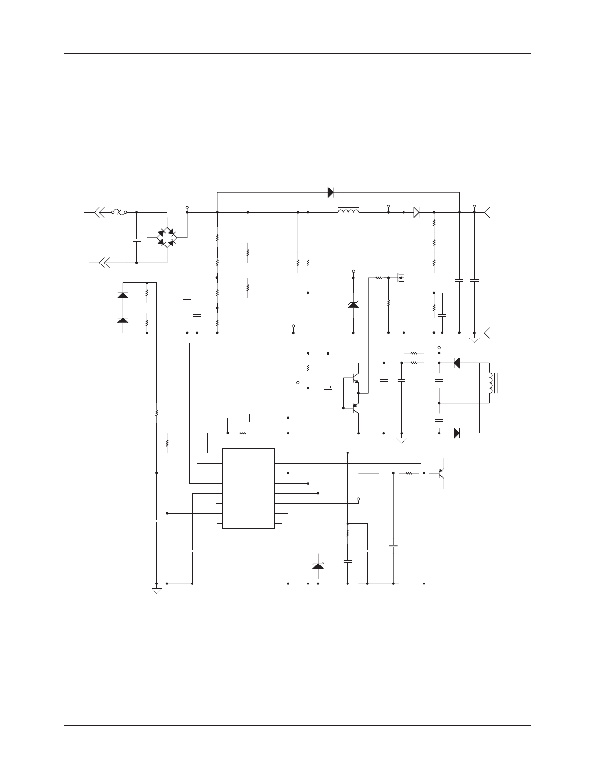
Figure 11 is a complete schematic of this application circuit.
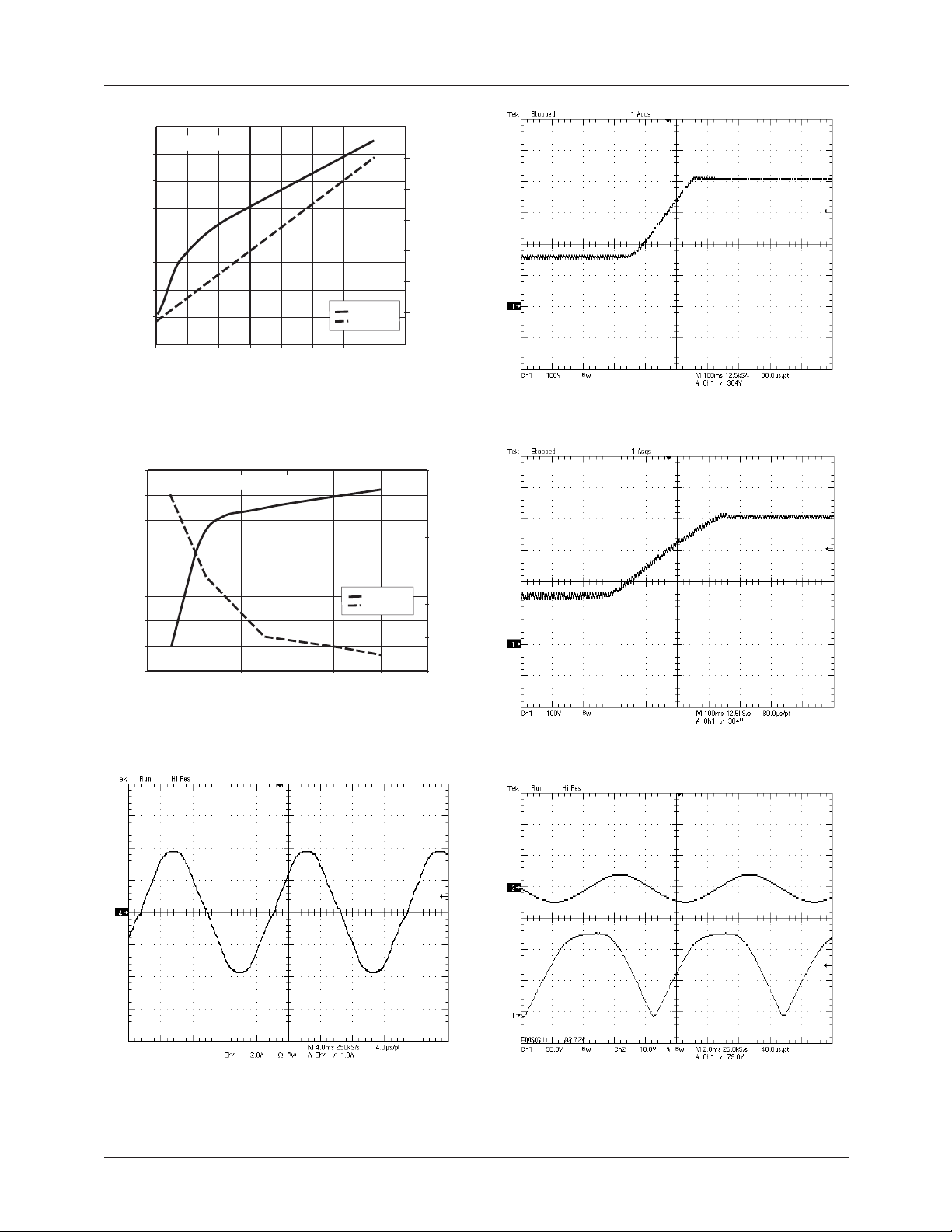
Figures 12 and 13 show the efficiency and THD performance. Figure 14 shows input current waveforms. Figures
15-17 show start-up waveforms.
D2 1N5406
R9
10k
C10
1.0µF
R18 10
C11
1.0µF
D1
ISL9R1560P2
Q1
FQA24N50
R10 47
C21
1.0µF
R16
200k
C20
1.0µF
R7A
127k
R7B
127k
R7C
127k
C5
330µF
C17
1.0nF
R8 2.37k
TP6
C12
1.0µF
C16
1.0µF
D3 RGF1A
D4
RGF1A
Q4
2N3906
TP2
C4
.047µF
6
5
R13
39k
2W
R15
0
C15
1500µF
L1 420µH
12, 11
1N4747A
D8
MBR052L
D5
2N3904
TP5
R11
510k
TP8
C8
.1µF
TP4
.47µF
C1
BR1
GBPC2506
R5A
.025
3W
R5B
.025
3W
R17
100
C19
.047µF
R6
41.2k
C18
470pF
R2A
453k
R2B
453k
R3
C3
100k
.1µF
C2
R4
.47µF
15.8k
1
2
3
4
5
6
7
89
C14
1.0µF
R1A
453k
R1B
453k
47pF
C7
R12 33.2k
C6 2.2nF
IEAO
IAC
ISENSE
VRMS
CLKSD
NC
RAMP1
NC GND
VEAO
VREF
VCC
PFC OUT
CLK OUT
GND
FAN4810
16
15
FB
14
13
12
11
10
R14
39k
2W
TP3
TP7
C13
1.0µF
F1
J1
AC INPUT
J2
D6
1N5401
D7
1N5401
7, 8
Q2
Q3
2N3906
R19 22
C9
.01µF
TP1
400VDC
J3
400VDCRTN
J4
L1
Figure 11. Schematic of 500W Power-Factor-Corrected Boost Converter
8 REV. 1.0.1 10/31/03
Page 9
APPLICATION NOTE AN6004
97
500 Watt Load
96
95
94
93
Efficiency (%)
92
91
90
89
90 110 130 150 170 190 210 230 250
Vline (RMS)
Efficiency
THD
Figure 12. Efficiency and THD Performance vs.
Input Line Voltage
98
96
94
92
90
88
Efficiency (%)
86
84
82
0 100 200 300 400 500 600
230 Vrms Line Voltage
Power Output (W)
Efficiency
THD
7.5
7
6.5
6
5.5
5
4.5
4
THD (%)
18
16
14
12
10
8
6
Figure 15. Turn-ON, Vo=405.3V, Io=0.5A
THD (%)
Figure 13. Efficiency and THD Performance vs.
Output Power
Figure 14. Input Current Waveform
Figure 16. Turn-ON, Vo=405.3V, Po=500W
Figure 17. Input Voltage and Output
Voltage Ripple Waveform
REV. 1.0.1 10/31/03 9
Page 10
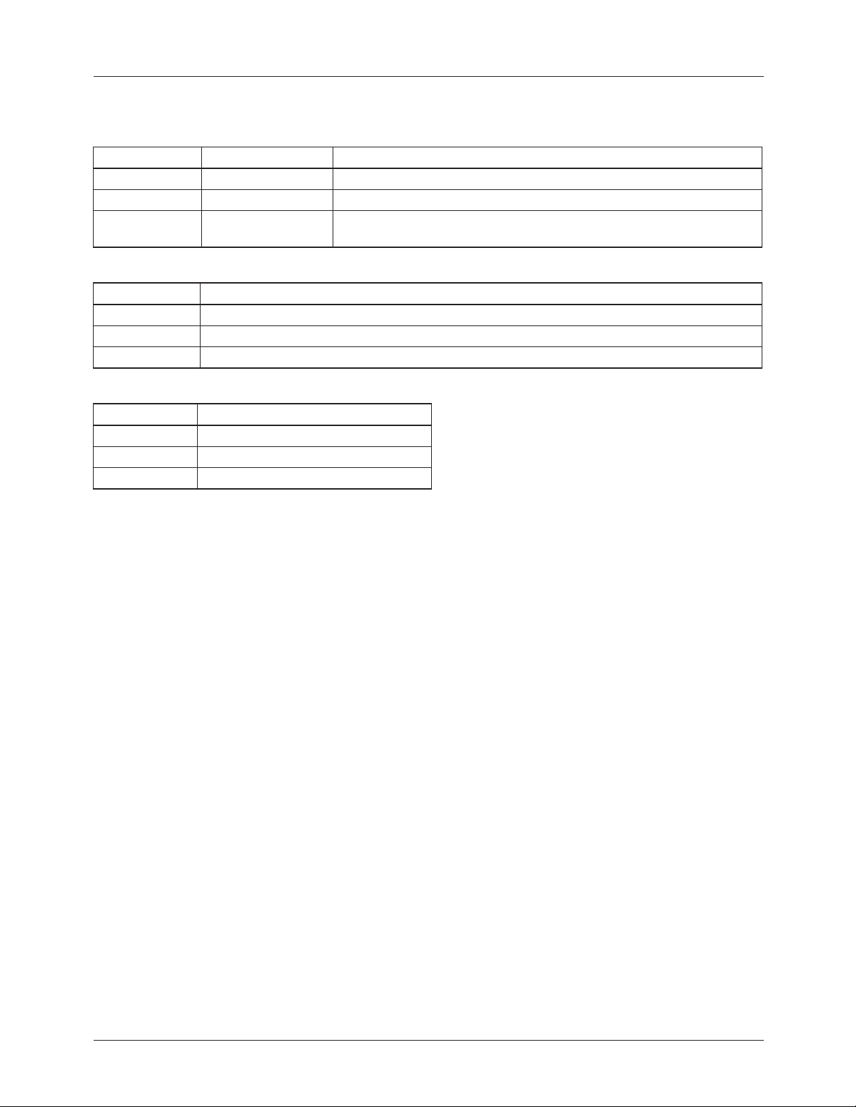
AN6004 APPLICATION NOTE
Table 1: Recommended Components
MOSFETs
Power Level Voltage rating P/Ns
75_100W 500,600V FQP6N50,FQP9N50, FQA13N50, FQA16N50,FDH15N50
100_400W 500,600V FQA16N50, FQA24N50, FQA19N60, FQA28N50
>400W 500,600V FDH44N50 ,FQL40N50, FQA28N50 , FDH27N50,
FQA19N60,FDH15N50 ,
IGBTs
Power Level P/Ns for frequency < 75 kHz
75_100W FGH20N6S2D,HGTG7N60A4D
100_400W FGH30N6S2D,HGTG12N60A4D
>400W FGH40N6S2D, HGTG20N60A4D, FGH50N6S2D, HGTG30N60A4D, FGK60N6S2D
Boost Diodes
Power Level P/Ns
75_100W ISL9R460P32 ISL9R860P2,
100_400W ISL9R860P2,ISL9R1560P2,
>400W ISL9R1560P2,ISL9R3060P2
DISCLAIMER
FAIRCHILD SEMICONDUCTOR RESERVES THE RIGHT TO MAKE CHANGES WITHOUT FURTHER NOTICE TO ANY
PRODUCTS HEREIN TO IMPROVE RELIABILITY, FUNCTION OR DESIGN. FAIRCHILD DOES NOT ASSUME ANY
LIABILITY ARISING OUT OF THE APPLICATION OR USE OF ANY PRODUCT OR CIRCUIT DESCRIBED HEREIN; NEITHER
DOES IT CONVEY ANY LICENSE UNDER ITS PATENT RIGHTS, NOR THE RIGHTS OF OTHERS.
LIFE SUPPORT POLICY
FAIRCHILD’S PRODUCTS ARE NOT AUTHORIZED FOR USE AS CRITICAL COMPONENTS IN LIFE SUPPORT DEVICES
OR SYSTEMS WITHOUT THE EXPRESS WRITTEN APPROVAL OF THE PRESIDENT OF FAIRCHILD SEMICONDUCTOR
CORPORATION. As used herein:
1. Life support devices or systems are devices or systems
which, (a) are intended for surgical implant into the body,
or (b) support or sustain life, or (c) whose failure to perform
when properly used in accordance with instructions for use
provided in the labeling, can be reasonably expected to
result in significant injury to the user.
2. A critical component is any component of a life support
device or system whose failure to perform can be
reasonably expected to cause the failure of the life support
device or system, or to affect its safety or effectiveness.
www.fairchildsemi.com
10/31/03 0.0m 002
2003 Fairchild Semiconductor Corporation
Stock#AN00006004
 Loading...