

Datasheet 5962R917230MFA, 5962R9172301VEA, 5962R9172301V2A, 5962R9172301MEA, 5962R9172301M2A Datasheet (NSC)
...Page 1
54AC163•54ACT163
Synchronous Presettable Binary Counter
General Description
The ’AC/’ACT163 are high-speed synchronous modulo-16
binary counters.They are synchronously presettable for application in programmable dividers and have two types of
Count Enable inputs plus a TerminalCount output for versatility in forming synchronous multistage counters. The ’AC/
’ACT163 has a Synchronous Reset input that overrides
counting and parallelloading and allows theoutputs to besimultaneously reset on the rising edge of the clock.
Features
n ICCreduced by 50
%
n Synchronous counting and loading
n High-speed synchronous expansion
n Typical count rate of 125 MHz
n Outputs source/sink 24 mA
n ’ACT163 has TTL-compatible inputs
n Standard Microcircuit Drawing (SMD)
— ’AC163: 5962-89582
— ’ACT163: 5962-91723
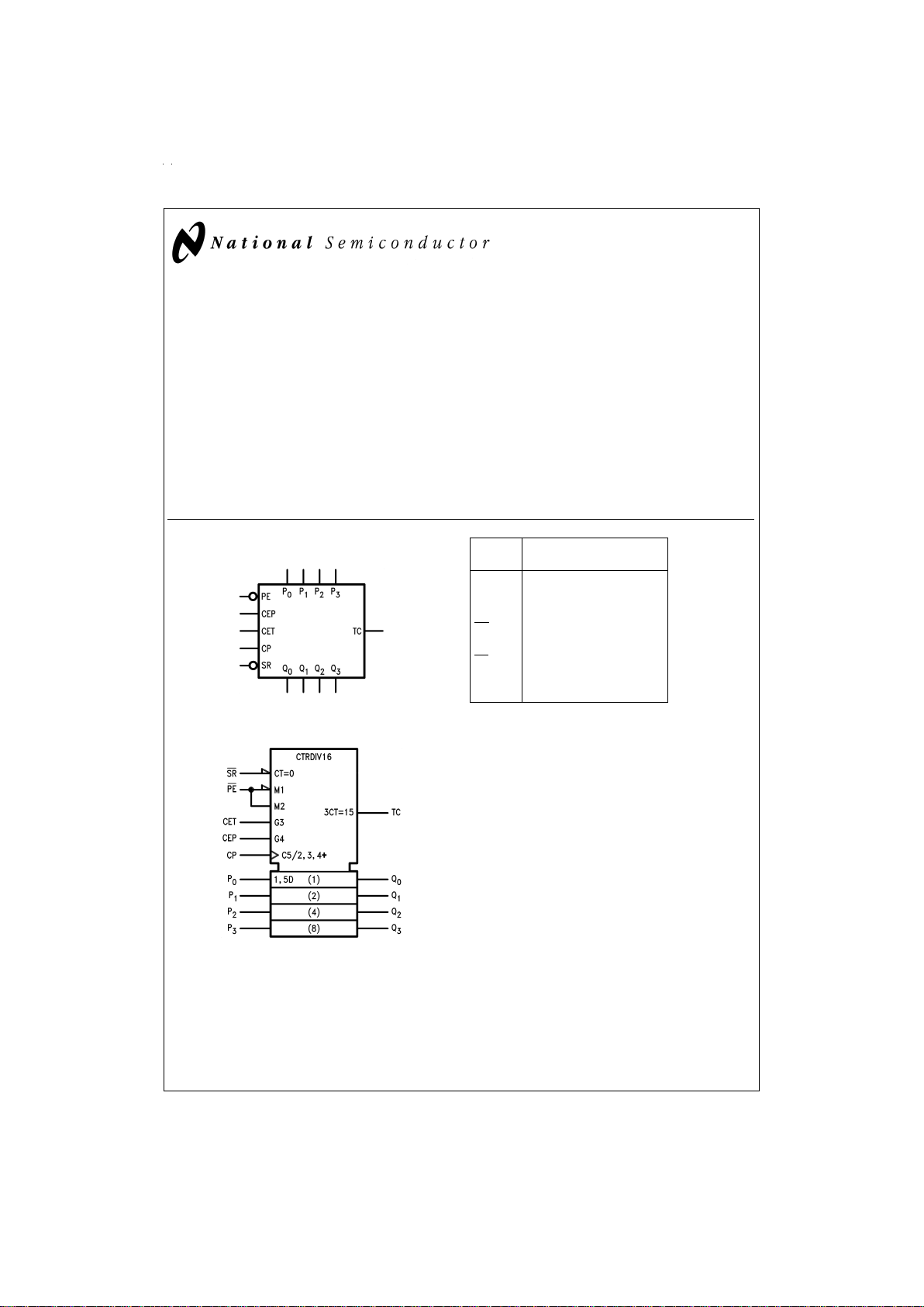
Logic Symbols
Pin
Names
Description
CEP Count Enable Parallel Input
CET Count Enable Trickle Input
CP Clock Pulse Input
SR
Synchronous Reset Input
P
0–P3
Parallel Data Inputs
PE
Parallel Enable Input
Q
0–Q3
Flip-Flop Outputs
TC Terminal Count Output
FACT™is a trademark of Fairchild Semiconductor Corporation.
DS100275-1
IEEE/IEC
DS100275-2
November 1998
54AC163
•
54ACT163 Synchronous Presettable Binary Counter
© 1998 National Semiconductor Corporation DS100275 www.national.com
Page 2
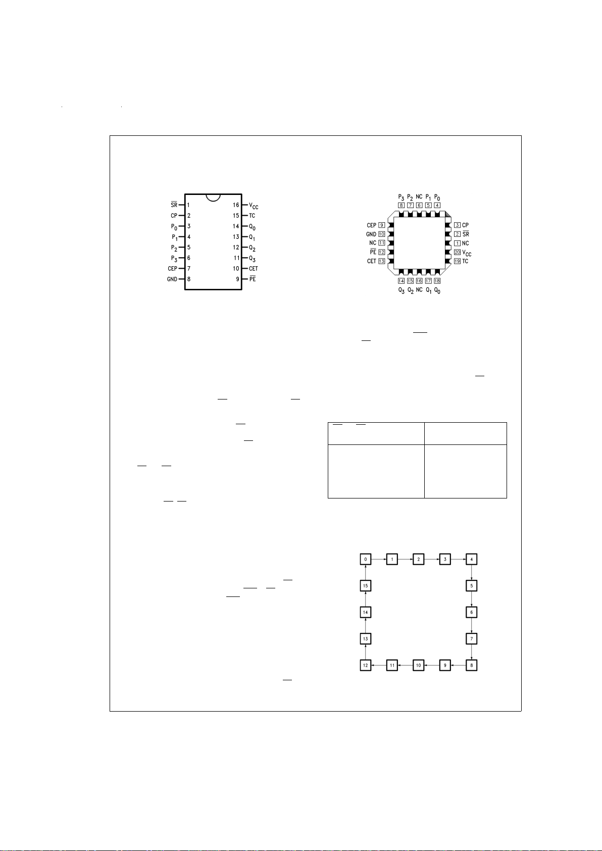
Connection Diagrams
Functional Description
The ’AC/’ACT163 counts in modulo-16 binary sequence.
From state 15 (HHHH) it increments to state 0 (LLLL). The
clock inputs of all flip-flops are driven in parallel through a
clock buffer.Thus all changesof the Q outputsoccur as a result of, and synchronouswith, the LOW-to-HIGH transitionof
the CP input signal. The circuits have four fundamental
modes of operation, inorder of precedence: synchronousreset, parallel load, count-up and hold. Four control
inputs—Synchronous Reset (SR), Parallel Enable (PE),
Count Enable Parallel (CEP) and Count Enable Trickle
(CET)—determine the mode of operation, as shown in the
Mode SelectTable. A LOW signal on SR overrides counting
and parallel loading and allowsall outputs togo LOW on the
next rising edgeof CP.ALOW signal on PE overrides counting and allowsinformation on theParallel Data (Pn) inputs to
be loaded into the flip-flops on the next rising edge of CP.
With PE and SR HIGH,CEP and CETpermit counting when
both are HIGH. Conversely, a LOW signal on either CEP or
CET inhibits counting.
The ’AC/’ACT163 uses D-type edge-triggered flip-flops and
changing the SR, PE, CEP and CET inputs when the CP is
in either state does not cause errors, provided that the recommended setup and hold times, with respect to the rising
edge of CP, are observed.
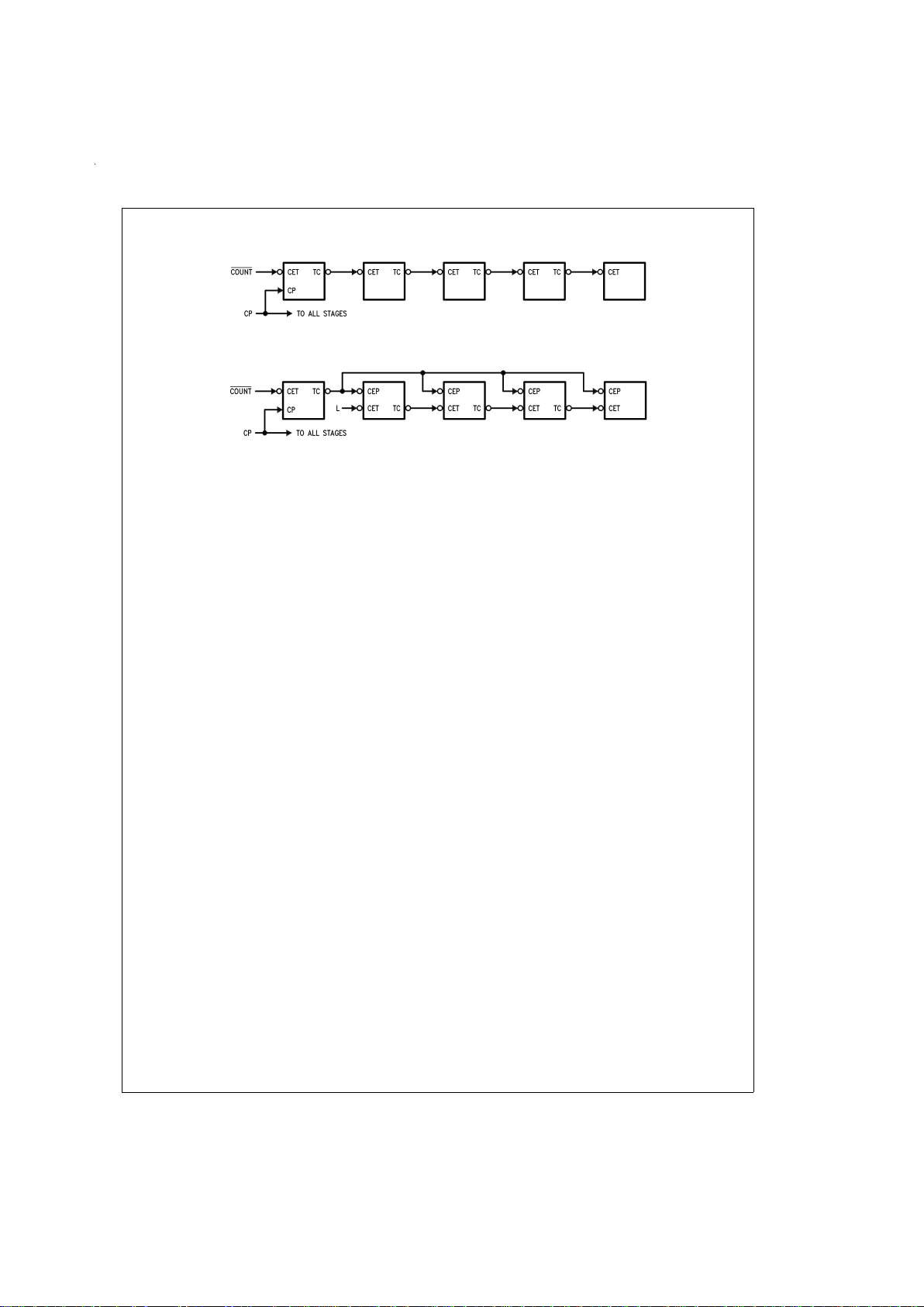
The Terminal Count (TC)output is HIGH when CET is HIGH
and counter is in state 15. To implement synchronous multistage counters, the TC outputs can be used with the CEP
and CET inputs in two different ways.
Figure 1
shows the connections for simple ripple carry, in
which the clockperiod must belonger than the CP to TCdelay of the firststage,plus the cumulative CETtoTC delays of
the intermediate stages, plus the CET to CP setup time of
the last stage.Thistotal delay plussetup time sets the upper
limit on clock frequency. For fasterclock rates, the carry lookahead connections shown in
Figure 2
are recommended. In
this scheme theripple delay throughthe intermediate stages
commences with the same clock that causes the first stage
to tick over from max to min in the Up mode, or min to max
in the Down mode, to start its final cycle. Since this final
cycle takes 16 clocks to complete, there is plenty of time for
the ripple to progress through the intermediate stages. The
critical timing that limits the clock period is the CP to TC de-
lay of the first stage plus the CEP to CP setup time of the last
stage. The TC output is subject to decoding spikes due to internal race conditions and is therefore not recommended for
use as a clock or asynchronous reset for flip-flops, registers
or counters.
Logic Equations: Count Enable=CEP
•
CET•PE
TC=Q
0
•
Q
1
•
Q
2
•
Q
3
•
CET
Mode Select Table
SR PE CET CEP Action on the Rising
Clock Edge (
N
)
L X X X Reset (Clear)
H L X X Load (P
n
→
Q
n
)
H H H H Count (Increment)
H H L X No Change (Hold)
H H X L No Change (Hold)
H=HIGH Voltage Level
L=LOW Voltage Level
X=Immaterial
State Diagram
Pin Assignment
for DIP and Flatpak
DS100275-3
Pin Assignment
for LCC
DS100275-4
DS100275-5
www.national.com 2
Page 3
State Diagram (Continued)
DS100275-8
FIGURE 1.
DS100275-9
FIGURE 2.
www.national.com3
Page 4
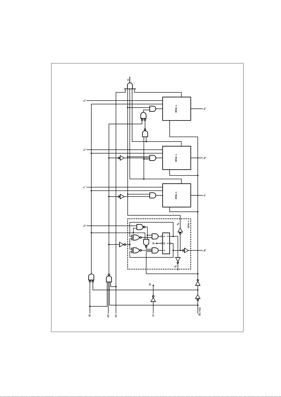
Block Diagram
DS100275-6
Please note that this diagram is provided only for the understanding of logic operations and should not be used to estimate propagation delays.
www.national.com 4
Page 5

Absolute Maximum Ratings (Note 1)
If Military/Aerospace specified devices are required,
please contact the National Semiconductor Sales Office/
Distributors for availability and specifications.
Supply Voltage (V
CC
) −0.5V to +7.0V
DC Input Diode Current (I
IK
)
V
I
=
−0.5V −20 mA
V
I
=
V
CC
+ 0.5V +20 mA
DC Input Voltage (V
I
) −0.5V to VCC+ 0.5V
DC Output Diode Current (I
OK
)
V
O
=
−0.5V −20 mA
V
O
=
V
CC
+ 0.5V +20 mA
DC Output Voltage (V
O
) −0.5V to VCC+ 0.5V
DC Output Source
or Sink Current (I
O
)
±
50 mA
DC V
CC
or Ground Current
per Output Pin (I
CC
or I
GND
)
±
50 mA
Storage Temperature (T
STG
) −65˚C to +150˚C
Junction Temperature (T
J
)
CDIP 175˚C
Recommended Operating
Conditions
Supply Voltage (VCC)
’AC 2.0V to 6.0V
’ACT 4.5V to 5.5V
Input Voltage (V
I
) 0VtoV
CC
Output Voltage (VO) 0VtoV
CC
Operating Temperature (TA)
54AC/ACT −55˚C to +125˚C
Minimum Input Edge Rate (∆V/∆t)
’AC Devices
V
IN
from 30%to 70%of V
CC
V
CC
@
3.3V, 4.5V, 5.5V 125 mV/ns
Minimum Input Edge Rate (∆V/∆t)
’ACT Devices
V
IN
from 0.8V to 2.0V
V
CC
@
4.5V, 5.5V 125 mV/ns
Note 1: Absolute maximum ratings are those values beyond which damage
to the device may occur. The databook specifications should be met, without
exception, to ensure that the system design is reliable over its power supply,
temperature, and output/input loading variables. National does not recommend operation of FACT
™
circuits outside databook specifications.
DC Characteristics for ’AC Family Devices
54AC
Symbol Parameter V
CC
T
A
=
Units Conditions
(V) −55˚C to +125˚C
Guaranteed
Limits
V
IH
Minimum High Level 3.0 2.1 V
OUT
=
0.1V
Input Voltage 4.5 3.15 V or V
CC
− 0.1V
5.5 3.85
V
IL
Maximum Low Level 3.0 0.9 V
OUT
=
0.1V
Input Voltage 4.5 1.35 V or V
CC
− 0.1V
5.5 1.65
V
OH
Minimum High Level 3.0 2.9 I
OUT
=
−50 µA
Output Voltage 4.5 4.4 V
5.5 5.4
(Note 2)
V
IN
=
V
IL
or V
IH
3.0 2.4 IOH= −12 mA
4.5 3.7 V I
OH
= −24 mA
5.5 4.7 I
OH
= −24 mA
V
OL
Maximum Low Level 3.0 0.1 I
OUT
=
50 µA
Output Voltage 4.5 0.1 V
5.5 0.1
(Note 2)
V
IN
=
V
IL
or V
IH
3.0 0.50 IOL=12mA
4.5 0.50 V I
OL
=24mA
5.5 0.50 I
OL
=24mA
I
IN
Maximum Input 5.5
±
1.0 µA V
I
=
V
CC
, GND
Leakage Current
I
OLD
Minimum Dynamic
Output Current (Note 3)
5.5 50 mA V
OLD
=
1.65V Max
I
OHD
5.5 −50 mA V
OHD
=
3.85V Min
www.national.com5
Page 6

DC Characteristics for ’AC Family Devices (Continued)
54AC
Symbol Parameter V
CC
T
A
=
Units Conditions
(V) −55˚C to +125˚C
Guaranteed
Limits
I
CC
Maximum Quiescent 5.5 160 µA V
IN
=
V
CC
Supply Current or GND
Note 2: All outputs loaded; thresholds on input associated with output under test.
Note 3: Maximum test duration 2.0 ms, one output loaded at a time.
Note 4: I
IN
and I
CC
@
3.0V are guaranteed to be less than or equal to the respective limit@5.5V VCC.
I
CC
for 54AC@25˚C is identical to 74AC@25˚C.
DC Characteristics for ’ACT Family Devices
54ACT
Symbol Parameter V
CC
T
A
=
Units Conditions
(V) −55˚C to +125˚C
Guaranteed
Limits
V
IH
Minimum High Level 4.5 3.0 V V
OUT
=
0.1V
Input Voltage (Note 7) 5.5 3.0 or V
CC
− 0.1V
V
IL
Maximum Low Level 4.5 0.8 V V
OUT
=
0.1V
Input Voltage 5.5 0.8 or V
CC
− 0.1V
V
OH
Minimum High Level 4.5 4.4 V I
OUT
=
−50 µA
Output Voltage 5.5 5.4
(Note 5)
V
IN
=
V
IL
or 3.0V
4.5 3.70 V I
OH
= −24 mA
5.5 4.70 I
OH
= −24 mA
V
OL
Maximum Low Level 4.5 0.1 V I
OUT
=
50 µA
Output Voltage 5.5 0.1
(Note 5)
V
IN
=
V
IL
or V
IH
4.5 0.50 V IOL=24mA
5.5 0.50 I
OL
=24mA
I
IN
Maximum Input 5.5
±
1.0 µA V
I
=
V
CC
, GND
Leakage Current
I
CCT
Maximum 5.5 1.6 mA V
I
=
V
CC
− 2.1V
I
CC
/Input
I
OLD
Minimum Dynamic
Output Current (Note 6)
5.5 50 mA V
OLD
=
1.65V Max
I
OHD
5.5 −50 mA V
OHD
=
3.85V Min
I
CC
Maximum Quiescent 5.5 80.0 µA V
IN
=
V
CC
Supply Current or GND
Note 5: All outputs loaded; thresholds on input associated with output under test.
Note 6: Maximum test duration 2.0 ms, one output loaded at a time.
Note 7: For dynamic operation, a V
IH
level between 2.0 and 3.0V may be recognized by this device as a high logic level input. For static operation, a VIH≥ 2.0V will
be recognized by this device as a high logic level input. Users are cautioned to verify that this will not affect their system.
www.national.com 6
Page 7

AC Electrical Characteristics
54AC
V
CC
T
A
=
−55˚C
Symbol Parameter (V) to +125˚C Units
(Note 8) C
L
=
50 pF
Min Max
f
max
Maximum Clock 3.3 55 MHz
Frequency 5.0 90
t
PLH
Propagation Delay, CP to Q
n
3.3 1.0 13.5 ns
(PE Input HIGH or LOW)
5.0 1.5 9.5
t
PHL
Propagation Delay, CP to Q
n
3.3 1.0 12.5 ns
(PE Input HIGH or LOW)
5.0 1.5 9.5
t
PLH
Propagation Delay 3.3 1.0 16.5 ns
CP to TC 5.0 1.5 11.0
t
PHL
Propagation Delay 3.3 1.0 15.0 ns
CP to TC 5.0 1.5 11.0
t
PLH
Propagation Delay 3.3 1.0 11.0 ns
CET to TC 5.0 1.5 7.5
t
PHL
Propagation Delay 3.3 1.0 12.0 ns
CET to TC 5.0 1.5 9.0
Note 8: Voltage Range 3.3 is 3.3V±0.3V
Voltage Range 5.0 is 5.0V
±
0.5V
AC Operating Requirements
54AC
V
CC
T
A
=
−55˚C
Symbol Parameter (V) to +125˚C Units
(Note 9) C
L
=
50 pF
Guaranteed Minimum
t
s
Setup Time, HIGH or LOW 3.3 17.0 ns
P
n
to CP 5.0 11.0
t
h
Hold Time, HIGH or LOW 3.3 −0.5 ns
P
n
to CP 5.0 0
t
s
Setup Time, HIGH or LOW 3.3 17.0 ns
SR to CP
5.0 12.0
t
h
Hold Time, HIGH or LOW 3.3 −0.5 ns
SR to CP
5.0 0
t
s
Setup Time, HIGH or LOW 3.3 16.0 ns
PE to CP
5.0 9.5
t
h
Hold Time, HIGH or LOW 3.3 −0.5 ns
PE to CP
5.0 0
t
s
Setup Time, HIGH or LOW 3.3 8.0 ns
CEP or CET to CP 5.0 5.5
t
h
Hold Time, HIGH or LOW 3.3 0 ns
CEP or CET to CP 5.0 0.5
t
w
Clock Pulse Width (Load) 3.3 5.0 ns
HIGH or LOW 5.0 5.0
t
w
Clock Pulse Width (Count) 3.3 5.0 ns
HIGH or LOW 5.0 5.0
Note 9: Voltage Range 3.3 is 3.3V±0.3V
Voltage Range 5.0 is 5.0V
±
0.5V
www.national.com7
Page 8

AC Electrical Characteristics
54ACT
V
CC
T
A
=
−55˚C
Symbol Parameter (V) to +125˚C Units
(Note 10) C
L
=
50 pF
Min Max
f
max
Maximum Clock 5.0 90 MHz
Frequency
t
PLH
Propagation Delay, CP to Q
n
5.0 1.5 10.5 ns
(PE Input HIGH or LOW)
t
PHL
Propagation Delay, CP to Q
n
5.0 1.5 10.5 ns
(PE Input HIGH or LOW)
t
PLH
Propagation Delay 5.0 1.5 12.5 ns
CP to TC
t
PHL
Propagation Delay 5.0 1.5 13.0 ns
CP to TC
t
PLH
Propagation Delay 5.0 1.5 9.5 ns
CET to TC
t
PHL
Propagation Delay 5.0 1.5 9.5 ns
CET to TC
Note 10: Voltage Range 5.0 is 5.0V±0.5V
AC Operating Requirements
54ACT
V
CC
T
A
=
−55˚C
Symbol Parameter (V) to +125˚C Units
(Note 11) C
L
=
50 pF
Guaranteed
Minimum
t
s
Setup Time, HIGH or LOW 5.0 13.5 ns
P
n
to CP
t
h
Hold Time, HIGH or LOW 5.0 0.5 ns
P
n
to CP
t
s
Setup Time, HIGH or LOW 5.0 13.5 ns
SR to CP
t
h
Hold Time, HIGH or LOW 5.0 0.0 ns
SR to CP
t
s
Setup Time, HIGH or LOW 5.0 11.5 ns
PE to CP
t
h
Hold Time, HIGH or LOW 5.0 0.0 ns
PE to CP
t
s
Setup Time, HIGH or LOW 5.0 7.0 ns
CEP or CET to CP
t
h
Hold Time, HIGH or LOW 5.0 0.5 ns
CEP or CET to CP
t
w
Clock Pulse Width (Load) 5.0 5.0 ns
HIGH or LOW
t
w
Clock Pulse Width 5.0 5.0 ns
(Count) HIGH or LOW
Note 11: Voltage Range 5.0 is 5.0V±0.5V
www.national.com 8
Page 9

Capacitance
Symbol Parameter Typ Units Conditions
C
IN
Input Capacitance 4.5 pF V
CC
=
OPEN
C
PD
Power Dissipation 45.0 pF V
CC
=
5.0V
Capacitance
www.national.com9
Page 10

10
Page 11

Physical Dimensions inches (millimeters) unless otherwise noted
20 Terminal Ceramic Leadless Chip Carrier (L)
NS Package Number E20A
16-Lead Ceramic Dual-In-Line Package (D)
NS Package Number J16A
www.national.com11
Page 12

Physical Dimensions inches (millimeters) unless otherwise noted (Continued)
LIFE SUPPORT POLICY
NATIONAL’S PRODUCTS ARE NOT AUTHORIZED FOR USE AS CRITICAL COMPONENTS IN LIFE SUPPORT DEVICES OR SYSTEMS WITHOUT THE EXPRESS WRITTEN APPROVAL OF THE PRESIDENT OF NATIONAL SEMICONDUCTOR CORPORATION. As used herein:
1. Life support devices or systems are devices or systems which, (a) are intended for surgical implant into
the body, or (b) support or sustain life, and whose failure to perform when properly used in accordance
with instructions for use provided in the labeling, can
be reasonably expected to result in a significant injury
to the user.
2. A critical component in any component of a life support
device or system whose failure to perform can be reasonably expected to cause the failure of the life support
device or system, or to affect its safety or effectiveness.
National Semiconductor
Corporation
Americas
Tel: 1-800-272-9959
Fax: 1-800-737-7018
Email: support@nsc.com
www.national.com
National Semiconductor
Europe
Fax: +49 (0) 1 80-530 85 86
Email: europe.support@nsc.com
Deutsch Tel: +49 (0) 1 80-530 85 85
English Tel: +49 (0) 1 80-532 78 32
Français Tel: +49 (0) 1 80-532 93 58
Italiano Tel: +49 (0) 1 80-534 16 80
National Semiconductor
Asia Pacific Customer
Response Group
Tel: 65-2544466
Fax: 65-2504466
Email: sea.support@nsc.com
National Semiconductor
Japan Ltd.
Tel: 81-3-5620-6175
Fax: 81-3-5620-6179
16-Lead Ceramic Flatpak (F)
NS Package Number W16A
54AC163
•
54ACT163 Synchronous Presettable Binary Counter
National does not assume any responsibility for use of any circuitry described, no circuit patent licenses are implied and National reserves the right at any time without notice to change said circuitry and specifications.
 Loading...