

Datasheet 5962R3829437SNC, 5962R3829437SNA, 5962R3829437BXX, 5962R3829437BXC, 5962R3829437BNX Datasheet (UTMC)
...Page 1
FEATURES
q 55ns maximum address access time, single-event upset less
than 1.0E-10 errors//bit day (-55oC to 125+oC)
q Asynchronous operation for compatibility with industry-
standard 8K x 8 SRAM
q TTL-compatible input and output levels
q Three-state bidirectional data bus
q Low operating and standby current
q Full military operating temperature range, -55oC to 125+oC,
screened to specific test methods listed in Table I MIL-STD883 Method 5004 for Class S or Class B
q Radiation-hardened process and design; total dose irradiation
testing to MIL-STD-883 Method 1019
- Total-dose: 1.0E6 rads(Si)
- Dose rate upset: 1.0E9 rads (Si)/sec
- Dose rate survival: 1.0E12 rads (Si)/sec
- Single-event upset: <1.0E-10 errors/bit-day
q Industry standard (JEDEC) 64K SRAM pinout
q Packaging options:
- 28-pin 100-mil center DIP (.600 x 1.2)
- 28-pin 50-mil center flatpack (.700 x .75)
q 5-volt operation
q Post-radiation AC/DC performance characteristics
guaranteed by MIL-STD-883 Method 1019 testing at
1.0E6 rads(Si)
INTRODUCTION
The UT67164 SRAM is a high performance, asynchronous,
radiation-hardened, 8K x 8 random access memory
conforming to industry-standard fit, form, and function. The
UT67164 SRAM features fully static operation requiring no
external clocks or timing strobes. UTMC designed and
implemented the UT67164 using an advanced radiationhardened twin-well CMOS process. Advanced CMOS
processing along with a device enable/disable function
result in a high performance, power-saving SRAM. The
combination of radiation-hardness, fast access time, and low
power consumption make UT67164 ideal for high-speed
systems designed for operation in radiation environments.
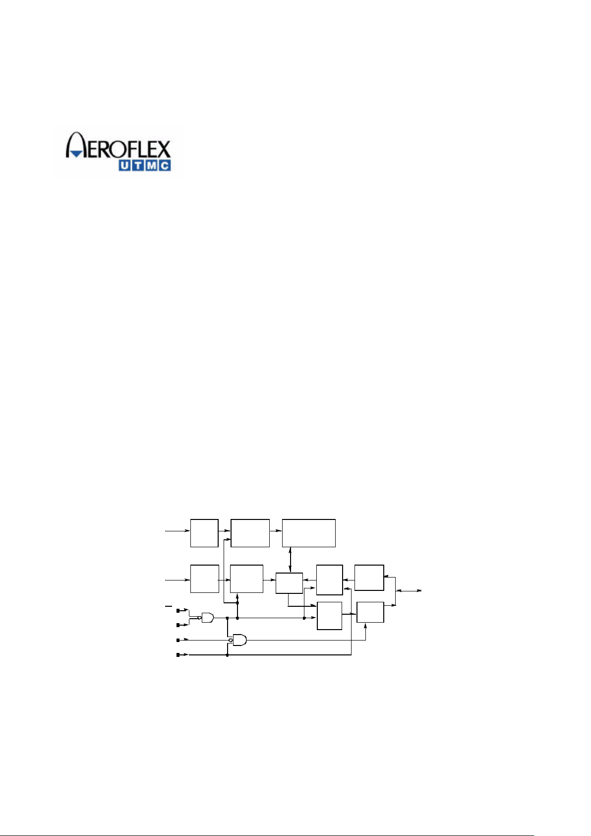
INPUT
DRIVERS
256 x 256
MEMORY ARRAY
COLUMN
I/O
Figure 1. SRAM Block Diagram
INPUT
DRIVERS
A(4:0)
INPUT
DRIVERS
A(12:5)
ROW
DECODERS
OUTPUT ENABLE
E2
W
G
E1
CHIP ENABLE
OUTPUT
DRIVERS
DATA
WRITE
CIRCUIT
DATA
READ
CIRCUIT
DQ(7:0)
COLUMN
DECODERS
WRITE ENABLE
Standard Products
UT67164 Radiation-Hardened 8K x 8 SRAM -- SEU Hard
Data Sheet
January 2002
Page 2
2
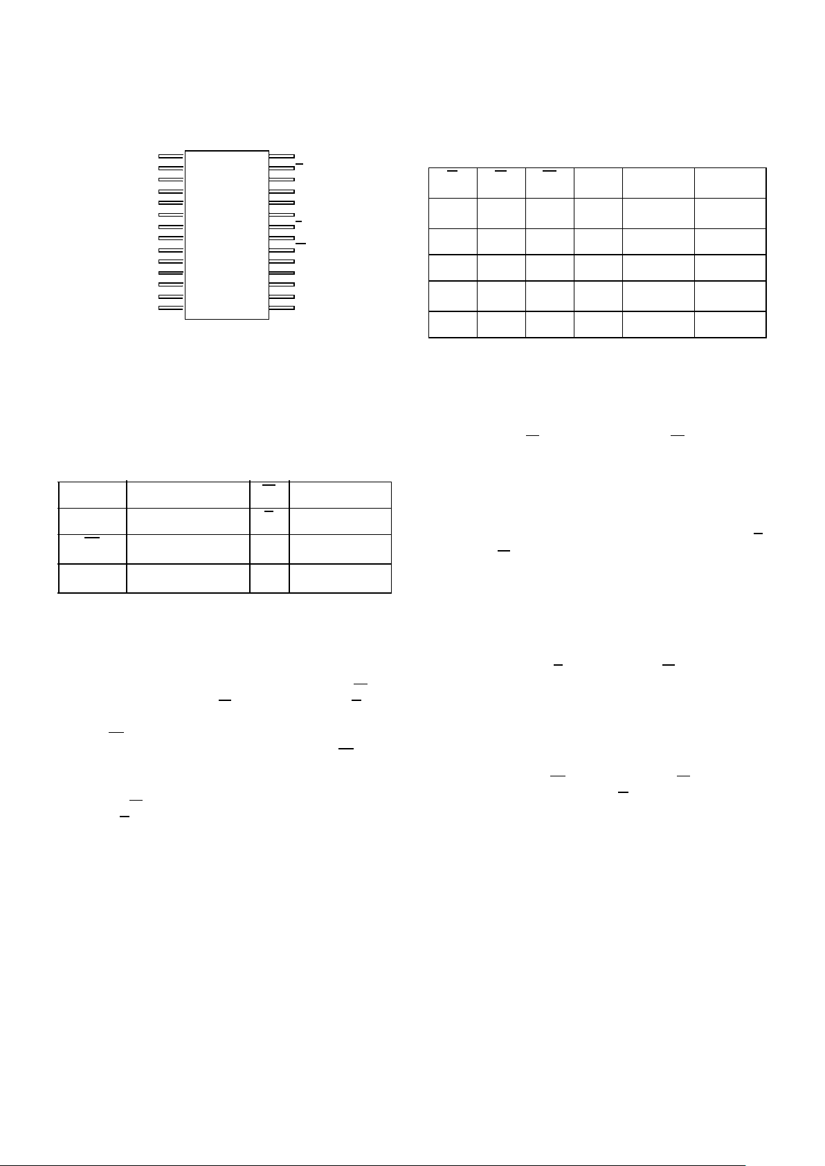
PIN NAMES
DEVICE OPERATION
The UT67164 has four control inputs called Enable 1 (E1),
Enable 2 (E2), Write Enable (W), and Output Enable (G); 13
address inputs, A(12:0); and eight bidirectional data lines,
DQ(7:0). E1 and E2 are device enable inputs that control device
selection, active, and standby modes. Asserting both E1 and E2
enables the device, causes I
DD
to rise to its active value, and
decodes the 13 address inputs to select one of 8,192 words in
the memory. W controls read and write operations. During a
read cycle, G must be asserted to enable the outputs.
Table 1. Device Operation Truth Table
Notes:
1. “X” is defined as a “don’t care” condition.
2. Device active; outputs disabled.
READ CYCLE
A combination of W greater than V
IH
(min), E1 less than V
IL
(max), and E2 greater than V
IH
(min) defines a read cycle. Read
access time is measured from the latter of device enable, Output
Enable, or valid address to valid data output.
Read Cycle 1, the Address Access read in figure 3a, is initiated
by a change in address inputs while the chip is enabled with G
asserted and W deasserted. Valid data appears on data outputs
DQ(7:0) after the specified t
AVQV
is satisfied. Outputs remain
active throughout the entire cycle. As long as device enable and
output enable are active, the address inputs may change at a rate
equal to the minimum read cycle time (t
AVAV
).
Figure 3b shows Read Cycle 2, the Chip Enable-controlled
Access. For this cycle, G remains asserted, W remains
deasserted, and the addresses remain stable for the entire cycle.
After the specified t
ETQV
is satisfied, the eight-bit word
addressed by A(12:0) is accessed and appears at the data outputs
DQ(7:0).
Figure 3c shows Read Cycle 3, the Output Enable-controlled
Access. For this cycle, E1 and E2 are asserted, W is deasserted,
and the addresses are stable before G is enabled. Read access
time is t
GLQV
unless t
AVQV
or t
ETQV
have not been satisfied.
A(12:0) Address W Write
DQ(7:0) Data Input/Output G Output Enable
E1 Enable 1 V
DD
Power
E2
1
Enable 2 V
SS
Ground
1 28
2 27
3 26
4 25
5 24
6 23
7 22
8 21
9 20
10 19
11 18
12 17
13 16
14 15
Figure 2. SRAM Pinout
NC
A12
A7
A6
A5
A4
A3
A2
A1
A0
DQ0
DQ1
DQ2
Vss
VDD
W
E2
A8
A9
A11
G
A10
E1
DQ7
DQ6
DQ5
DQ4
DQ3
G W E1
E2
I/O Mode Mode
X1
X X 0 3-state Standby
X X 1 X 3-state Standby
X 0 0 1 Data in Write
1 1 0 1 3-state
Read
2
0 1 0 1 Data out Read
Page 3
3
WRITE CYCLE
A combination of W less than VIL(max), E1 less than VIL(max),
and E2 greater than VIH(min) defines a write cycle. The state of
G is a “don’t care” for a write cycle. The outputs are placed in
the high-impedance state when either G is greater than
VIH(min), or when W is less than VIL(max).
Write Cycle 1, the Write Enable-controlled Access shown in
figure 4a, is defined by a write terminated by W going high, with
E1 and E2 still active. The write pulse width is defined by t
WLWH
when the write is initiated by W, and by t
ETWH
when the write
is initiated by the latter of E1 or E2. Unless the outputs have
been previously placed in the high-impedance state by G, the
user must wait t
WLQZ
before applying data to the eight
bidirectional pins DQ(7:0) to avoid bus contention.
Write Cycle 2, the Chip Enable-controlled Access shown in
figure 4b, is defined by a write terminated by the latter of E1 or
E2 going inactive. The write pulse width is defined by t
WLEF
when the write is initiated by W, and by t
ETEF
when the write
is initiated by the latter of E1 or E2 going active. For the W
initiated write, unless the outputs have been previously placed
in the high-impedance state by G, the user must wait t
WLQZ
before applying data to the eight bidirectional pins DQ(7:0) to
avoid bus contention.
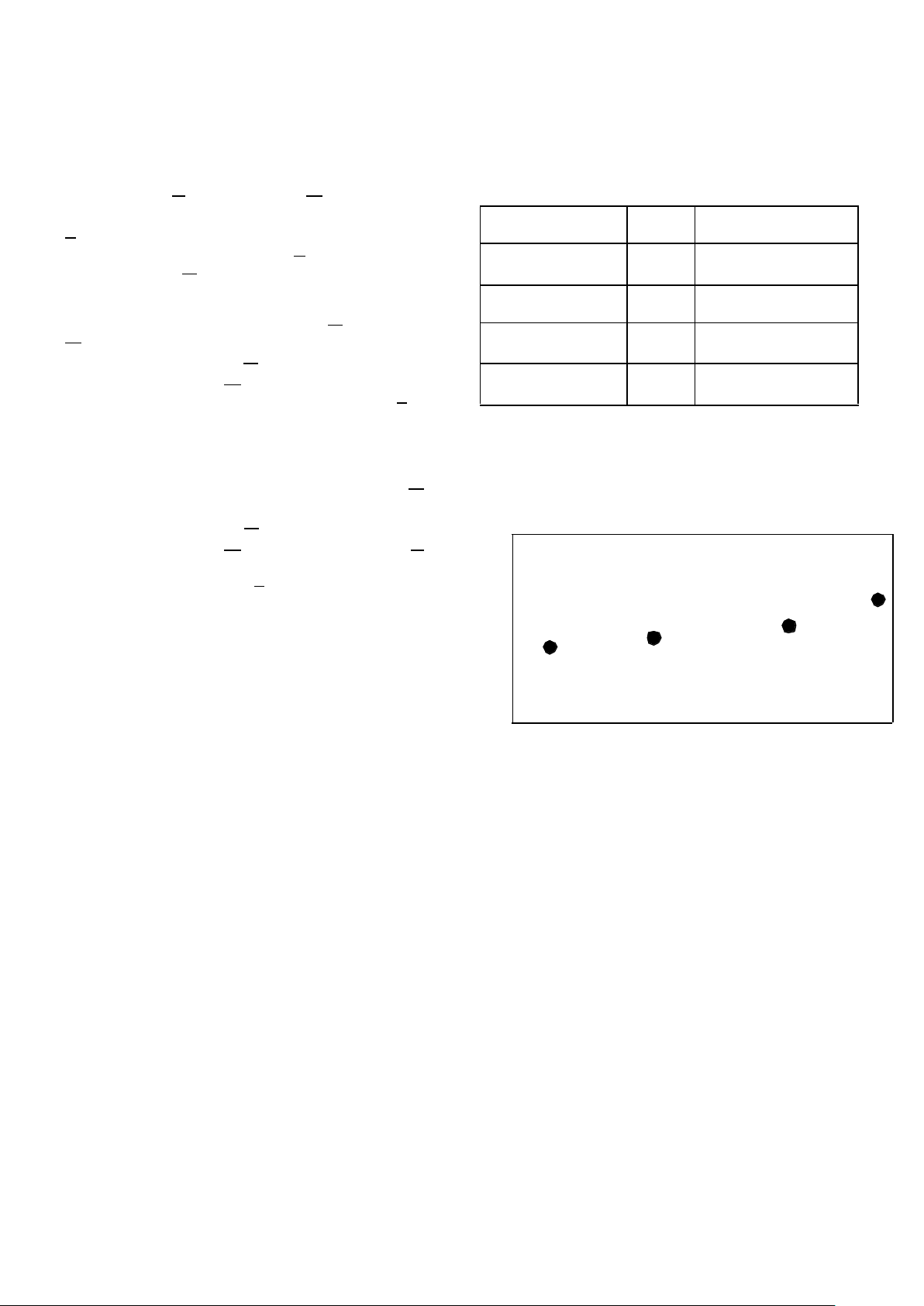
RADIATION HARDNESS
The UT67164 SRAM incorporates special design and layout
features which allow operation in high-level radiation
environments.
Table 2. Radiation Hardness
Design Specifications
1
Notes:
1. The SRAM will not latchup during radiation exposure under recommended
operating conditions.
2. 90% Adam’s worst case spectrum (-55oC to 125+oC).
Total Dose 1.0E6 rads(Si)
Dose Rate Upset
1.0E9 rads(Si)/s 20ns pulse
Dose Rate Survival 1.0E12 rads(Si)/s 20ns pulse
Single-Event Upset 1.0E-10
errors/bit day
2
Neutron Fluencs 3.0E14
n/cm
2
Table 3. SEU versus Temperature
SEU
errors/bit-day
10
-4
10
-6
10
-8
10
-10
10
-10
10
-13
10
-11
10
-1210-13
10
-14
10
-16
-55 -35 -15 5 25 45 65 85 105 125
Temperature (oC)
Page 4
4
ABSOLUTE MAXIMUM RATINGS
1
(Referenced to VSS)
Notes:
1. Stresses outside the listed absolute maximum ratings may cause permanent damage to the device. This is a stress rating only, and functional operation of the device
at these or any other conditions beyond limits indicated in the operational sections of this specification is not recommended. Exposure to absolute maximum rating
conditions for extended periods may affect device reliability.
2. Test per MIL-STD-883, Method 1012.
RECOMMENDED OPERATING CONDITIONS
SYMBOL PARAMETER LIMITS
V
DD
DC supply voltage -0.5 to 7.0V
V
I/O
Voltage on any pin -0.5 to V
DD
+ 0.5
T
STG
Storage temperature -65 to +150°C
P
D
Maximum power dissipation 1.0W
T
J Maximum junction temperature
+150°C
Θ
JC
Thermal resistance, junction-to-case
2
10°C/W
I
LU
Latchup immunity +/-150mA
I
I
DC input current
+/-10 mA
SYMBOL PARAMETER LIMITS UNITS
V
DD
Positive supply voltage 4.5 to 5.5V V
T
C
Case temperature range -55 to +125°C
o
C
V
IN
DC input voltage 0V to V
DD
V
Page 5
5
DC ELECTRICAL CHARACTERISTICS (Pre/Post-Radiation)*
(VDD = 5.0V±10%; -55°C <Tc < +125°C)
Notes:
* Post-radiation performance guaranteed at 25°C per MIL-STD-883 Method 1019 at 1.0E6 rads(Si).
1. Measured only for initial qualification and after process or design changes that could affect input/output capacitance.
2. Supplied as a design limit but not guaranteed or tested.
3. Not more than one output may be shorted at a time for maximum duration of one second.
SYMBOL PARAMETER CONDITION MIN MAX UNIT
V
IH
High-level input voltage 2.2 V
V
IL
Low-level input voltage 0.8 V
V
OL
Low-level output voltage IOL = +/- 4.0mA, VDD = 4.5V 0.4 V
V
OH
High-level output voltage IOH = +/-4mA, VDD = 4.5V 2.4 V
C
IN
1
Input capacitance ƒ = 1MHz @ 0V, VDD = 4.5V 15 pF
C
IO
1
Bidirectional I/O capacitance ƒ = 1MHz @ 0V, VDD = 4.5V 20 pF
I
IN
Input leakage current VIN = VDD and V
SS
-10 +10 µA
I
OZ
Three-state output leakage current VO = VDD and V
SS
VDD = 5.5V
G = 5.5V
-10 +10 µA
I
OS
2, 3
Short-circuit output current VDD = 5.5V, VO = V
DD
VDD = 5.5V, VO = 0V
-90
+90 mA
mA
IDD(OP)
Supply current operating @1MHz CMOS inputs (I
OUT
= 0)
VDD = 5.5V
40 mA
IDD(SB)
pre-rad
Supply current standby CMOS inputs (I
OUT
= 0)
E1 = V
DD
- 0.5, V
DD
= 5.5V
200 µA
IDD(SB)
post-rad
Supply current standby
@ f = 0Hz
CMOS inputs (I
OUT
= 0)
CS1 = negated VDD = 5.5V
CS2 = negated
3 mA
Page 6

6
AC CHARACTERISTICS READ CYCLE (Post-Radiation)*
(VDD = 5.0V±10%; -55°C <TC < +125°C)
Notes: * Post-radiation performance guaranteed at 25 °C per MIL-STD-883 Method 1019 at 1.0E6 rads(Si).
1. The ET (enable true) notation refers to the rising edge of E2 or the falling edge of E1, whichever comes last. SEU immunity does not affect the read parameters.
2. The EF (enable false) notation refers to the falling edge of E2 or the rising edge of E1, whichever comes first. SEU immunity does not affect the read parameters.
3. Three-state is defined as a 500mV change from steady-state output voltage.
SYMBOL PARAMETER
67164-85
MIN MAX
67164-70
MIN MAX
67164-55
MIN MAX
UNIT
t
AVAV
Read cycle time 85 70 55 ns
t
AVQV
Read access time 85 70 55 ns
t
AXQX
Output hold time 5 5 5 ns
t
GLQX
G-controlled output enable time 0 0 0 ns
t
GLQV
G-controlled output enable time (Read Cycle 3) 30 15 15 ns
t
GHQZ
G-controlled output three-state time 15 15 15 ns
t
ETQX
1
E-controlled output enable time 0 0 0 ns
t
ETQV
1
E-controlled access time 85 70 55 ns
t
EFQZ
2
E-controlled output three-state time
3
25 20 20 ns
Page 7

7
Assumptions:
1. E1 and G < VIL (max)
2. E2 and W > VIH (min)
A(12:0)
DQ(7:0)
Figure 3a. SRAM Read Cycle 1: Address Access
t
AVAV
t
AVQV
t
AXQX
Assumptions:
1. G < VIL (max) and W > VIH (min)
A(12:0)
DQ(7:0)
Figure 3b. SRAM Read Cycle 2: Chip Enable Access
E2
E1
DATA VALID
t
EFQZ
t
ETQV
t
ETQX
Figure 3c. SRAM Read Cycle 3: Output Enable Access
A(12:0)
DQ(7:0)
G
t
GHQZ
Assumptions:
1. E1 < VIL (max)
2. E2 and W > VIH (min)
t
GLQV
t
GLQX
DATA VALID
Page 8

8
AC CHARACTERISTICS WRITE CYCLE (Post-Radiation)*
(VDD = 5.0V ±10%: -55 °C < TC < +125 °C)
Notes:
* Post-radiation performance guaranteed at 25°C per MIL-STD-883 Method 1019at 1.0E6 rads(Si).
SYMBOL PARAMETER
67164-85
MIN MAX
67164-70
MIN MAX
67164-55
MIN MAX
UNIT
t
AVAV
Write cycle time 85 70 55 ns
t
ETWH
Device enable to end of write 65 60 50 ns
t
AVET
Address setup time for write (E1 or E2 controlled)
0 0 0 ns
t
AVWL
Address setup time for write (W - controlled) 0 0 0 ns
t
WLWH
Write pulse width 50 35 35 ns
t
WHAX
Address hold time for write ( W - controlled) 0 0 0 ns
t
EFAX
Address hold time for device enable (E1 or E2 controlled)
0 0 0 ns
t
WLQZ
W - controlled three-state time 15 15 15 ns
t
WHQX
W - controlled output enable time 0 0 0 ns
t
ETEF
Device enable pulse width ( E1 or E2 - controlled) 65 60 55 ns
t
DVWH
Data setup time 50 35 35 ns
t
WHDX
Data hold time 0 0 0 ns
t
WLEF
Device enable controlled write pulse width 65 60 50 ns
t
DVEF
Data setup time 50 35 35 ns
t
EFDX
Data hold time 0 0 0 ns
Page 9

9
Assumptions:
1. G < VIL (max). If G > VIH (min) then Q(7:0) will be
in three-state for the entire cycle.
W
E1
t
AVWL
Figure 4a. SRAM Write Cycle 1: W - Controlled Access
A(12:0)
Q(7:0)
E2
t
AVAV
2
D(7:0)
APPLIED DATA
t
DVWH
t
WHDX
t
ETWH
t
WLWH
t
WHAX
t
WHQX
t
WLQZ
Page 10

10
t
EFDX
5
Assumptions & Notes:
1. G < VIL (max). If G > VIH (min) then Q(7:0) will be in three-state for the entire cycle.
2. Either E1/E2 scenario above can occur.
3. If E1 or E2 is asserted simultaneously wih or after the W low transition, the outputs will remain in a high-impedance state.
4. t
WLEF = tETWH.
5. t
EFDX = tWHDX.
6. t
DVEF = tDVWH
A(12:0)
Figure 4b. SRAM Write Cycle 2: Enable - Controlled Access
W
E2
E1
D(7:0)
APPLIED DATA
E1
E2
Q(7:0)
t
WLQZ
t
ETEF
t
WLEF
4
t
DVEF
6
t
AVAV
t
AVET
t
AVET
t
ETEF
t
EFAX
t
EFAX
t
ETQX
3
Page 11

11
DATA RETENTION CHARACTERISTICS (Post-Radiation)
(TC = 25°C)
Notes:
* Post-radiation performance guaranteed at 25oC per MIL-STD-883 Method 1019 at 1.0E6 rads(Si).
1. VLC = 0.2V, VHC = VDD-0.2V, E1> V
HC,
E2 > V
HC
SYMBOL PARAMETER MINIMUM MAXIMUM
V
DD
@
UNIT
2.0V 3.0V
V
DR
VDD for data retention 2.5 -- V
I
DDDR
1
Data retention current -- 75 90 µA
t
EFR
1
Chip deselect to data retention time 0 ns
t
R
1
Operation recovery time t
AVAV
ns
V
DD
E1
DATA RETENTION MODE
t
R
4.5V
4.5V
VDR > 2.5V
Figure 5. Low VDD Data Retention Waveform
t
EFR
V
DR
V
IH
V
IH
Notes:
1. 30pF including scope probe and test socket.
2. Measurement of data output occurs at the low to high or high to low transition mid-point
90%
Figure 6. AC Test Loads and Input Waveforms
Input Pulses
10%
< 5ns < 5ns
5.0V
30pF
90%
10%
174 ohms
446 ohms
Page 12

12
Figure 7. 28-pin Ceramic DIP Package
Notes:
1. Seal ring to be electrically isolated.
2. All exposed metalized areas to be plated per MIL-PRF-38535.
3. Ceramic to be opaque.
4. Dimension letters refer to MIL-STD-1835.
D
1.40 ± 0.020
PIN NO. 1 ID.
S1
0.005 MIN.
S2
0.005 MIN.
E
0.595 ± 0.015
E1
0.600
+ 0.020
- 0.010
C
0.010
+ 0.002
- 0.001
A
0.175 MAX.
L1
0.150 MIN.
L
0.200
0.125
e
0.100
b
0.018 ± 0.002
Q
0.060
0.015
Page 13

13
Notes:
1. Lid is electrically isolated.
2. All exposed metalized areas are plated per MIL-PRF-38535.
3. Ceramic is opaque.
4. Dimension letters refer to MIL-STD-1835
Figure 8. 28-Lead 50-mil Center Flatpack (0.700 x 0.75)
Page 14

14
ORDERING INFORMATION
64K SRAM:
UT 67164 *** - * * * * *
None
Lead Finish:
(A) = Solder
(C) = Gold
(X) = Optional
Screening:
(P) = Prototype (Contact Factory for Availability)
(C) = Military Temperature (Contact Factory for Availability)
Package Type:
(P) = 28-pin DIP
(W) = 28-pin Flatpack
Access Time:
(55) = 55ns access time
(70) = 70ns access time
(85) = 85ns access time
UTMC Core Part Number
Notes:
1. Lead finish (A,C, or X) must be specified.
2. If an “X” is specified when ordering, then the part marking will match the lead finish and will be either “A” (solder) or “C” (g old).
3. 85 ns not available for prototype flow devices.
4. Mil Temp range flow per UTMC’s manufacturing flows document. Devices are tested at -55C, room temp, and 125C. Radiation neither tested nor
guaranteed.
5. Prototypes are produced to UTMC’s prototype flow, and tested at 25C only. Lead finish is at UTMC’s option. Radiation is neither tested nor guaranteed.
Page 15

15
64K SRAM: SMD
Lead Finish:
(A) = Solder
(C) = Gold
(X) = Option
Case Outline:
(N) = 28-pin FP
(X) = 28-pin DIP
Class Designator:
(B) = QML Class Q
(S) = QML Class V
Device Type
(35) = 85ns access time
(36) = 75ns access time
(37) = 55ns access time (Contact Factory for Availability)
Drawing Number: 38294
Total Dose:
(H) = 1E6 rads(Si)
(R) = 5E5 rads(Si)
Federal Stock Class Designator: No options
5962
Notes:
1. Lead finish (A,C, or X) must be specified.
2. If an “X” is specified when ordering then the part marking is at the factory’s option and will match the lead finish “A” (solder) or “C” (gold).
 Loading...