

Datasheet 5962R-0050501VTBDX, 5962R-0050501VTBDC, 5962R-0050501VTBDA, 5962R-0050501QTBDC, 5962R-0050501QTBDA Datasheet (UTMC)
Page 1
FEATURES
q Synchronous and asynchronous operation
q Synchronous 5-8 bit characters; internal or external
character synchronization; automatic synchronization
insertion
q Asynchronous 5-8 bit characters; Clock Rate - 1, 16,
or 64 Times Baud Rate; break character generation; 1,
1.5, or 2 stop bits; false start bit detection; automatic
break detect and handling
q Synchronous baud rate - 1 to 64K baud
q Asynchronous baud rate - 1 to 19.2K baud
q Full-Duplex, double-buffered transmitter and receiver
q Error detection - parity, overrun and framing errors
q Radiation-hardened process and design; total dose
iradiation testing to MIL-STD-883 Method 1019
- Total-dose: 300 krad(Si)
- SEL LET threshold: greater than 120MeV-cm2/mg
- Neutron Fluence: 3.0E14n/cm
2
q Packaging options:
- 36-lead Flatpack
- 68-lead Flatpack
q 5.0 and 3.3 volt operation
q Standard Microcircuit Drawing 5962-00505
- QML Q and V compliant part
q Available as core IP for ASIC applications
INTRODUCTION
The UT82CRH51A is an enhanced version of the industry
standard, Universal Synchronous/Asynchronous Receiver
Transmitter (USART), designed to provide data
communications between subsystem. The UT82CRH51A
USART is built using UTMC’s Commercial RadHard
TM
epitaxial CMOS technology and is ideal for space applications.
In a communication environment an interface device converts
parallel format system data into serial format for transmission,
and converts incoming serial format data into parallel system
data for reception. The UT82CRH51A is used as a peripheral
device and is programmed by a host CPU to operate using
virtually any serial data transmission technique. The USART
accepts data characters from the CPU in a parallel format and
then converts the data into a continuous serial data stream for
transmission. Simultaneously, the UT82CRH51A receives
serial data streams and converts the data into a parallel data
character for the host CPU. The USART signals the CPU
whenever it accepts a new character for transmission or
whenever it has received a character for the CPU. The CPU
reads the complete status of the USART at any time. These
include data transmission errors and control signals such as
SYNDET/BRKDET, TxEMPTY.
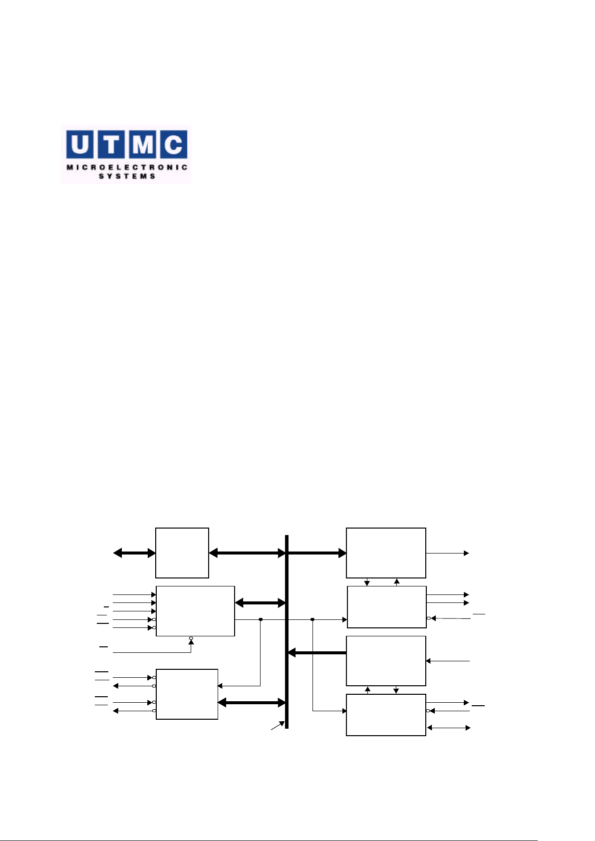
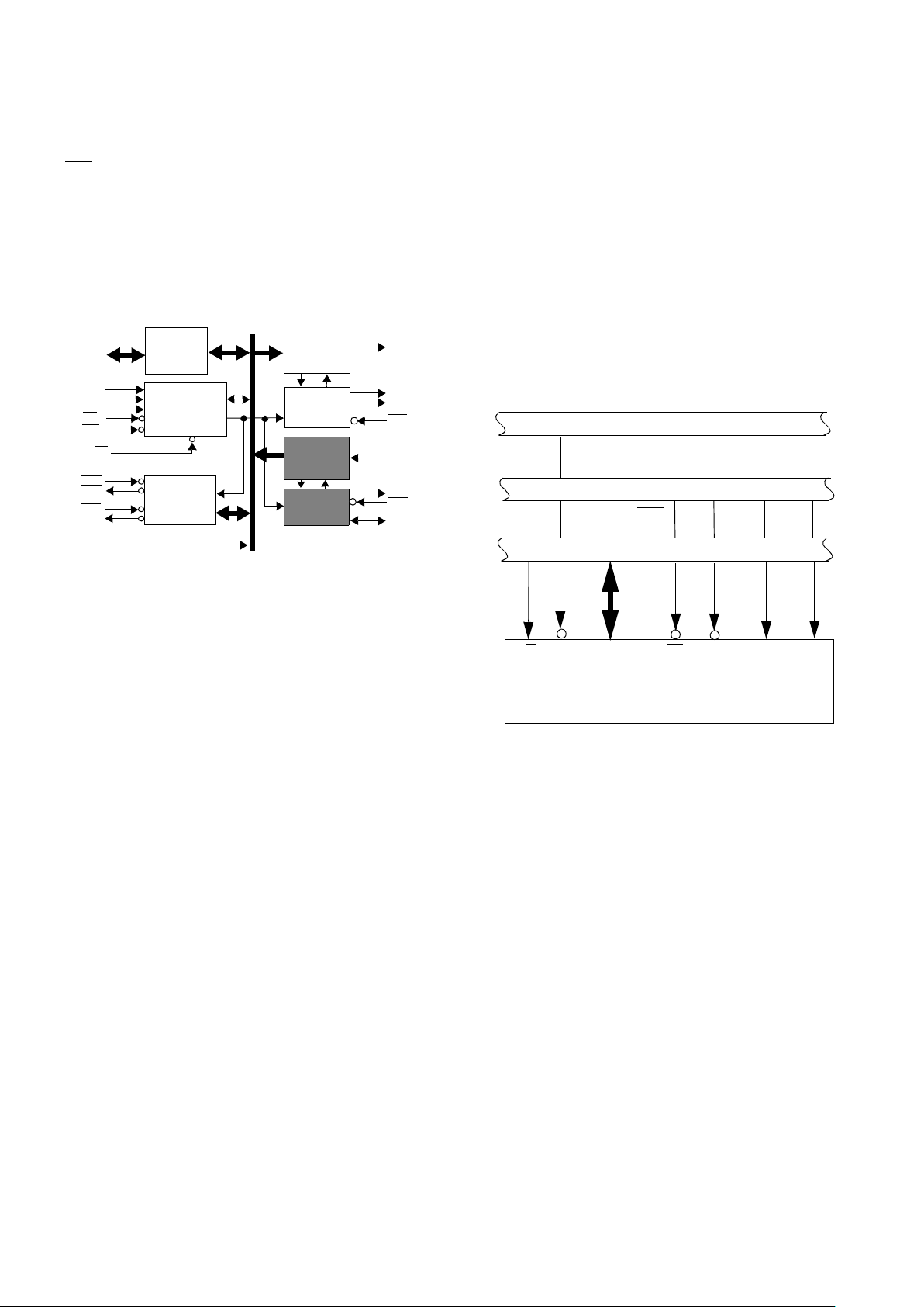
Figure 1. UT82CRH51A USART Block Diagram
D(7:0)
DATA
BUS
BUFFER
READ/WRITE
CONTROL
LOGIC
MODEM
CONTROL
TRANSMIT
BUFFER
(P-S)
TRANSMITTER
CONTROL
RECEIVE
BUFFER
(S-P)
RECEIVER
CONTROL
RESET
CLK
C/D
RD
WR
CS
DSR
DTR
CTS
RTS
TxRDY
TxEMPTY
TxC
TxD
RxD
RxRDY
RxC
SYNDET/
BRKDET
INTERNAL
DATA BUS
Standard Products
UT82CRH51A USART
Preliminary Data Sheet
December 9, 1999
Page 2
2
1.0 Functional Description
The UT82CRH51A is designed for a wide range of
microcomputers. Like other I/O devices in a microcomputer
system, its functional configuration is programmed by the
system’s software for maximum flexibility. The UT82CRH51A
can support most serial data techniques in use.
In a communication environment an interface device must
convert parallel format system data into serial format for
transmission and convert incoming serial format data into
parallel system data for reception. The interface device must also
delete or insert bits or characters that are functionally unique to
the communication technique. Therefore, the interface should
appear "transparent" to the CPU, a simple input or output of byteoriented system data (figure 7).
1.1 DATA BUS BUFFER
This three-state, bidirectional, 8-bit buffer is used to interface the
UT82CRH51A to the system Data Bus. Data is transmitted or
received by the buffer upon execution of INput or OUTput
instructions of the CPU. Control words, Command words and
Status information are also transferred through the Data Bus
Buffer. The Command Status, Data-In and Data-Out registers
are separate, 8-bit registers communicating with the system bus
through the Data Bus Buffer.
This functional block accepts inputs from the system Control bus
and generates control signals for overall device operation. It
contains the Control Word Register and Command Word
Register that store the various control formats for the device
functional definition.
1.2 READ/WRITE CONTROL LOGIC
1.2.1 RESET (Reset)
A "high" on this input forces the UT82CRH51A into an "Idle"
mode. The device remains at "Idle" until a new set of control
words is written into the UT82CRH51A to program its functional definition. Minimum RESET pulse width is 6tCY (clock must
be running).
A command reset operation also puts the device into the "Idle"
state.
1.2.2 CLK (CLOCK)
The CLK input is used to generate internal device timing and is
normally connected to the Phase 2 (TTL) output of the Clock
Generator. No external inputs or outputs are referenced to CLK,
but the frequency of CLK must be greater than 30 times the Receiver or Transmitter data bit rates.
1.2.3 WR (Write)
A "low" on this input informs the UT82CRH51A the CPU is
writing data or control words to the UT82CRH51A (figure 4).
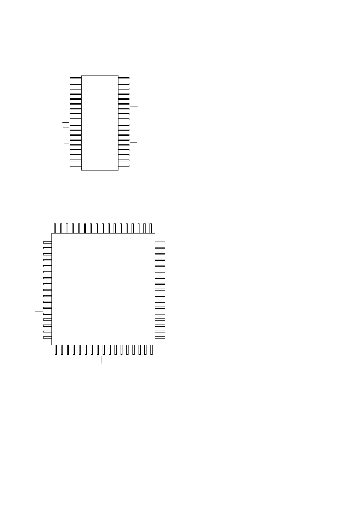
1 36
2 35
3 34
4 33
5 32
6 31
7 30
8 29
9 28
10 27
11 26
12 25
13 24
14 23
15 22
16 21
17 20
18 19
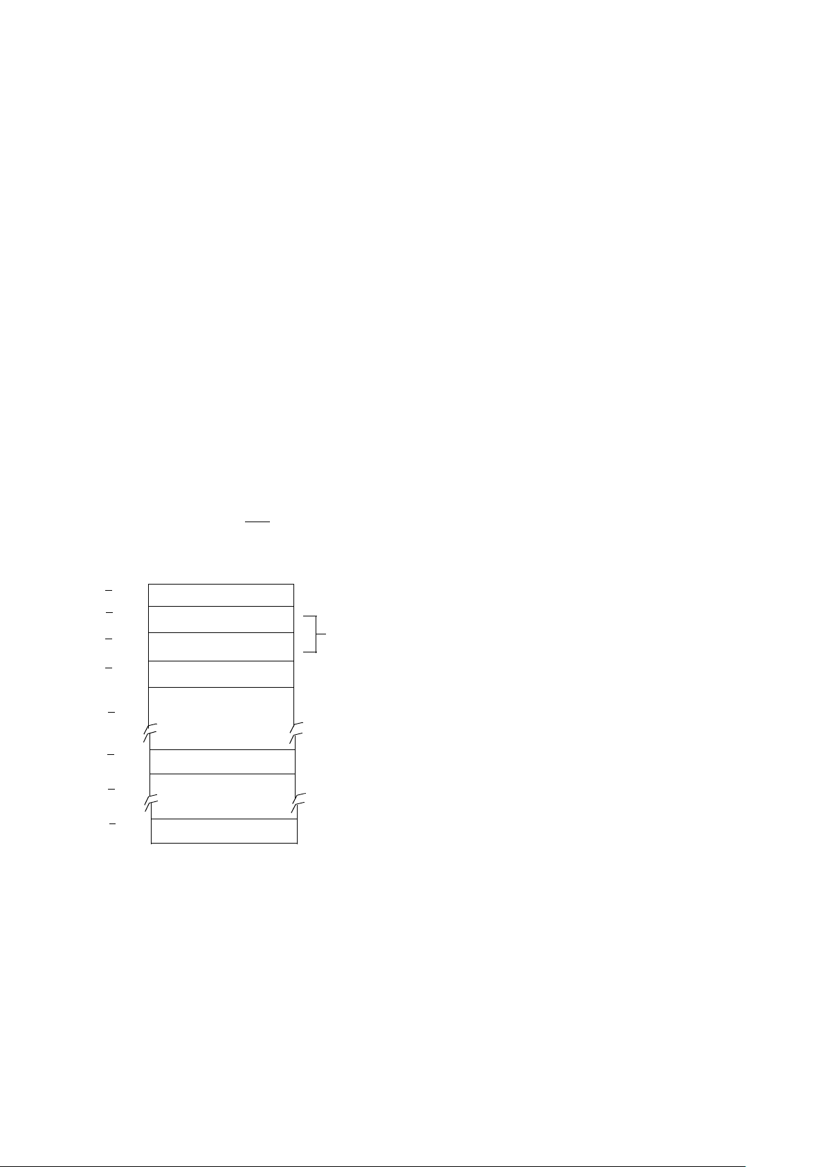
Figure 2. UT82CRH51A Pinout (36)
V
SS
V
DD
D2
D1
D0
RxC
DTR
RTS
DSR
RESET
CLK
TxD
TxEMPTY
CTS
SYNDET
TxRDY
V
DD
V
SS
V
SS
V
DD
RxD
D4
NC
NC
D5
D6
D7
TxC
WR
CS
C/D
RD
RxRDY
D3
V
DD
V
SS
9
8
7
6
5
4
3
2
1
68
67
66
65
64
63
62
61
44 45 46 47 48 49 50 51 52 53 54 55 56 57 58 59 60
27
28
29
30
31
32
33
34
35
36
37
38
39
40
41
42
43
26 25 24 23 22 21 20 19 18 17 16 15 14 13 12 11 10
Top View
NC
NC
V
SS
NC
RxD
NC
D3
NC
D2
NC
D1
NC
D0
NC
V
DD
NC
NC
NC
NC
C/D
NC
RD
NC
RxDY
NC
TxRDY
NC
SYNDET
NC
CTS
NC
TxE
NC
NC
NC
NC
D4
NC
D5
NC
D6
NC
D7
NC
TxC
NC
WR
NC
CS
NC
NC
NC
NC
TxD
NC
CLK
NC
RESET
NC
DSR
NC
RTS
NC
DTR
NC
RxC
NC
NC
Figure 3. UT82CRH51A Pinout (68)
Page 3
3
1.2.4 RD (Read)
A "low" on this input informs the UT82CRH51A the CPU is
reading data or status information from the UT82CRH51A (figure 4).
1.2.5 C/D (Control/Data)
This input, in conjunction with the WR and RD inputs, informs
the UT82CRH51A the word on the Data Bus is either a data
character, control word or status information.
1 = CONTROL/STATUS; 0 = DATA
1.2.6 CS (Chip Select)
A "low" on this input selects the UT82CRH51A. No reading or
writing will occur unless the device is selected. When CS is
high, the Data Bus is in the float state and RD and WR have no
effect on the chip.
1.3 MODEM CONTROL
The UT82CRH51A has a set of control inputs and outputs that
can be used to simplify the interface to almost any modem. The
modem control signals are general purpose in nature and can be
used to functions, other than modem control, if necessary (figure
5).
1.3.1 DSR (Data Set Ready)
The DSR input signal is a general-purpose, 1-bit inverting input
port. Its condition can be tested by the CPU using a Status Read
operation. The DSR input is normally used to test modem conditions such as Data Set Ready.
1.3.2 DTR (Data Terminal Ready)
The DTR output signal is a general-purpose, 1-bit inverting output port. It can be set "low" by programming the appropriate bit
in the Command Instruction word. The DTR output signal is
normally used for modem control such as Data Terminal Ready.
1.3.3 RTS (Request to Send)
The RTS output signal is a general-purpose, 1-bit inverting output port. It can be set "low" by programming the appropriate bit
in the Command Instruction word. The RTS output signal is
normally used for modem control such as Request to Send.
1.3.4 CTS (Clear to Send)
A "low" on this input enables the UT82CRH51A to transmit serial data if the TxEnable bit in the Command byte is set to a
"one". If either a TxEnable off or CTS off condition occurs
while the Tx is in operation, the Tx transmits all the data in the
USART written prior to TxDisable command before shutting
down.
1.4 TRANSMIT BUFFER
The Transmit Buffer Accepts parallel data from the Data Bus
Buffer, converts it to a serial bit stream, inserts the appropriate
characters or bits (based on the communication technique) and
outputs a composite serial stream of data on the TxD output pin
on the falling edge of TxC. The transmitter begins transmission
upon being enabled if CTS = 0. The TxD line will be held in the
marking state immediately upon a master Reset or when TxEnable or CTS is off or the transmitter is empty (figure 5).
1.5.TRANSMITTER CONTROL
The Transmitter Control manages all activities associated with
the transmission of serial data. It accepts and issues signals both
externally and internally to accomplish this function (figure 5).
1.5.1 TxRDY (Transmitter Ready)
This output signals the CPU the transmitter is ready to accept a
data character. The TxRDY output pin can be used as an interrupt to the system since it is masked by TxEnable; or, for Polled
operation, the CPU can check TxRDY using a Status Read operation. TxRDY is automatically reset by the leading edge of
WR when a data character is loaded from the CPU.
Note: When using the Polled operation, the TxRDY status bit
is not masked by TxEnable, but will only indicate the Empty/
Full Status of the Tx Data Input Register.
1.5.2 TxEMPTY (Transmitter Empty)
When the UT82CRH51A has no characters to send, the TxEMPTY output will go "high". It resets upon receiving a character
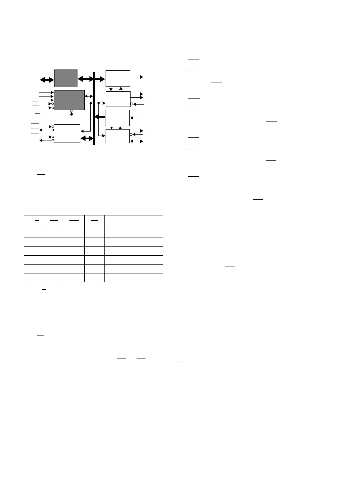
C/D RD WR CS
0 0 1 0
DATA -> DATA BUS
0 1 0 0
DATA BUS -> DATA
1 0 1 0
STATUS -> DATA BUS
1 1 0 0
DATA BUS -> CONTROL
X 1 1 0
DATA BUS -> 3-STATE
X X X 1
DATA BUS -> 3-STATE
Figure 4. UT82CRH51A Block Diagram Showing Data Bus Buffer
and Read/Write Logic Functions
D(7:0)
DATA
BUS
BUFFER
READ/WRITE
CONTROL
LOGIC
MODEM
CONTROL
TRANSMIT
BUFFER
(P-S)
TRANSMITTER
CONTROL
RECEIVE
BUFFER
(S-P)
RECEIVER
CONTROL
RESET
CLK
C/D
RD
WR
CS
DSR
DTR
CTS
RTS
TxRDY
TxEMPTY
TxC
TxD
RxD
RxRDY
RxC
SYNDET/
BRKDET
Page 4
4
from the CPU if the transmitter is enabled. TxEMPTY remains
low when the transmitter is disabled even if it is actually empty.
TxEMPTY can be used to indicate the end of a transmission
mode, so the CPU knows when to turn the line around in the
half-duplex operational mode.
In the Synchronous mode, a "high" on this output indicates that
a character has not been loaded and the SYNC character or characters are about to be or are being transmitted automatically as
"fillers". TxEMPTY does not go low when the SYNC characters are being shifted out.
1.5.3 TxC (Transmitter Clock)
The Transmitter Clock controls the rate at which the character is
to be transmitted. In the Synchronous transmission mode, the
Baud Rate (1x) is equal to the TxC frequency. In Asynchronous
transmission mode, the baud rate is a fraction of the actual TxC
frequency. A portion of the mode instruction selects this factor;
it can be 1, 1/16 or 1/64 the TxC.
For example:
If Baud Rate equals 110 Baud,
TxC equals 110 Hz in the 1x mode
TxC equals 1.72 kHz in the 16x mode
TxC equals 7.04 kHz in the 64x mode
The falling edge of TxC shifts the serial data out of the
UT82CRH51A.
1.6 RECEIVE BUFFER
The Receiver accepts serial data, converts this serial input to
parallel format, checks for bits or characters that are unique to
the communication technique and sends an "assembled" character to the CPU. Serial data is input to RxD pin, and is clocked
in on the rising edge of RxC (figure 6).
1.7 RECEIVER CONTROL
This functional block manages all receiver-related activities
which consists of the following features (figure 6).
• The RxD initialization circuit prevents the
UT82CRH51A from mistaking an unused input line for
an active low data line in the "break condition". Before
starting to receive serial characters on the RxD line, a
valid "1" must first be detected after a chip master Reset.
Once this has been determined, a search for a valid low
(Start bit) is enabled. This feature is only active in the
asynchronous mode, and is only done once for each master Reset.
• The False Start bit detection circuit prevents false starts
due to a transient noise spike by first detecting the falling
edge and then strobing the nominal center of the Start bit
(RxD = low).
• Parity error detection sets the corresponding status bit.
• The Framing Error status bit is set if the Stop bit is absent
at the end of the data byte (asynchronous mode).
1.7.1 RxRDY (Receiver Ready)
This output indicates the UT82CRH51A contains a character
ready to be input to the CPU. RxRDY can be connected to the
interrupt structure of the CPU or, for polled operation, the CPU
checks the condition of RxRDY using a Status Read operation.
RxEnable, when off, holds RxRDY in the Reset Condition. For
Asynchronous mode, to set RxRDY, the Receiver must be enabled to sense a Start Bit and a complete character must be assembled and transferred to the Data Output Register. For
Synchronous mode, to set RxRDY, the Receiver must be enabled and a character must finish assembly and be transferred to
the Data Output Register.
Failure to read the received character from the Rx Data Output
Register prior to the assembly of the next Rx Data character will
set overrun condition error and the previous character will be
written over and lost. If the Rx Data is being read by the CPU
when the internal transfer is occurring, overrun error will be set
and the old character will be lost.
1.7.2 RxC (Receiver Clock)
The Receiver Clock controls the rate at which the character is to
be received. In Synchronous Mode, the Baud Rate (1x) is equal
to the actual frequency of RxC. In Asynchronous Mode, the
Baud Rate is a fraction of the actual RxC frequency. A portion
of the mode instruction selects this factor: 1, 1/16 or 1/64 the
RxC.
For example:
Baud Rate Equals 300 Baud, if
RxC equals 300 Hz in the 1x mode
RxC equals 4800 Hz in the 16x mode
RxC equals 19.2 kHz in the 64x mode
Baude Rate equals 2400 Baude, if
RxC equals 2400 Hz in the 1x mode
RxC equals 38.4 kHz in the 16x mode
RxC equals 153.6 kHz in the 64x mode
Data is sampled into the UT82CRH51A on the rising edge of
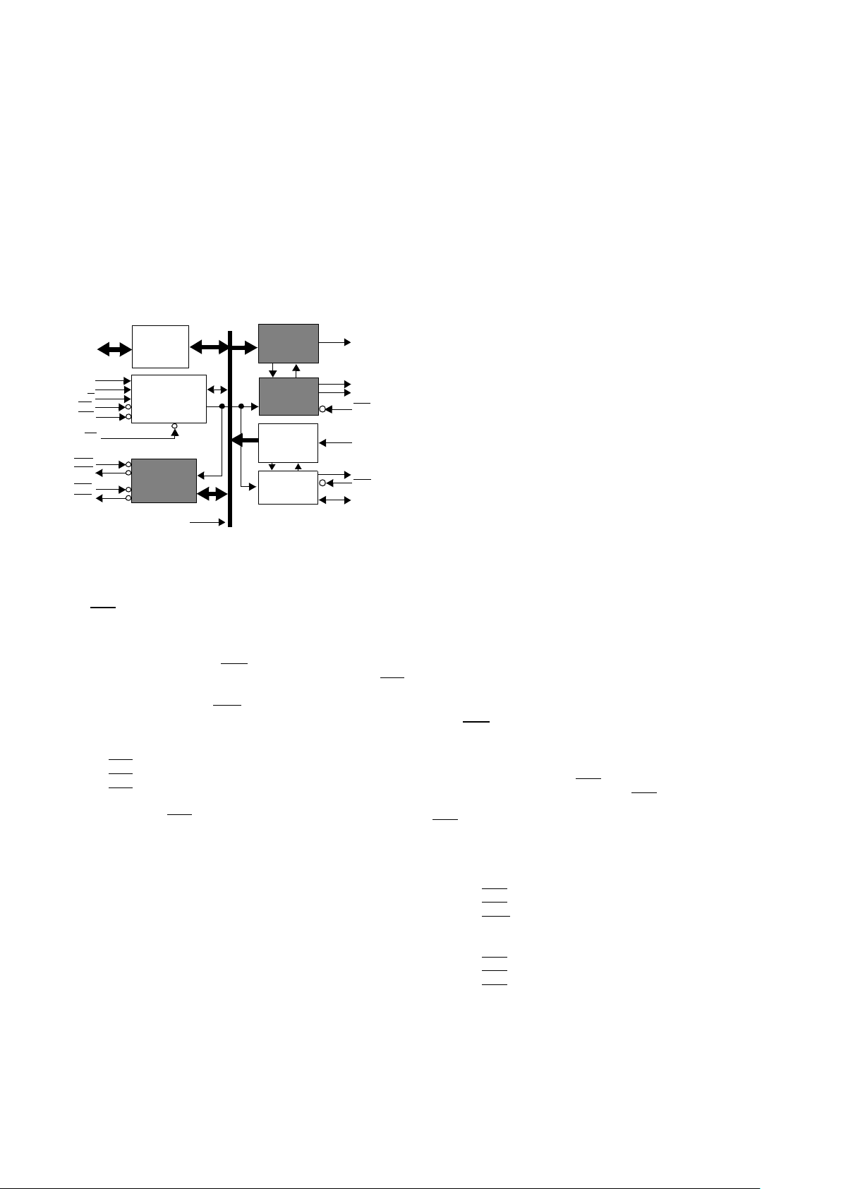
Figure 5. UT82CRH51A Block Diagram Showing Modem
and Transmitter Buffer and Control Functions
D(7:0)
DATA
BUS
BUFFER
READ/WRITE
CONTROL
LOGIC
MODEM
CONTROL
TRANSMIT
BUFFER
(P-S)
TRANS-
MITTER
CONTROL
RECEIVER
BUFFER
(S-P)
RECEIVER
CONTROL
RESET
CLK
C/D
RD
WR
CS
DSR
DTR
CTS
RTS
TxRDY
TxEMPTY
TxC
TxD
RxD
RxRDY
RxC
SYNDET/
BRKDET
INTERNAL
DATA BUS
Page 5
5
RxC.
NOTE: In most communications systems, the UT82CRH51A
handles both the transmission and reception operations of a single link. Consequently, the Receive and Transmit Baud Rates
will be the same. Both TxC and RxC requires identical frequencies for this operation and can be tied together and connected to
a single frequency source (Baud Rate Generator) to simplify the
interface.
1.7.3 SYNDET (SYNC Detect/BRKDET Break Detect)
This pin is used in Synchronous Mode for SYNDET and may be
used as either input or output programmable through the Control
Word. It is reset to output mode low upon RESET. When used
as an output (internal Sync mode), the SYNDET pin goes high
to indicate that the UT82CRH51A has located the SYNC character in the Receive mode. If the UT82CRH51A is programmed
to use double Sync characters (bisync), then SYNDET goes high
in the middle of the last bit of the second Sync character. SYNDET automatically resets upon a Status Read Operation.
When used as an input (external SYNC detect mode), a positive
going signal causes the UT82CRH51A to start assembling data
characters on the rising edge of the next RxC. Once in SYNC,
the "high" input signal can be removed. When External SYNC
Detect is programmed, Internal SYNC Detect is disabled.
1.7.4 BREAK (Async Mode Only)
This output goes high whenever the receiver remains low
through two consecutive stop bit sequences (including the start
bits, data bits, and parity bits). Break Detect may also be read
as a Status bit. It is reset only upon a master chip Reset or Rx
Data returning to a "one" state.
Figure 6. UT82CRH51A Block Diagram Showing
Receiver Buffer and Control Functions
D(7:0)
DATA
BUS
BUFFER
READ/WRITE
CONTROL
LOGIC
MODEM
CONTROL
TRANSMIT
BUFFER
(P-S)
TRANS-
MITTER
CONTROL
RECEIVER
BUFFER
(S-P)
RECEIVER
CONTROL
RESET
CLK
C/D
RD
WR
CS
DSR
DTR
CTS
RTS
TxRDY
TxEMPTY
TxC
TxD
RxD
RxRDY
RxC
SYNDET/
BRKDET
INTERNAL
DATA BUS
CONTROL BUS
ADDRESS BUS
DATA BUS
UT82CRH51A
C/D
CS
D7-D
0
RD
WR
CLKRESET
A
0
I/O R I/O W
RESET
0
2
(TTL)
8
Figure 7. UT82CRH51A Interface to Standard
System Bus
Page 6
6
2.0 DETAILED OPERATION DESCRIPTION
2.1 General
The complete functional definition of the UT82CRH51A is programmed by the system’s software. A set of control words must
be sent out by the CPU to initialize the UT82CRH51A to support the desired communications format. These control words
will program the: BAUD RATE, CHARACTER LENGTH,
NUMBER OF STOP BITS, SYNCHRONOUS or ASYNCHRONOUS OPERATION, EVEN/ODD/OFF PARITY, etc.
In the Synchronous Mode, options are also provided to select either internal or external character synchronization (figure 8).
Once programmed, the UT82CRH51A is ready to perform its
communication functions. The TxRDY output is raised "high"
to signal the CPU the UT82CRH51A is ready to receive a data
character from the CPU. This output (TxRDY) is reset automatically when the CPU writes a character into the UT82CRH51A.
On the other hand, the UT82CRH51A receives serial data from
the MODEM or I/O device. Upon receiving an entire character,
the RxRDY output is raised "high" to signal the CPU the
UT82CRH51A has completed character ready for the CPU to
fetch. RxRDY is reset automatically upon the CPU data read
operation.
The UT82CRH51A cannot begin transmission until the TxEnable (Transmitter Enable) bit is set in the Command Instruction
and it has received a Clear to Send (CTS) input. The TxD output
is held in the marking state upon Reset.
2.2 Programming the UT82CRH51A
Prior to starting data transmission or reception, the
UT82CRH51A must be loaded with a set of control words generated by the CPU. These control signals define the complete
functional definition of the UT82CRH51A and must immediately follow a Reset operation (internal or external).
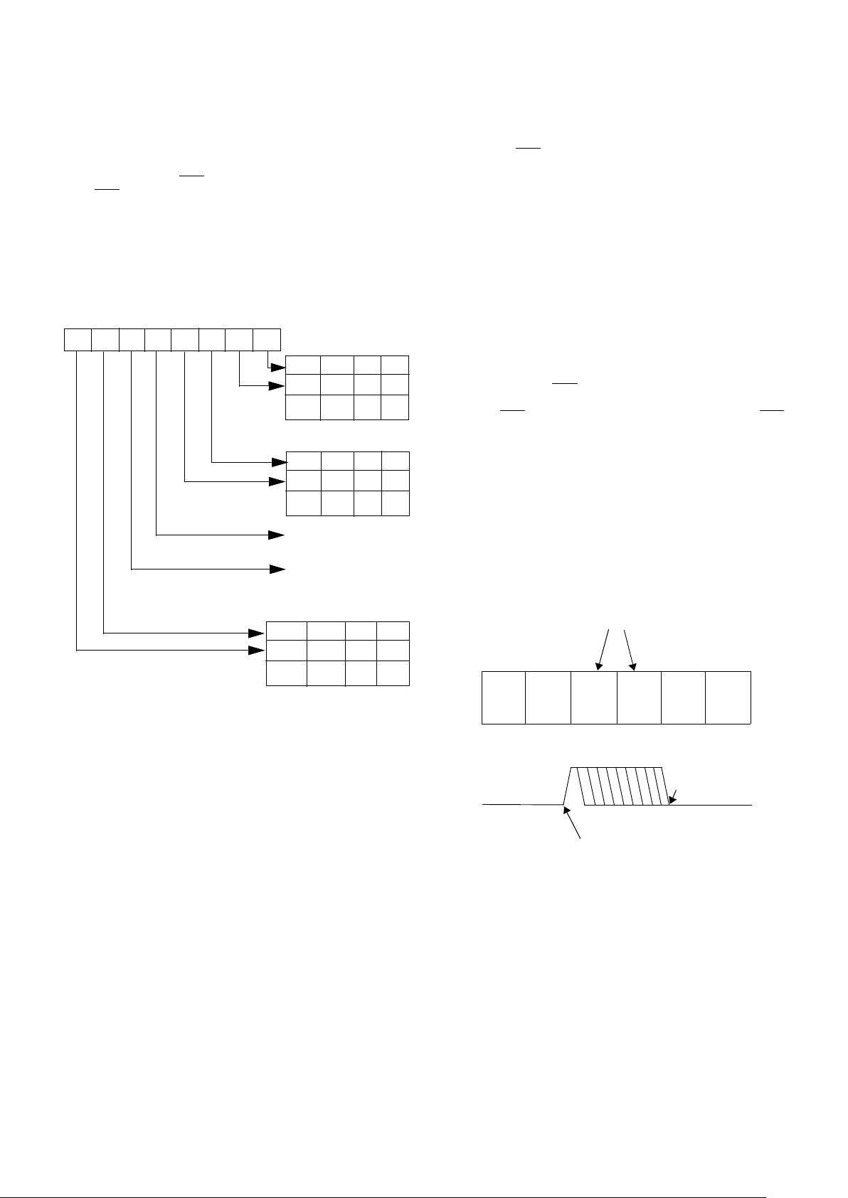
The control words are split into two formats:
1. Mode Instruction
2. Command Instruction
2.2.1 Mode Instruction
This instruction defines the general operational characteristics
of the UT82CRH51A. It must follow a Reset operation (internal
or external), once the Mode Instruction has been written into the
UT92CRH51A by the CPU, SYNC characters or Command Instructions (figure 8).
2.2.2 Command Instruction
This instruction defines a word that is used to control the actual
operation of the UT82CRH51A.
Both the Mode and Command Instructions must conform to a
specified sequence for proper device operation (see Figure 8).
The Mode Instruction must be written immediately following a
Reset operation prior to using the UT82CRH51A for data communication.
All control words written into the UT82CRH51A after the Mode
Instruction loads the Command Instruction. Command Instructions can be written into the UT82CRH51A at any time in the
data block during the operation of the UT82CRH51A. To return
to the Mode Instruction format, the master Reset bit in the Command Instruction word can be set to initiate an internal Reset operation which automatically places the UT82CRH51A back into
the Mode Instruction format. Command Instructions must follow the Mode Instructions or Sync characters.
2.2.3 Mode Instruction Definition
The UT82CRH51A can be used for either Asynchronous or
Synchronous data communication. To understand how the
Mode Instruction defines the functional operation of the
UT82CRH51A, the designer views the device as two separate
components, one Asynchronous and the other Synchronous,
sharing the same package. The format definition can be
changed only after a master chip Reset. For explanation purposes the two formats will be isolated.
NOTE: When parity is enabled it is not considered as one of the
data bits for the purpose of programming the word length. The
actual parity bit received on the Rx Data line cannot be read on
the Data bus. In the case of a programmed character length of
less than 8 bits, the least significant Data Bus bits holds the data;
unused bits are "don’t care" when writing data to the
UT82CRH51A and will be "zeroes" when reading the data from
the UT82CRH51A.
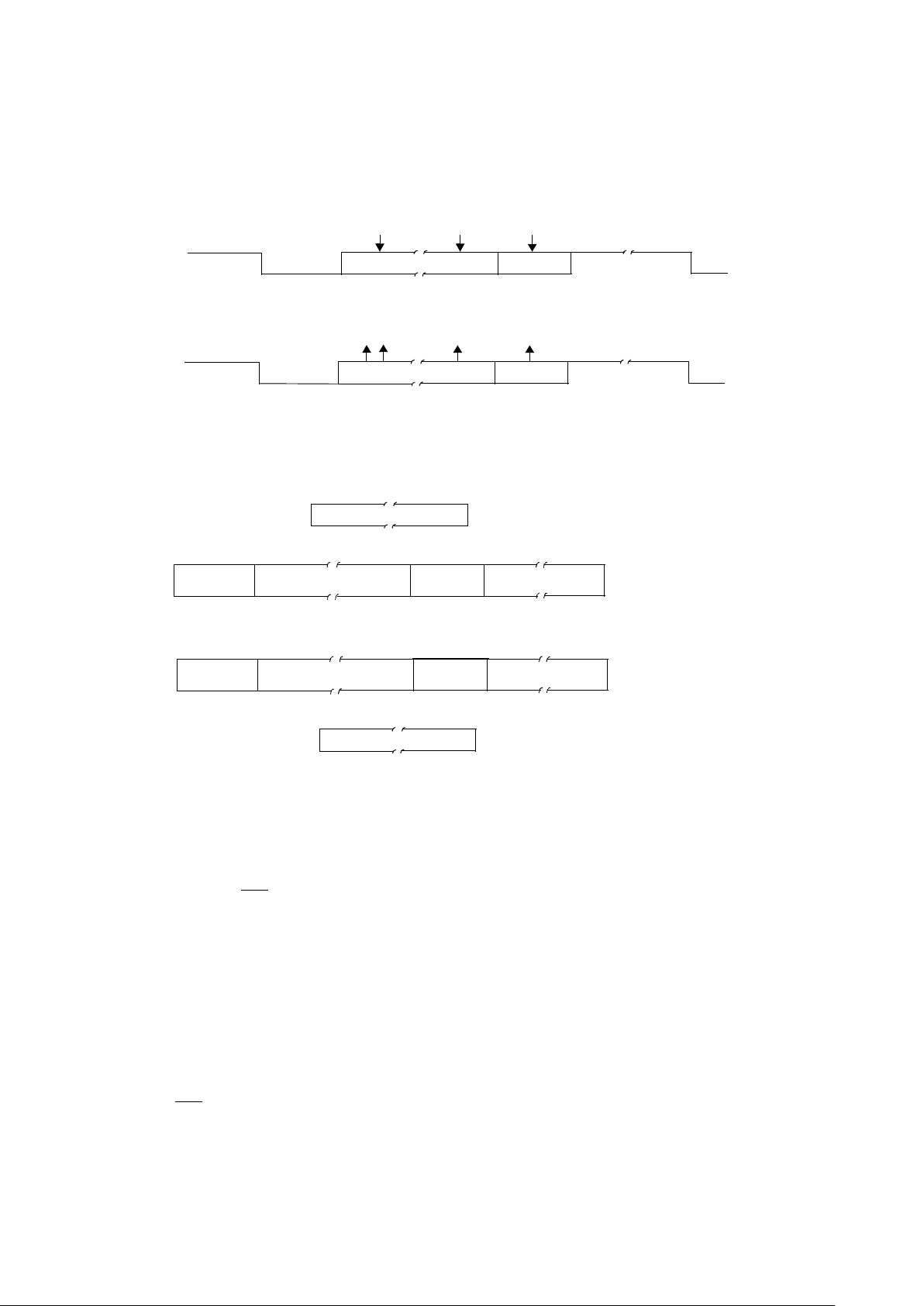
2.2.4 Asynchronous Mode (Transmission)
Whenever a data character is sent by the CPU the
UT82CRH51A automatically adds a Start bit (low level) followed by the data bits (least significant bit first), and the programmed number of Stop bits to each character. Also, an even
or odd Parity bit is inserted prior to the Stop bit(s) as defined by
MODE INSTRUCTION
SYNC CHARACTER 1
SYNC CHARACTER 2
COMMAND INSTRUCTION
DATA
DATA
COMMAND INSTRUCTION
COMMAND INSTRUCTION
C/D = 1
C/D = 1
C/D = 1
C/D = 1
C/D = 0
C/D = 1
C/D = 0
C/D = 1
SYNC
MODE
ONLY*
NOTE: The second SYNC character is skipped if MODE instruction has programmed
the UT82CRH51A to single character internal SYNC Mode. Both SYNC characters are
skipped if MODE instruction has programmed the UT82CRH51A to ASYNC mode or
External SYNC mode.
Figure 8. Typical Data Block
Page 7
7
the Mode Instruction. The character is then transmitted as a serial data stream on the TxD output. The serial data is shifted out
on the falling edge of TxC at a rate equal to 1, 1/16, or 1/64 that
of the TxC as defined by the Mode Instruction. BREAK characters can be continuously sent to the TxD if commanded to do
so.
When no data characters have been loaded into the
UT82CRH51A the TxD output remains "high" (marking) unless
a Break (continuously low) has been programmed (figure 9).
2.2.5 Asynchronous Mode (Receive)
The RxD line is normally high. A falling edge on this line triggers the beginning of a START bit. The validity of this START
bit is checked by again strobing this bit at its nominal center
(16x or 64x mode only). If a low is detected again, it is a valid
START bit, and the bit counter starts counting. The bit counter
thus locates the center of the data bits, the parity bit (if it exists),
and the stop bits. If parity error occurs, the parity error flag is
set. Data and parity bits are sampled on the RxD pin with the
rising edge of RxC. If a low level is detected as the STOP bit,
the Framing Error flag sets. The STOP bit signals the end of a
character. Note: The receiver requires only one stop bit regard-
less of the number of stop bits programmed. This character is
then loaded into the parallel I/O buffer of the UT82CRH51A.
The RxRDY pin is raised to signal the CPU that a character is
ready to be fetched. If a previous character has not been fetched
by the CPU, the present character replaces it in the I/O buffer,
and the OVERRUN Error flag is raised (thus the previous character is lost). All of the error flags can be reset by an Error Reset
Instruction. The occurrence of any of these errors will not affect
the operation of the UT82CRH51A (figure 10).
2.2.6 Synchronous Mode (Transmission)
The TxD output is continuously high until the CPU sends its
first character to the UT82CRH51A which usually is a SYNC
character. When the CTS line goes low, the first character is serially transmitted out. All characters are shifted out on the falling edge of TxC. Data is shifted out at the same rate as the TxC.
Once transmission has started, the data stream at TxD output
continues at the TxC rate. If the CPU does not provide the
UT82CRH51A with a data character before the UT82CRH51A
Transmitter Buffers become empty, the SYNC characters (or
character if in single SYNC character mode) will be automatically inserted in the TxD data stream. In this case, the TxEMPTY pin is raised high to signal that the UT82CRH51A is empty
and SYNC characters are being sent out. TxEMPTY does not
go low when the SYNC is being shifted out (see figure 11). The
TxEMPTY pin is internally reset by a data character being written into the UT82CRH51A.
S2S
1
EP
PEN
L
2L1
B
2
B
1
D
5
D
6
D
7
D4D3D
2
D1D
0
0
SYNC
MODE
0
1
(1X)
0
0
(16X)
1
1
1
(64X)
BAUD RATE FACTOR
0
5
BITS
0
1
6
BITS
0
0
7
BITS
1
1
1
8
BITS
CHARACTER LENGTH
PARITY ENABLE
1 = ENABLE 0 = DISABLE
EVEN PARITY
GENERATION/CHECK
1 = EVEN 0= ODD
0
INVALID
0
1
1
BITS
0
0
1 1/2
BITS
1
1
1
2
BITS
NUMBER OF STOP BITS
(ONLY AFFECTS Tx:Rx
NEVER REQUIRES MORE
THAN ONE STOP BIT)
Figure 9. Mode and Command Instruction Format,
Asynchronous Node
S2S
1
EP
PEN
L
2L1
B
2
B
1
D
5
D
6
D
7
D4D3D
2
D1D
0
0
SYNC
MODE
0
1
(1X)
0
0
(16X)
1
1
1
(64X)
BAUD RATE FACTOR
0
5
BITS
0
1
6
BITS
0
0
7
BITS
1
1
1
8
BITS
CHARACTER LENGTH
PARITY ENABLE
1 = ENABLE 0 = DISABLE
0
INVALID
0
1
1
BITS
0
0
1 1/2
BITS
1
1
1
2
BITS
NUMBER OF STOP BITS
Figure 11. Synchronous Mode
DATA
DATA
SYNC 1 SYNC 2
DATA
- - - - - -
TxD
AUTOMATICALLY INSERTED BY USART
TxEMPTY
NOMINAL CENTER OF LAST BIT
FALLS UPON CPU
WRITING A
CHARACTER TO
THE USART
Page 8
8
2.2.7 Synchronous Mode (Receive)
In this mode, character synchronization can be internally or externally achieved. If the SYNC mode has been programmed, an
ENTER HUNT command should be included in the first command instruction word written. Data on the RxD pin is then
sampled on the rising edge of RxC. The content of the Rx buffer
is compared at every bit boundary with the first SYNC character
until a match occurs. If the UT82CRH51A has been programmed for two SYNC characters, the subsequent received
character is also compared; when both SYNC characters have
been detected, the USART ends the HUNT mode and is in character synchronization. The SYNDET pin is then set high and is
reset automatically by a STATUS READ. If parity is programmed, SYNDET will not be set until the middle of the parity
bit instead of the middle of the last data bit.
In the external SYNC mode, synchronization is achieved by applying a high level of the SYNDET pin, thus forcing the
UT82CRH51A out of the HUNT mode. The high level can be
removed after one RxC cycle. An ENTER HUNT command has
no effect in the asynchronous mode of operation.
Parity error and overrun error are both checked in the same way
as in the Asynchronous Rx mode. Parity is checked when not in
HUNT, regardless of whether the Receiver is enabled or not
(Figure 12).
The CPU can command the receiver to enter the HUNT mode if
synchronization is lost. This will also set all the used character
bits in the buffer to a "one", thus preventing a possible false
SYNDET caused by data that happens to be in the Rx Buffer at
ENTER HUNT time. Note: The SYNDET F/F is reset at each
Status Read regardless of whether internal or external sync has
been programmed. This does not cause the UT82CRH51A to
return to the HUNT mode. When the SYNC mode but not in
HUNT, Sync Detection is still functional, but only occurs at the
"known" word boundaries. Thus, if one Status Read indicates
SYNDET and a second Status Read also indicates SYNDET,
then the programmed SYNDET characters have been received
since the previous Status Read. (If double character sync has
been programmed, then both sync characters have been contiguously received to gate a SYNDET indication.) When external
SYNDET mode is selected, internal Sync Detection is disabled,
and the SYNDET F/F may be set at any bit boundary (figure 13).
TRANSMITTER OUTPUT
START
BIT
DATA BITS
PARITY BITS
STOP BITS
D0 D1 --------------D
x
Generated by
UT82CRH51A
MARKING
TxD
RECEIVER INPUT
START
BIT
DATA BITS
PARITY BITS
STOP BITS
D0 D1 --------------D
x
DOES NOT APPEAR ON
THE DATA BUS
RxD
PROGRAMMED CHARACTER
LENGTH
TRANSMISSION FORMAT
DATA CHARACTER
CPU BYTE (5-8 BITS/CHAR)
START
BIT
DATA CHARACTER
PARITY BITS
STOP BITS
ASSEMBLED SERIAL DATA OUTPUT (TxD)
START
BIT
DATA CHARACTER
PARITY BITS
STOP BITS
SERIAL DATA INPUT (RxD)
RECEIVE FORMAT
DATA CHARACTER
CPU BYTE (5-8 BITS/CHAR)
*Note: If character length is defined
as 5,6 or 7 bits, the unused bits are
set to "ZERO"
Figure 10. Asynchronous Mode
}
Page 9

9
3.0 COMMAND INSTRUCTION DEFINITION
Once the functional definition of the UT82CRH51A has been
programmed by the Mode Instruction and the sync characters
are loaded (if in Sync Mode) then the device is ready to be used
for data communication. The Command Instruction controls the
actual operation of the selected format. Functions such as Enable Transmit/Receive, Error Reset and Modem Controls are
provided by the Command Instruction.
Once the Mode Instruction has been written into the
UT82CRH51A and the Sync characters inserted, if necessary,
then all further "control write" (C/D = 1) will load a Command
Instruction. A Reset Operation (internal or external) returns the
UT82CRH51A to the Mode Instruction format. Note: Internal
Reset on Power-Up
When power is first applied, the UT82CRH51A may come up in
the Mode, Sync character or Command format. To guarantee
that the device is in the Command Instruction format before the
Reset command is issued, it is safest to execute the worst-case
initialization sequence (sync mode with two sync characters).
Loading three 00Hs consecutively into the device with C/D = 1
configures sync operation and writes two dummy 00H sync
characters. An Internal Reset command (40H) may then be issued to return the device to the "Idle" state (figure 14).
D
5
D
6
D4D3D2D1D
0
0
5
BIT
0
1
6
BITS
0
0
7
BITS
1
1
1
8
BITS
CHARACTER LENGTH
PARITY ENABLE
1 = ENABLE
0 = DISABLE
EVEN PARITY
GENERATION/CHECK
1 = EVEN 0= ODD
EXTERNAL SYNC DETECT
1 = SYNDET IS AN INPUT
0 = SYNDET IS AN OUTPUT
SCS
ES
D
EP
PE
N
L
2
L
1
0
0
D
7
Figure 12. Mode Instruction Format, Synchronous Mode
SINGLE CHARACTER SYNC
1 = SYNGLE SYNC
CHARACTER
0 = DOUBLE SYNC
CHARACTER
DATA CHARACTER
CPU BYTE (5-8 BITS/CHAR)
SYNC
CHAR 2
DATA CHARACTER
ASSEMBLED SERIAL DATA OUTPUT
(TxD)
SYNC
CHAR 1
RECEIVE FORMAT
DATA CHARACTER
CPU BYTE (5-8 BITS/CHAR)
SYNC
CHAR 2
DATA CHARACTER
ASSEMBLED SERIAL DATA OUTPUT
(RxD)
SYNC
CHAR 1
Figure 13. Data Format, Synchronous Mode
D
5
D
6
D4D3D2D1D
0
TRANSMIT ENABLE
1 = enable
0 = disable
DATA TERMINAL
READY
"high" will force DTR out-
put to zero
RECEIVE ENABLE
1 = enable
0 = disable
SEND BREAK CHARACTER
1 = forces TxD "low"
0 = normal operation
EH
IR
RTS
ER
SBR
RxE
DT
TxE
D
7
Figure 14. Mode Instruction Format,
Synchronous Mode
ERROR RESET
1 = reset error flags PE, OE, FE
REQUEST TO SEND
"high" will for RTS output to zero
INTERNAL RESET
"high" returns UT82CRH51A to
Mode Instruction Format
ENTER HUNT MODE
1 = enable search for Sync
Characters
Note: Error Reset must be performed whenever RxEnable
and Enter Hunt are programmed.
Page 10

10
4.0 STATUS READ DEFINITION
In data communication systems it is often necessary to examine
the "status" of the active device to ascertain if errors have occurred or other conditions requiring the processor’s attention.
The UT82CRH51A has facilities that allow the programmer to
"read" the status of the device at any time during the functional
operation. (Status update is inhibited during status read.)
A normal "read" command is issued by the CPU with C/D = 1 to
accomplish this function.
Some of the bits in the Status Read Format have identical meanings to external output pins to that the UT82CRH51A can be
used in a completely polled or interrupt-driven environment.
TxRDY is an exception (figure 15).
Note: Status update can have a maximum delay of 28 clock periods from the actual event affecting the status.
D
5
D
6
D
4
D3D
2
D1D
0
PARITY ERROR
The PE flag is set when a parity error
is detected. It is reset by the ER bit of
the Command Instruction. PE does
not inhibit operation of the
UT82CRH51A
OVERRUN ERROR
The OE flag is set when the CPU
does not read a character before the
next one becomes available. It is re-
set by the ER bit of the Command
Instruction. OE does not inhibit op-
eration of the UT82CRH51A how-
ever, the previously overrun
character is lost.
FRAMING ERROR (Async only)
The FE flag is set when a valid Stop
bit is not detected at the end of every
character. It is reset by the ER bit of
the Command Instruction. FE does
not inhibit the operation of the
UT82CRH51A
DSR
SYNDET/
FE
OE
PE Tx-
EMP-
RxR
DY
TxRD
Y
D
7
Note 1
SAME DEFINITION AS I/O PINS
DATA SET READY
Indicates that the DSR is at a zero
level.
Note : TxRDY status bit has different meanings from the TxRDY output pin.
The former is not conditioned by CTS and TxEN; the latter is conditioned by
both CTS and TxEN.
i.e TxRDY status bit = DB Buffer Empty
TxRDY pin out = DB Buffer Empty + (CTS-0) + (TxEN-1)
Figure 15. Status Read Format
Page 11

11
5.0 APPLICATIONS OF THE UT82CRH51A
Figures 16 thru 19 are examples of UT82CRH51A application
environments.
CONTROL BUS
ADDRESS BUS
DATA BUS
UT82CRH51A
8
RxD
TxD
RxC
TxC
EIA TO
TTL CON-
VERT
(OPT)
BAUD RATE
GENERATOR
CRT
TERMINAL
Figure 16. Asynchronous Serial Interface to CRT
Terminal, DC-9600 Baud
CONTROL BUS
ADDRESS BUS
DATA BUS
UT82CRH51A
8
RxD
TxD
RxC
TxC
SYNCHRONOUS
TERMINAL OR
PERIPHERAL
DEVICE
Figure 17. Synchronous Interface to Terminal, or
Peripheral Device
SYNDET
Page 12

12
CONTROL BUS
ADDRESS BUS
DATA BUS
UT82CRH51A
8
RxD
TxD
DSR
DTR
BUS TRANSCEIVER
Figure 18. Asynchronous Interface to Serial Bus
CTS
RTS
TxC
TxC
BAUD RATE
GENERATOR
SERIAL BUS
CONTROL BUS
ADDRESS BUS
DATA BUS
UT82CRH51A
8
RxD
TxD
RxC
TxC
BUS TRANSCEIVER
Figure 19. Synchronous Interface to Serial Bus
SYNDET
CTS
DSR
DTR
SERIAL BUS
RTS
Page 13

13
RADIATION HARDNESS SPECIFICATIONS
1
Notes:
1. Logic will not latchup during radiation exposure within the limits defined in the table.
2. Not tested, inherent of CMOS technology.
ABSOLUTE MAXIMUM RATINGS
1
Note:
1. Stresses outside the listed absolute maximum ratings may cause permanent damage to the device. This is a stress rating only, functional operation of the device at
these or any other conditions beyond limits indicated in the operational sections is not recommended. Exposure to absolute maximum rating conditions for extended
periods may affect device reliability and performance.
PARAMETER LIMIT UNITS
Total Dose 300 krad(Si)
SEL Latchup >120
MeV-cm2/mg
Neutron Fluence
2
1.0E14
n/cm
2
SYMBOL PARAMETER LIMIT (Mil only) UNITS
V
I/O
Voltage any pin -.5 to +7 V
T
STG
Storage Temperature range -65 to +150 °C
T
J
Maximum junction temperature +175 °C
P
D
Maximum power dissipation 1 W
Page 14

14
6.0 DC ELECTRICAL CHARACTERISTICS (Pre/Post-Radiation)*
V
DD
= 5.0V ± 10%; TA = -55°C to 125°C, GND = 0V)
Notes:
* Post-radiation performance guaranteed at 25°C per MIL-STD-883.
SYMBOL PARAMETER CONDITION MINIMUM MAXIMUM UNIT
V
IL
Low-level Input Voltage -0.5 0.8 V
V
IH
High-level Input Voltage 2.2 V
CC
V
V
OL
Low-level Output Voltage IOL = 2.2mA 0.45 V
V
OH
High-level Output Voltage IOH = -400µA 2.4 V
I
OFL
Output Float Leakage V
OUT
= VCC to 0.45V +10 µA
I
IL
Input Leakage VIN = VCC to 0.45V +10 µA
I
CC
Power Supply Current All Outputs = High 100 mA
C
IN
Input Capacitance fc = 1MHz 10 pF
C
I/O
I/O Capacitance Unmeasured pins returned to
GND
20 pF
Page 15

15
7.0 AC CHARACTERISTICS (Post-Radiation)
(V
DD
= 5.0V ± 5%; TA = -55°C to 125°C, GND = 0V)
SYMBOL PARAMETER MINIMUM MAXIMUM UNIT
t
CY
Clock Period
1,2
200 - ns
t
CLK
Clock High Pulse Width 100 - ns
t
CLK
Clock Low Pulse Width 100 ns
tR, t
F
Clock Rise and Fall Time 20 ns
t
DTx
TxD Delay from Falling Edge of TxC 1 µs
f
Tx
Transmitter Input Clock Frequency
1x Baud Rate
16x Baud Rate
64x Baud Rate
1
1
1
64
310
615
kHz
t
TPW
Transmitter Input Clock Pulse Width
1x Baud Rate
16x and 64x Baud Rate
12
1
t
CY
t
TPD
Transmitter Input Clock Pulse Delay
1x Baud Rate
16x and 64x Baud Rate
15
3
t
CY
f
Rx
Receiver Input Clock Frequency
1x Baud Rate
16x Baude Rate
64x Baude Rate
1
1
1
64
310
615
kHz
t
RPW
Receiver Input Clock Pulse Width
1x Baude Rate
16x and 64x Baude Rate
12
1
t
CY
t
RPD
Receiver Input Clock Pulse Width
1x Baude Rate
16x and 64x Baude Rate
15
3
t
CY
t
TxRDY TxRDY Pin Delay from End of Last Bit
3
35 ns
t
TxRDY CLEAR
TxRDY falling from Leading Edge of WR
3
50 ns
t
RxRDY
RxRDY Pin Delay from Center of Last Bit
3
26 t
CY
t
RxRDY CLEAR
RxRDY falling from Leading Edge of RD
3
400 ns
t
IS
Internal SYNDET Delay from Rising Edge of
RxC
3
26 t
CY
t
ES
External SYNDET Set-Up Time After Rising
Edge of RxC
3
18 t
CY
t
TxEMPTY
4
TxEMPTY Delay from Center of Last Bit
3
20 - t
CY
t
WC
4
Control Delay from Rising Edge of WRITE
(TxEn, DTR, RTS)
3
8 - t
CY
t
CR
4
Control to READ Set-Up Time (DSR, CTS)
3
20 - t
CY
Page 16

16
Note:
* Post-radiation performance guaranteed at 25°C per MIL-STD-883 Method 1019 at 300 krad(Si).
1. The TxC and RxC frequencies have the following limitations with respect to CLK: For 1x Vaude Rate, fTx or fRX < 1/(30 tCY). For 16x and 64x Baud Rate, fTx
or fRx < 1/(4.5 tCY).
2. Rest Pulse Width = 6 t
CY
minimum. System Clock must be running during Reset.
3. Status update can have a maximum delay of 28 clock periods from the event affecting the status.
4. Guaranteed by simulation, not tested.
AC CHARACTERISTICS READ CYCLE (Post-Radiation)
1
(V
DD
= 5.0V ± 5%; TA = -55°C to 125°C, GND = 0V)
Note:
* Post-radiation performance guaranteed at 25°C per MIL-STD-883 Method 1019 at 300 krad(Si).
1. AC timing measured VOH = 2.0, VOL = 0.8.
2. Chip Select (CS) and Command/Data (C/D) are considered as addresses.
3. Assumes that address is valid beroe READ falling.
4. Guaranteed by simulation, not tested.
AC CHARACTERISTICS WRITE CYCLE (Post-Radiation)
1
(V
DD
= 5.0V ± 5%; TA = -55°C to 125°C, GND = 0V)
Note:
* Post-radiation performance guaranteed at 25°C per MIL-STD-883 Method 1019 at 300 krad(Si).
1. AC timing measured VOH = 2.0, VOL = 0.8.
2. This recovery time is for Mode Initialization only. Write data is allowed only when TxRDY = 1. Recovery time between writes for Asynchronous Mode is 8 tCY
and for Synchronous Mode is 16 tCY.
3. Guaranteed by simulation, not tested.
SYMBOL PARAMETER MINIMUM MAXIMUM UNIT
t
AR
4
Address Stable Before READ (CS, C/D)
2
0 - ns
t
RA
4
Address Hold Time for READ (CS, C/D)
2
0 - ns
t
RR
4
READ Pulse Width 20 - ns
t
RD Data Delay from READ
3
CL = 150 pF
- 30 ns
t
DF
READ to Data Floating 1.8 45 ns
SYMBOL PARAMETER MINIMUM MAXIMUM UNIT
t
AW
3
Address Stable Before WRITE 0 - ns
t
WA
3
Address Hold Time for WRITE 0 - ns
t
WW
3
WRITE Pulse Width 20 - ns
t
DW
3
Data Delay from WRITE 15 - ns
t
WD
3
Data Hold Time for WRITE 5 - ns
t
RV
3
Recovery Time Between Writes
2
6 - t
CY
Page 17

17
t
CY
t
CLK
t
CLK
CLOCKφ
t
F
t
R
Figure 20. SYS CLOCK
t
DTx
t
DTx
t
TPD
t
TPW
TxC (1x Mode)
TxC (16x Mode)
Tx Data
Figure 21. Tx CLOCK And DATA
Start Bit Data Bit Data Bit
3t
CY
t
CLK
3t
CY
16 RxC PERIODS (16x MODE)
8 RxC PERIODS (16x MODE)
t
RPD
t
RPW
(Rx BAUD COUNTER STARTS HERE)
Rx Data
RxC (1x Mode)
RxC (16x Mode)
INT SAMPLING PULSE
Figure 22. Rx CLOCK And DATA
Page 18

18
Don't Care
Data Valid
Don't Care
t
WA
t
AW
t
WA
t
AW
t
WD
t
DW
t
WW
t
TxRDY CLEAR
TxRDY
WR
DATA IN (D.B.)
C/D
CS
Figure 23. CPU To USART WR DATA
Data Float
Data Out Valid
Data Float
t
RA
t
AR
t
RA
t
AR
t
DF
t
RD
t
RR
t
RxRDY CLEAR
RxRDY
RD
DATA OUT (D.B.)
C/D
CS
Figure 24. USART To CPU RD DATA
Page 19

19
Don't Care
Data Valid
Don't Care
t
WA
t
AW
t
WA
t
AW
t
WD
t
DW
t
WC
t
WW
DTR, RTS
1
WR
DATA IN (D.B.)
C/D
CS
Figure 25. WR CONTROL
Data Float
Data Out Valid
Data Float
t
RA
t
AR
t
RA
t
AR
t
DF
t
RD
t
RR
t
CR
DSR, CTS
2
RD
DATA OUT (D.B.)
C/D
CS
Figure 26. RD CONTROL
Page 20

20
CTS
TxEMPTY
TxREADY (STATUS BIT)
TxREADY (PIN)
C/D
WR
TxDATA
t
TxRDY
Wr Data 4
Wr Data 3
Wr Data 2
Wr Data 1
WR TxEn
Wr SBRK
t
TxEMPTY
0 1 2 3 4 5 6 7
Start Bit
Stop Bit
Data Char 1
Data Char 2
Data Char 3
Data Char 4
EXAMPLE FORMAT = 7 BIT CHARACTER WITH PARITY & 2 STOP BITS
Figure 27. Tx CONTROL-FLAGS ASYNC
t
RxRDY
BREAK DETECT
FRAMING ERROR
OVERRUN ERROR
RxRDY
C/D
WR
RD
RxDATA
(STATUS BIT)
(STATUS BIT)
Data Char 1
Data Char 2
Data Char 3
Start Bit
Data Bit 0
1
2
3
4
5
6
Parity Bit
Stop Bi t
Start Bit
Data Bit
0
1
2
3
4
5
6
Parity Bit
Stop Bi t
BREAK
RxEn ErrRes
Data
Char 2
Lost
WR ERR
Rst
Rd DATA
WR RxEn
RxEn
Example Format = 7 Bit Character with Parity and 2 Stop Bits
Figure 28. Rx CONTROL-FLAGS ASYNC
Page 21

21
CTS
TxEMPTY
TxREADY
TxREADY
C/D
WR
TxDATA
(PIN)
(STATUS BIT)
0
123
4
0
123
4
0
123
4
0
123
4
0
123
4
0
123
4
0
123
4
0
123
4
0
PAR
PAR
PAR
PAR
PAR
PAR
PAR
MARKING
DATA
CHAR 1
STATE
DATA
CHAR 2
DATA
CHAR 3
DATA
CHAR 4
DATA
CHAR 5
SYNC
CHAR 1
SYNC
CHAR 2
SYNC
CHAR 1
MARKING
STATE
MARKING
STATE
SPACING STATE
ETC.
WR COMMAND
SBRK
WR COMMAND
SBRK
WR DATA
CHAR 5
WR DATA
CHAR 1
WR DATA
CHAR 2
WR DATA
CHAR 3
WR DATA
CHAR 4
EXAMPLE FORMAT = 5 BIT CHARACTER WITH PARITY AND 2 SYNC CHARACTERS
Figure 29. Tx CONTROL-FLAGS SYNC
Page 22

22
DATA
DON'T SYNC
SYNC
DATA
DATA
DATA
SYNC
SYNC
SYNDET
(PIN) Note 1
SYNDET (S.B)
OVERRUN
ERROR (S.B)
RxREADY
(PIN)
C/D
WR
RD
TxDATA
RxC
CHAR 1
CHAR 2
CHAR 1
CHAR 2
CHAR 3
CHAR 1
CHAR 2 CARE
CHAR 1
X X X X X X X 0 1 2 3 4
PAR
0 1 2 3 4
PAR
0 1 2 3 4
PAR
0 1 2 3 4
PAR
0 1 2 3 4
PAR
0 1 2 3 4
PAR
0 1 2 3 4
PAR
0 1 2 3 4
PAR
0 1 2 3 4
PAR
X X X X X X X
X
ETC.
DON'T
CARE
DATA
CHAR 2
t
IS
t
ES
NOTE 2
DATA CHAR 2
LOST
WR EH
RxEN
RD DATA
CHAR 1
RD DATA
RD SYNC
CHAR 1
RD DATA
CHAR 3
RD STATUS
WR EH φ
RD STATUS
RD STATUS
WR ERR Rst
CHAR ASSY BEGINS
EXIT HUNT MODE
SET SYNC DET
CHAR ASSY
BEGINS
EXIT HUNT MODE
SET SYN DET (STATUS BIT)
SET SYN DET (STATUS BIT)
NOTE 1: INTERNAL SYNC, 2 SYNC CHARACTERS, 5 BITS, WITH PARITY
NOTE 2: EXTERNAL SYNC, 5 BITS, WITH PARITY
Figure 30. Rx CONTROL-FLAGS SYNC
Page 23

23
TOP VIEW
D
1.000 ± 0.025
E
0.700 ± 0.015
L
0.330 MIN.
b
0.016 ± 0.002
e
0.050
PIN 1 I.D.
(GEOMETRY OPTIONAL)
A
0.130 MAX.
Q
0.070 ± 0.010
(AT CERAMIC BODY)
END VIEW
c
0.007
+0.002
-0.001
PACKAGING
Notes:
1. All package finishes are per MIL-PRF-38535.
2. It is recommended that package ceramic be mounted to a heat removal rail located on the printed
circuit board. A thermally conductive material such as MERECO XLN-589 or equivalent should be
used.
3. Letter designations are for cross-reference to MIL-STD-1835.
Figure 31. 36-pin Ceramic Flatpack
Page 24

24
Notes:
1. All exposed metalized area must be gold plated over nickel plating per MILPRF-38535.
2. Lead finish is in accordance with MIL-PRF-38535.
3. Lid is electrically connected to VSS.
4. Letter designations are to cross-reference to MIL-STD-1835.
5. Lead true position tolerances and coplanrity are not measured.
6. Dogleg geometries optional within dimensions shown.
Figure 32. 68-pin Ceramic Flatpack
Page 25

ORDERING INFORMATION
UT82CRH51A USART:
UT82CRH51A *** - * * * * *
Notes:
7. Lead finish (A,C, or X) must be specified.
8. If an “X” is specified when ordering, then the part marking will match the lead finish and will be either “A” (solder) or “C” (gold).
Device Type:
UT82CRH51A USART
Device Type Modifier:
(C) = CMOS-compatible I/O level
Access Time:
Not applicable
Package Type:
(68W) = 68-lead Quad Flatpack
(36W) = 36-lead Flatpack (Dual-in-Line)
Screening:
(C) = Military Temperature Range flow
(P) = Prototype flow
Lead Finish:
(A) = Hot solder dipped
(C) = Gold
(X) = Factory option
(gold or solder)
Page 26

26
UT82CRH51A: SMD
5962 - 00505 **
* * *
Notes:
1. Total dose radiation must be specified when ordering. QML Q and QML V not available without radiation hardening
Federal Stock Class Designator: No Options
Total Dose
(R) = 3E5 rad(Si)
Drawing Number: 5962-00505
Device Type
01 = UT82CRH51A USART
Class Designator:
(Q) = QML Class Q
(V) = QML Class V
Case Outline:
(TBD) = 68-lead Quad Flatpack
(TBD) = 36-lead Flatpack (Dual-in-Line)
Lead Finish:
(A) = Hot solder dipped
(C) = Gold
(X) = Factory Option (gold or solder
 Loading...