

Page 1
UC1705
UC2705
UC3705
TRUTH TABLE
INV N.I OUT
H
L
H
L
H
H
L
L
L
H
L
L
OUT = INV and N.I.
OUT = INV or N.I.
High Speed Power Driver
FEATURES
• 1.5A Source/Sink Drive
• 100 nsec Delay
• 40 nsec Rise and Fall into
1000pF
• Inverting and Non-Inv erting
Inputs
• Low Cross-Conduction Current
Spike
• Low Quiescent Current
• 5V to 40V Operation
• Thermal Shutdown Protection
• MINIDIP and Power Packages
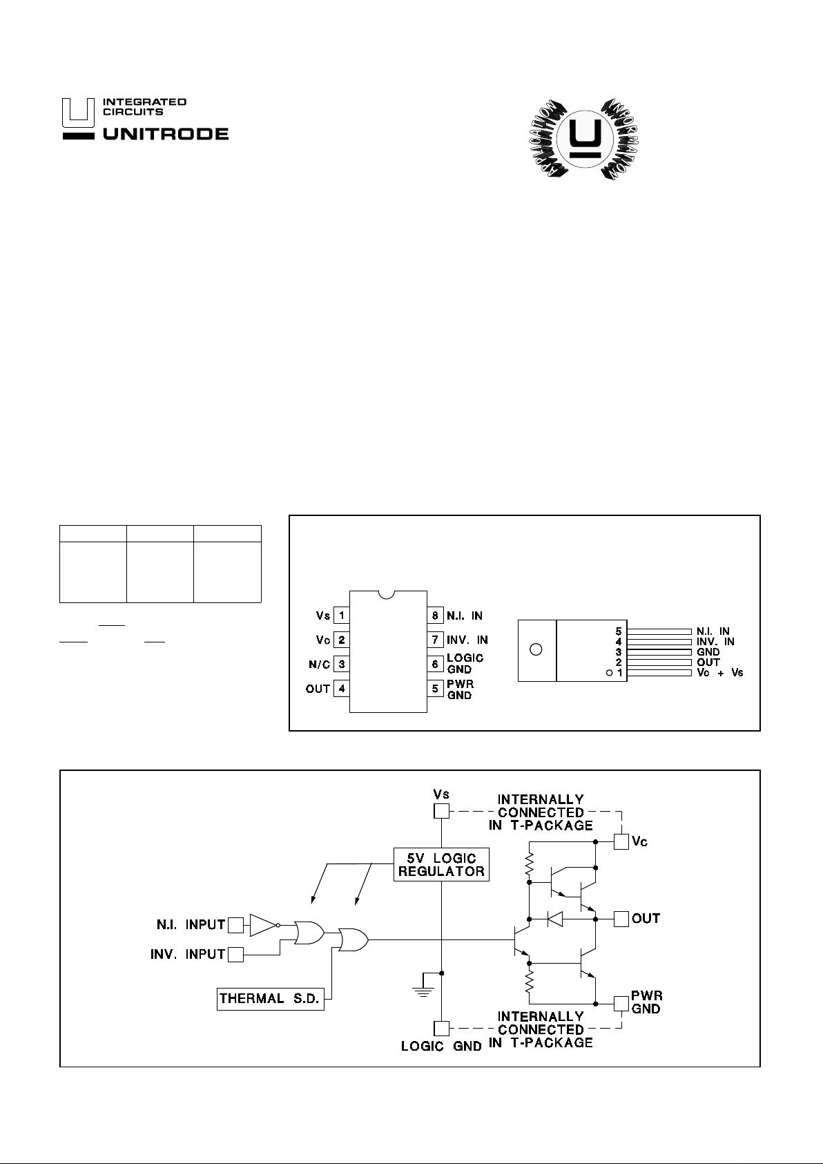
CONNECTION DIAG RAMS
BLOCK DIAGRAM
DESCRIPTI ON
The UC1705 family of p ower drivers is made with a high speed Schottky process to interface between low-level control functions and high-power switching
devices - particularly power MOSFETs. These devices are also an optimum
choice for capacitive line drivers where up to 1.5 amps may be switched in
either direction. With both Inverting and Non-Inverting inputs available, logic
signals o f either polarity may be accepted, or one input can be used to gate or
strobe the other.
Supply voltages for both V
S and VC can independ ently range from 5V to 40V.
For additional application details, see the UC1707/3707 data sheet.
The UC1705 is packaged i n an 8-pin hermetically sealed CERDIP for -55°C to
+125°C operation. The UC3705 i s spe cified for a temperature rang e of 0°C to
+70°C and is available in either a plastic minidip or a 5-pin, power TO-220
package.
DIL-8 MINIDIP, SOIC-8
(TOP VIEW)
N or J Package, D Package
5-PIN TO-220
(TOP VIEW)
T Package
1/94
Page 2
ABSOLUTE MAXI MUM RATING S
N-Pkg J-Pkg T-Pkg
Supply Voltage, V
IN . . . . . . . . . . . . . . . . . . . . . . . . . . . . . . . . 40V. . . . . . . . . . . . . . . . . . . 40V . . . . . . . . . . . . . . . . . . . 40V
Collector Supply Voltage, V
C . . . . . . . . . . . . . . . . . . . . . . . . . 40V. . . . . . . . . . . . . . . . . . . 40V . . . . . . . . . . . . . . . . . . . 40V
Output Current (Source or Sink)
Steady-St ate . . . . . . . . . . . . . . . . . . . . . . . . . . . . . . . . . ±500mA. . . . . . . . . . . . . . . . ±500mA. . . . . . . . . . . . . . . . . ±1.0A
Peak Transient. . . . . . . . . . . . . . . . . . . . . . . . . . . . . . . . . . ±1.5A. . . . . . . . . . . . . . . . . . ±1.0A. . . . . . . . . . . . . . . . . . ±2.0A
Capacitiv e D ischar ge Energy . . . . . . . . . . . . . . . . . . . . . . 20 µ J . . . . . . . . . . . . . . . . . . 15µJ . . . . . . . . . . . . . . . . . . 50µJ
Digital Inputs (See Note) . . . . . . . . . . . . . . . . . . . . . . . . . . . . 5.5V . . . . . . . . . . . . . . . . . . 5.5V . . . . . . . . . . . . . . . . . . 5.5V
Power Dissipation at T
A = 25°C (See Note). . . . . . . . . . . . . . . 1W. . . . . . . . . . . . . . . . . . . . 1W. . . . . . . . . . . . . . . . . . . . 3W
Power Dissipation at T
A (Leads/Case) = 25°C (See Note ) . . . 3W. . . . . . . . . . . . . . . . . . . . 2W. . . . . . . . . . . . . . . . . . . 25W
Operating Temper at ure Range . . . . . . . . . . . . . . . . . . . . 0°C to +70°C. . . . . . . . . . -55°C to +125°C . . . . . . . . . . 0°C to +70°C
Storage Temper at ure Ra nge . . . . . . . . . . . . . . . . . . . . -65°C to +150°C . . . . . . . . -65°C to +150°C . . . . . . . . . -65°C to +150°C
Lead Temp erature (Soldering, 1 0 seconds). . . . . . . . . . . . . 300°C. . . . . . . . . . . . . . . . . . 300°C . . . . . . . . . . . . . . . . . 300°C
Note: All currents are pos itive int o, nega tive out of the sp ecif ied te rminal.
Digital Drive can exceed 5. 5V if input cur rent is limited to 10m A
Consult Packag in g Sect ion of Dat aboo k for ther ma l limitations an d cons id era tion s of packa ge.
UC1705
UC2705
UC3705
TYPICAL SWITCHI NG CHARACTERI ST ICS :
PARAMETERS TEST CONDITION S OUTPUT CL = UNIT
From Inv. Input to Output: open 1.0 2.2 nF
Rise Time Delay 60 60 60 ns
10% to 90% Rise 20 40 60 ns
Fall Time Delay 60 60 60 ns
90% to 10% Fall 25 40 50 ns
From N. I. Input to Output:
Rise Time Delay 90 90 90 ns
10% to 90% Rise 20 40 60 ns
Fall Time Delay 60 60 60 ns
90% to 10% Fall 25 40 50 ns
V
C Cross-Conduction
Current Spike Duration
Ouput Rise 25 ns
Output Fall 0 ns
PARAMETERS TEST CONDITION S MIN TYP MAX UNITS
V
S Supply Current VS = 40V, (Outputs High, T Pkg) 6 8 mA
V
S = 40V, (Outputs Low, T Pkg) 8 12 mA
V
C Supply Current (N, J O nly) VC = 40V, Outputs Low 2 4 mA
V
C Leakage Current (N, J On ly ) VS = 0, V C = 30V .05 0.1 mA
Digital Input Low Level 0.8 V
Digital Input High Level 2.2 V
Input Current V
I = 0 -0.6 -1.0 mA
Input Leakage V
I = 5V 0.5 0.1 mA
Output High Sat., V
C-VO IO = -50mA 2.0 V
I
O = -500mA 2.5 V
Output Low Sat., V
O IO = 50mA 0.4 V
I
O = 500mA 2.5 V
Thermal Shutdown 155 °C
V
S = VC = 20V, TA
= 25°C. Delays measured to 10% output chan ge.
Unless otherwise stated , thes e specificat ions apply for T
A = -55°C to +125°C for the
UC1705, -25°C to +85°C for the UC2705, and 0°C to +70°C for the UC3705; V
S = VC
= 20V, TA = TJ.
ELECTRICAL CHARACTERISTICS:
2
Page 3

UC1705
UC2705
UC3705
APPLICATIONS
UNITRODE INTEGRATED CIRCUITS
7 CONTINENTAL BLVD. •• MERRIMACK NH 03054
TEL. (603 424-2410 • FAX (603) 424-3460
D1, D2: UC3611 Schottky Diodes
D1, D2: UC3611 Schottky Diodes
D1, D2: UC361 1 Schottky Diodes
Transformer Coupled MOSFET Drive Circuit Charge Pump Circuits
Power MO SFET Drive Circuit
Power MOSFET Drive Circu it usi ng Negat ive Bias Voltage and Level
Shifti ng to Ground Referenced PWMs.
3
Page 4

IMPORTANT NOTICE
T exas Instruments and its subsidiaries (TI) reserve the right to make changes to their products or to discontinue
any product or service without notice, and advise customers to obtain the latest version of relevant information
to verify, before placing orders, that information being relied on is current and complete. All products are sold
subject to the terms and conditions of sale supplied at the time of order acknowledgement, including those
pertaining to warranty, patent infringement, and limitation of liability.
TI warrants performance of its semiconductor products to the specifications applicable at the time of sale in
accordance with TI’s standard warranty. Testing and other quality control techniques are utilized to the extent
TI deems necessary to support this warranty. Specific testing of all parameters of each device is not necessarily
performed, except those mandated by government requirements.
CERT AIN APPLICATIONS USING SEMICONDUCTOR PRODUCTS MAY INVOLVE POTENTIAL RISKS OF
DEATH, PERSONAL INJURY, OR SEVERE PROPERTY OR ENVIRONMENTAL DAMAGE (“CRITICAL
APPLICATIONS”). TI SEMICONDUCTOR PRODUCTS ARE NOT DESIGNED, AUTHORIZED, OR
WARRANTED TO BE SUITABLE FOR USE IN LIFE-SUPPORT DEVICES OR SYSTEMS OR OTHER
CRITICAL APPLICATIONS. INCLUSION OF TI PRODUCTS IN SUCH APPLICA TIONS IS UNDERSTOOD T O
BE FULLY AT THE CUSTOMER’S RISK.
In order to minimize risks associated with the customer’s applications, adequate design and operating
safeguards must be provided by the customer to minimize inherent or procedural hazards.
TI assumes no liability for applications assistance or customer product design. TI does not warrant or represent
that any license, either express or implied, is granted under any patent right, copyright, mask work right, or other
intellectual property right of TI covering or relating to any combination, machine, or process in which such
semiconductor products or services might be or are used. TI’s publication of information regarding any third
party’s products or services does not constitute TI’s approval, warranty or endorsement thereof.
Copyright 1999, Texas Instruments Incorporated
 Loading...