

Page 1
250 MHz Demodulating
a
FEATURES
Logarithmic Amplifier Performance
Usable to 250 MHz
44 dB Dynamic Range
ⴞ2.0 dB Log Conformance
37.5 mV/dB Voltage Output
Stable Slope and Intercepts
2.0 nV/√Hz Input Noise Voltage
50 V Input Offset Voltage
Low Power
ⴞ5 V Supply Operation
9 mA (+V
Onboard Resistors
Onboard 10ⴛ Attenuator
Dual Polarity Current Outputs
Direct Coupled Differential Signal Path
APPLICATIONS
IF/RF Signal Processing
Received Signal Strength Indicator (RSSI)
High Speed Signal Compression
High Speed Spectrum Analyzer
ECM/Radar
PRODUCT DESCRIPTION
The AD641 is a 250 MHz, demodulating logarithmic amplifier
with an accuracy of ±2.0 dB and 44 dB dynamic range. The
AD641 uses a successive detection architecture to provide an
output current that is logarithmically proportional to its input
voltage. The output current can be converted to a voltage using
one of several on-chip resistors to select the slope. A single
AD641 provides up to 44 dB of dynamic range at speeds up to
250 MHz, and two cascaded AD641s together can provide
58 dB of dynamic range at speeds up to 250 MHz. The AD641
is fully stable and well characterized over either the industrial or
military temperature ranges.
The AD641 is not a logarithmic building block, but rather a
complete logarithmic solution for compressing and measuring
wide dynamic range signals. The AD641 is comprised of five
stages and each stage has a full wave rectifier, whose current
depends on the absolute value of its input voltage. The output
of these stages are summed together to provide the demodulated
output current scaled at 1 mA per decade (50 µA/dB).
Without utilizing the 10× input attenuator, log conformance of
2.0 dB is maintained over the input range –44 dBm to 0 dBm.
The attenuator offers the most flexibility without significantly
impacting performance.
), 35 mA (–VS) Quiescent Current
S
Logarithmic Amplifier
AD641
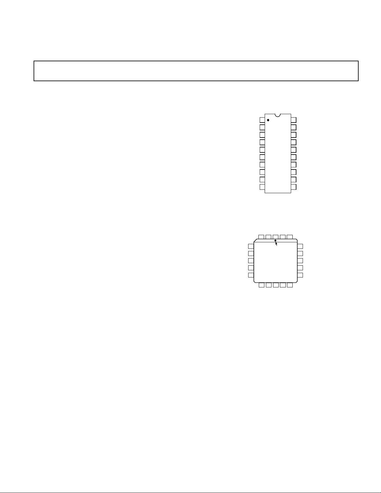
PIN CONFIGURATIONS
20-Lead Plastic DIP (N)
20-Lead Cerdip (Q)
–INPUT
+INPUT
PIN 1
IDENTIFIER
S
+V
SIG +OUT
20
+INPUT
19
ATN OUT
18
17
RG1
16
RG0
15
RG2
14
LOG OUT
13
LOG COM
12
+V
S
11
+OUTPUT
ATN OUT
18
17
16
15
14
LOG COM
CKT COM
RG1
RG0
RG2
LOG OUT
1
–INPUT
2
ATN LO
ATN IN
BL1
–V
ITC
BL2
3
4
5
6
7
S
8
9
10
AD641
TOP VIEW
(Not to Scale)
ATN COM CKT COM
ATN COM
–OUTPUT
20-Lead PLCC (P)
ATN COM
ATN LO
3 2 1 20 19
ATN IN
BL1
–V
ITC
4
5
6
7
S
8
AD641
TOP VIEW
(Not to Scale)
9 10 11 12 13
BL2
SIG –OUT
ATN COM
The 250 MHz bandwidth and temperature stability make this
product ideal for high speed signal power measurement in RF/
IF systems. ECM/Radar and Communication applications are
routinely in the 100 MHz–180 MHz range for power measurement. The bandwidth and accuracy, as well as dynamic range,
make this part ideal for high speed, wide dynamic range signals.
The AD641 is offered in industrial (–40°C to +85°C) and military (–55°C to +125°C) package temperature ranges. Industrial
versions are available in plastic DIP and PLCC; MIL versions
are packaged in cerdip.
REV. C
Information furnished by Analog Devices is believed to be accurate and
reliable. However, no responsibility is assumed by Analog Devices for its
use, nor for any infringements of patents or other rights of third parties
which may result from its use. No license is granted by implication or
otherwise under any patent or patent rights of Analog Devices.
One Technology Way, P.O. Box 9106, Norwood, MA 02062-9106, U.S.A.
Tel: 781/329-4700 World Wide Web Site: http://www.analog.com
Fax: 781/326-8703 © Analog Devices, Inc., 1999
Page 2

AD641–SPECIFICATIONS
ELECTRICAL CHARACTERISTICS
(VS = ⴞ5 V; TA = +25ⴗC, unless otherwise noted)
AD641A AD641S
Parameter Conditions Min Typ Max Min Typ Max Units
TRANSFER FUNCTION
1
(I
= IY LOG |VIN/VX|for V
OUT
= 0.75 mV to ±200 mV dc)
IN
LOG AMPLIFIER PERFORMANCE
3 dB Bandwidth 250 250 MHz
Voltage Compliance Range –0.3 +V
Slope Current, I
Y
0.98 1.00 1.02 0.98 1.00 1.02 mA
– 1 –0.3 +VS – 1 V
S
Accuracy vs. Temperature 0.002 0.002 %/°C
Over Temperature T
MIN
to T
MAX
0.98 1.02 mA
Intercept dBm 250 MHz –40.84 –40.43 –39.96 –40.84 –40.43 –39.96 dBm
Over Temperature T
Zero Signal Output Current
2
MIN
to T
250 MHz –40.59 –39.47 dBm
MAX,
–0.2 –0.2 mA
ITC Disabled Pin 8 to COM –0.27 –0.27 mA
Maximum Output Current 2.3 2.3 mA
DYNAMIC RANGE
Single Configuration 44 44 dB
Over Temperature T
MIN
to T
MAX
40 38 dB
Dual Configuration 58 58 dB
Over Temperature T
MIN
to T
MAX
52 52 dB
LOG CONFORMANCE f = 250 MHz
Single Configuration –44 dBm to 0 dBm ±0.5 ±2.0 ±0.5 ±2.0 dB
Over Temperature –42 dBm to –4 dBm; T
–42 dBm to –2 dBm, T
MIN
MIN
to T
to T
MAX
MAX
±1.0 ±2.5
±1.0 ±2.5 dB
Dual Configuration S: –60 dBm to –2 dBm; ±0.5 ±2.0 ±0.5 ±2.0 dB
Over Temperature A: –56 dBm to –4 dBm, T
MIN
to T
MAX
±1.0 ±2.5 ±1.0 ±2.5 dB
LIMITER CHARACTERISTICS
Flatness –44 dBm to 0 dBm @ 10.7 MHz ±1.6 ±1.6 dB
Phase Variation –44 dBm to 0 dBm @ 10.7 MHz ±2.0 ±2.0 Degrees
INPUT CHARACTERISTICS
Input Resistance Differential 500 500 kΩ
Input Offset Voltage Differential 50 200 50 200 µV
vs. Temperature 0.8 0.8 µV/°C
Over Temperature T
MIN
to T
MAX
300 µV
vs. Supply 22µV/V
Input Bias Current 7 25 7 25 µA
Input Bias Offset 11µA
Common Mode Input Range –2 +0.3 –2 +0.3 V
SIGNAL INPUT (Pins 1, 20)
Input Capacitance Either Pin to COM 2 2 pF
Noise Spectral Density 1 kHz to 10 MHz 2 2 nV/√Hz
Tangential Sensitivity BW = 100 MHz –72 –72 dBm
INPUT ATTENUATOR
(Pins 2, 3, 4, 5 & 19)
Attenuation
3
Pins 5 to Pin 19 20 20 dB
Input Resistance Pins 5 to 3/4 300 300 Ω
APPLICATION RESISTORS
(Pins 15, 16, 17) 0.995 1.000 1.005 0.995 1.000 1.005 kΩ
OUTPUT CHARACTERISTICS
(Pins 10, 11)
Peak Differential Output
4
±180 ±180 mV
Output Resistance Either Pin to COM 75 75 Ω
Quiescent Output Voltage Either Pin to COM –90 –90 mV
POWER SUPPLY
Voltage Supply Range ±4.5 ±7.5 ±4.5 ±7.5 V
Quiescent Current
(Pin 12) T
+V
S
–VS (Pin 7) T
NOTES
1
Logarithms to base 10 are used throughout. The response is independent of the sign of VIN.
2
The zero-signal current is a function of temperature unless internal temperature compensation (ITC) pin is grounded.
3
Attenuation ratio trimmed to calibrate intercept to 10 mV when in use. It has a temperature coefficient of +0.3%/°C.
4
The fully limited signal output will appear to be a square wave; its amplitude is proportional to absolute temperature.
Specifications subject to change wi
thout notice.
MIN
MIN
to T
to T
MAX
MAX
915 9 15 mA
35 60 35 60 mA
–2–
REV. C
Page 3
AD641
WARNING!
ESD SENSITIVE DEVICE
ORDERING GUIDE
Temperature Package Package
Model Range Description Option
AD641AN –40°C to +85°C Plastic DIP N-20
AD641AP –40°C to +85°C PLCC P-20A
5962-9559801MRA –55°C to +125°C Cerdip Q-20
AD641-EB Evaluation Board
ABSOLUTE MAXIMUM RATINGS*
Supply Voltages . . . . . . . . . . . . . . . . . . . . . . . . . . . . . . . ±7.5 V
Input Voltage (Pin 1 or Pin 20 to COM) . . . –3 V to +300 mV
Attenuator Input Voltage (Pin 5 to Pin 3/4) . . . . . . . . . . . ±4 V
Storage Temperature Range, Q . . . . . . . . . . –65°C to +150°C
Storage Temperature Range, N, P . . . . . . . . –65°C to +125°C
Ambient Temperature Range, Rated Performance
Industrial, AD641A . . . . . . . . . . . . . . . . . . –40°C to +85°C
Military, AD641S . . . . . . . . . . . . . . . . . . –55°C to +125°C
THERMAL CHARACTERISTICS
JC
(ⴗC/W) (ⴗC/W)
20-Lead Plastic DIP Package (N) 24 61
JA
Lead Temperature Range (Soldering 60 sec) . . . . . . . . +300°C
*Stresses above those listed under Absolute Maximum Ratings may cause perma-
nent damage to the device. This is a stress rating only; functional operation of the
device at these or any other conditions above those indicated in the operational
section of this specification is not implied. Exposure to absolute maximum rating
conditions for extended periods may adversely affect device reliability.
20-Lead Cerdip Package (Q) 25 85
20-Lead Plastic Leadless Chip Carrier (P) 28 75
CAUTION
ESD (electrostatic discharge) sensitive device. Electrostatic charges as high as 4000 V readily
accumulate on the human body and test equipment and can discharge without detection.
Although the AD641 features proprietary ESD protection circuitry, permanent damage may
occur on devices subjected to high energy electrostatic discharges. Therefore, proper ESD
precautions are recommended to avoid performance degradation or loss of functionality.
REV. C
–3–
Page 4
AD641
(
)
4.5 5.0 5.5 6.0 6.5 7.0 7.5
POWER SUPPLY VOLTAGES – 6 Volts
SLOPE CURRENT – mV
1.006
1.004
1.002
1.000
0.998
0.996
0.994
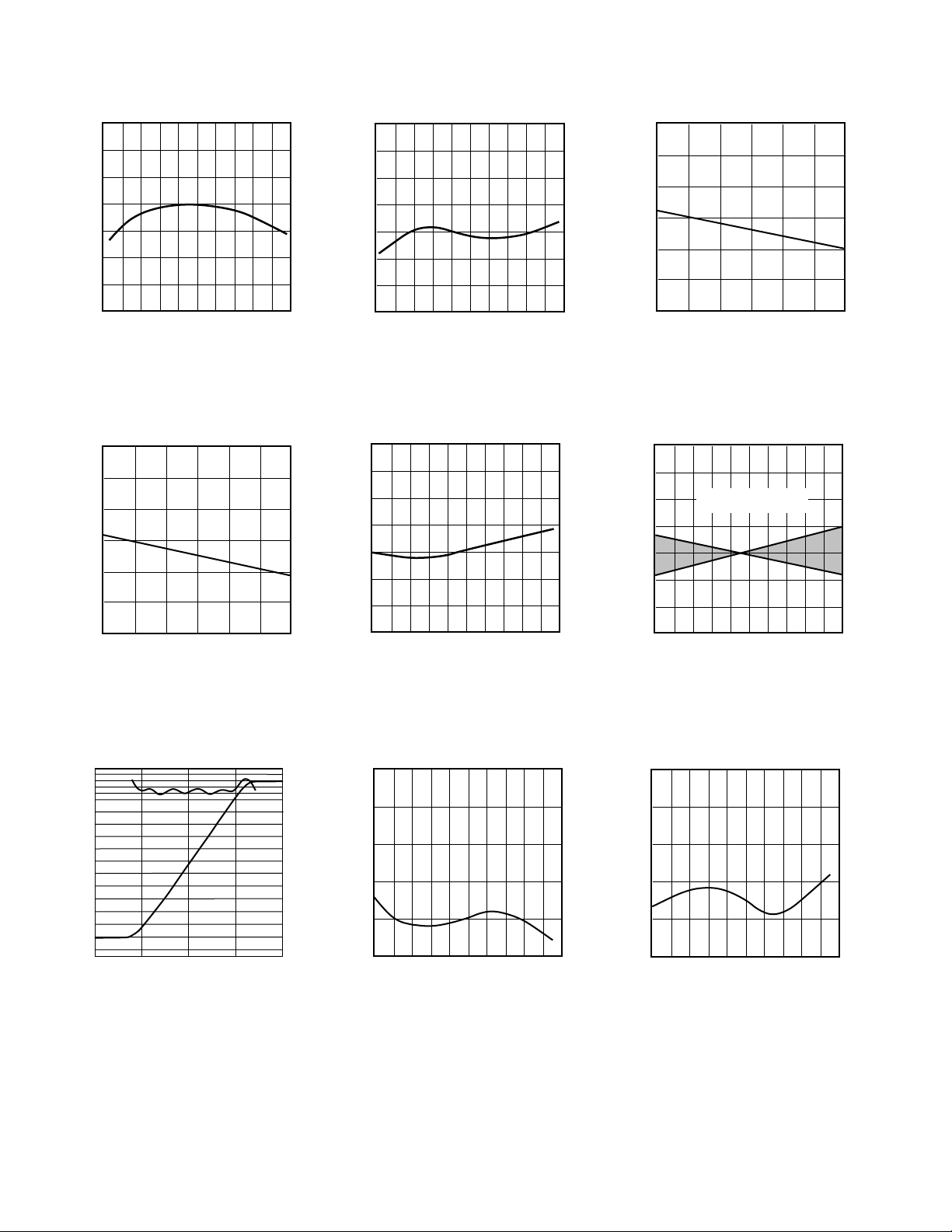
–Typical DC Performance Characteristics
1.015
1.010
1.005
1
0.995
0.990
SLOPE CURRENT – mA
0.985
0.980
–60 –40 –20 0 20 40 60 80 100 120 140
TEMPERATURE – 8C
Figure 1. Slope Current, IY, vs.
Temperature
1.015
1.010
1.005
1.000
0.995
0.990
INTERCEPT VOLTAGE – mV
0.985
4.5 5.0 5.5 6.0 6.5 7.0 7.5
POWER SUPPLY VOLTAGES – 6 Volts
Figure 4. Intercept Voltage, VX, vs.
Supply Voltages
1.20
1.15
1.10
1.05
1.00
INTERCEPT – mV
0.95
0.90
0.85
–60 –40 –20 0 20 40 60 80 100 120 140
TEMPERATURE – 8C
Figure 2. Intercept Voltage, VX, vs.
Temperature
14
13
12
11
10
INTERCEPT – mV
9
8
7
–60 –40 –20 0 20 40 60 80 100 120 140
TEMPERATURE – 8C
Figure 5. Intercept Voltage (Using
Attenuator) vs. Temperature
Figure 3. Slope Current, IY, vs. Supply
Voltages
+0.4
+0.3
+0.2
+0.1
0
–0.1
–0.2
–0.3
–60 –40 –20 0 20 40 60 80 100 120 140
DEVIATION OF INPUT OFFSET VOLTAGE – mV
INPUT OFFSET VOLTAGE
DEVIATION WILL BE WITHIN
SHADED AREA.
TEMPERATURE – 8C
Figure 6. Input Offset Voltage Deviation vs. Temperature
2.4
2.2
2.0
1.8
1.6
1.4
1.2
1.0
0.8
0.6
0.4
0.2
OUTPUT CURRENT – mA
0
–0.2
–0.4
0.1 1.0 1000.010.0 100.0
Figure 7. DC Logarithmic Transfer
Function and Error Curve for Single
AD641
INPUT VOLTAGE – mV
EITHER SIGN
2
1
0
ERROR – dB
2.5
2.0
1.5
1.0
ABSOLUTE ERROR – dB
0.5
0
–60 –40 –20 0 20 40 60 80 100 120 140
TEMPERATURE – 8C
Figure 8. Absolute Error vs. Temperature, V
= ±1 mV to ±100 mV
IN
–4–
2.5
2.0
1.5
1.0
ABSOLUTE ERROR – dB
0.5
0
–60 –40 –20 0 20 40 60 80 100 120 140
TEMPERATURE – 8C
Figure 9. Absolute Error vs. Temperature, Using Attenuator. V
±
1 V, Pin 8 Grounded to Disable ITC
to
= ±10 mV
IN
Bias
REV. C
Page 5
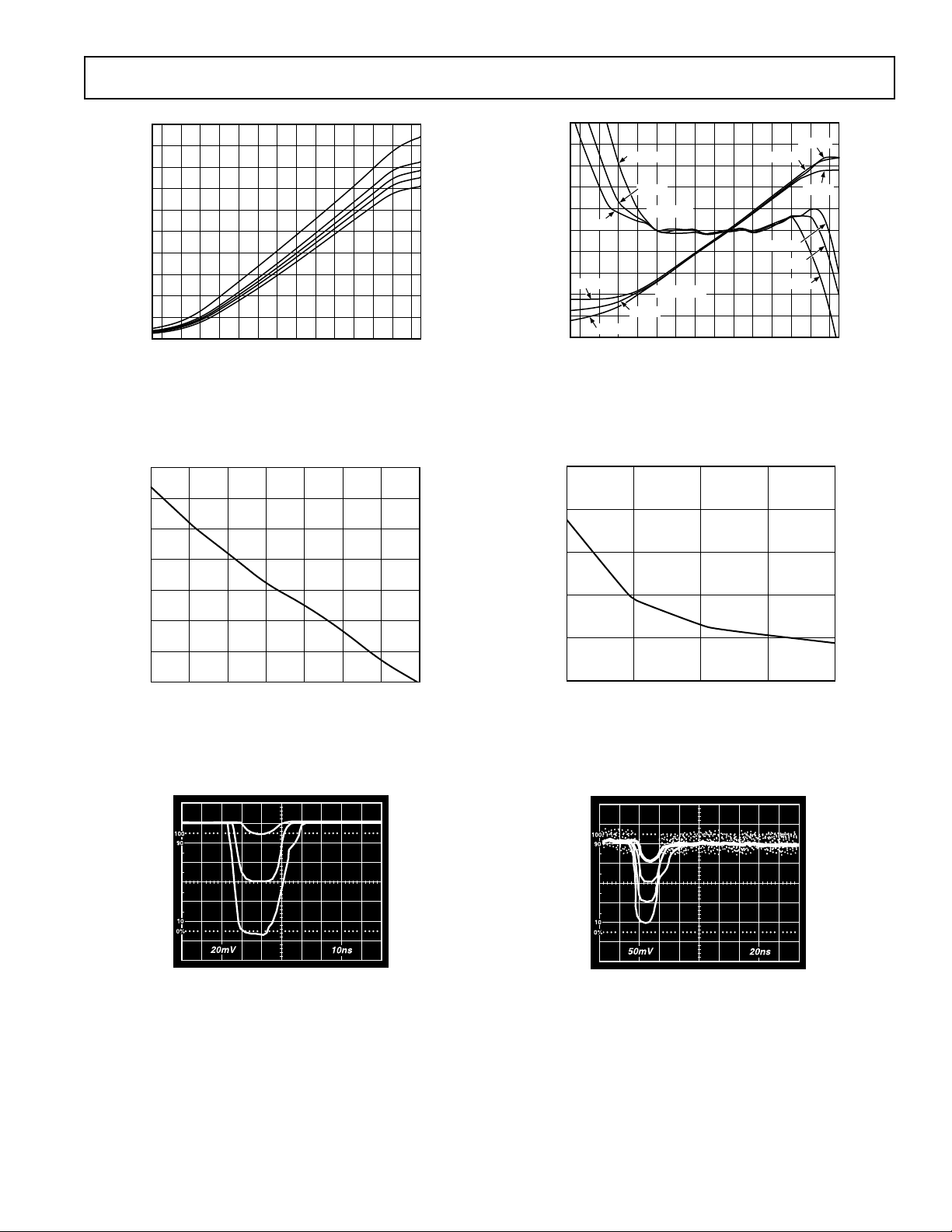
Typical AC Performance Characteristics–
AD641
–2.25
–2.00
–1.75
–1.50
–1.25
–1.00
–0.75
–0.50
OUTPUT CURRENT – mA
–0.25
0.00
0.25
–52 –36 –32 –28 –24 –20 –16 –12 –8 0
–40
INPUT LEVEL – dBm
50MHz
150MHz
190MHz
210MHz
250MHz
2–48 –44
–4
Figure 10. AC Response at 50 MHz, 150 MHz, 190 MHz,
210 MHz at 250 MHz, vs. dBm Input (Sinusoidal Input)
87.5
85.0
82.5
80.0
–2.00
–1.75
–1.50
–1.25
–1.00
–0.75
–0.50
OUTPUT – mA
–0.25
+1258C
–0.00
0.25
0.50
–52 –36 –32 –28 –24 –20 –16 –12 –8 0
–558C
–558C
+1258C
+258C
ERROR
OUTPUT
+258C
–40
INPUT LEVEL – dBm
+258C
+1258C
+258C
–558C
+1258C
–558C
–4
5
4
3
2
1
0
–1
–2
–3
–4
–5
2–48 –44
Figure 13. Logarithmic Response and Linearity at
200 MHz, T
1.0
0.95
0.90
for TA = –55°C, +25°C, +125°C
A
ERROR IN – dB
77.5
75.0
INTERCEPT LEVEL – dBm
72.5
70.0
50 250100 150 170 190 210 230
INPUT FREQUENCY – MHz
Figure 11. Intercept Level (dBm) vs. Frequency (Cascaded
AD641s—Sinusoidal Input)
Figure 12. Baseband Pulse Response of Single AD641,
Inputs of 1 mV, 10 mV and 100 mV
0.85
SLOPE CURRENT – mA
0.80
0.75
50 250150 190 210
INPUT FREQUENCY – MHz
Figure 14. Slope Current, IY, vs. Input Frequency
5µs
100
90
10
0%
20mV
5µs
20mV
Figure 15. Baseband Pulse Response of Cascaded AD641s
at Inputs of 0.2 mV, 2 mV, 20 mV and 200 mV
REV. C
–5–
Page 6

AD641
CIRCUIT DESCRIPTION
The AD641 uses five cascaded limiting amplifiers to approximate a logarithmic response to an input signal of wide dynamic
range and wide bandwidth. This type of logarithmic amplifier
has traditionally been assembled from several small scale ICs
and numerous external components. The performance of these
semidiscrete circuits is often unsatisfactory. In particular, the
logarithmic slope and intercept (see FUNDAMENTALS OF
LOGARITHMIC CONVERSION) are usually not very stable
in the presence of supply and temperature variations even after
laborious and expensive individual calibration. The AD641 employs high precision analog circuit techniques to ensure stability
of scaling over wide variations in supply voltage and temperature. Laser trimming, using ac stimuli and operating conditions
similar to those encountered in practice, provides fully calibrated logarithmic conversion.
Each of the amplifier/limiter stages in the AD641 has a small
signal voltage gain of 10 dB (×3.162) and a –3 dB bandwidth of
350 MHz. Fully differential direct coupling is used throughout.
This eliminates the many interstage coupling capacitors usually
required in ac applications, and simplifies low frequency signal
processing, for example, in audio and sonar systems. The AD641
is intended for use in demodulating applications. Each stage
incorporates a detector (a full-wave transconductance rectifier)
whose output current depends on the absolute value of its input
voltage.
Figure 16 is a simplified schematic of one stage of the AD641.
All transistors in the basic cell operate at near zero collector to
base voltage and low bias currents, resulting in low levels of
thermally induced distortion. These arise when power shifts
from one set of transistors to another during large input signals.
Rapid recovery is essential when a small signal immediately
follows a large one. This low power operation also contributes
significantly to the excellent long term calibration stability of the
AD641.
The complete AD641, shown in Figure 17, includes two bias
regulators. One determines the small signal gain of the amplifier stages; the other determines the logarithmic slope. These
bias regulators maintain a high degree of stability in the resulting function by compensating for potentially large uncertainties in transistor parameters, temperature and supply
voltages. A third biasing block is used to accurately control
the logarithmic intercept.
COM
RG1 RG0 RG2
18
1kV 1kV
151617
LOG OUT
LOG COM
14
LOG OUT LOG COM
COMMON
SIG
IN
1.09mA
PTAT
Q1
R1
85V
Q2
1.09mA
PTAT
R2
85V
Q9
Q3
565mA
Q4
Q5 Q6
565mA
Q10
75V
R3
Q7
2.18mA
PTAT
Q8
R4
75V
SIG
OUT
–V
S
Figure 16. Simplified Schematic of a Single AD641 Stage
By summing the signals at the output of the detectors, a good
approximation to a logarithmic transfer function can be achieved.
The lower the stage gain, the more accurate the approximation,
but more stages are then needed to cover a given dynamic range.
The choice of 10 dB results in a theoretical periodic deviation or
ripple in the transfer function of ±0.15 dB from the ideal re-
sponse when the input is either a dc voltage or a square wave.
The slope of the transfer function is unaffected by the input
waveform; however, the intercept and ripple are waveform dependent (see EFFECT OF WAVEFORM ON INTERCEPT).
The input will usually be an amplitude modulated sinusoidal
carrier. In these circumstances the output is a fluctuating current at twice the carrier frequency (because of the full wave
detection) whose average value is extracted by an external low
pass filter, which recovers a logarithmic measure of the baseband signal.
Circuit Operation
With reference to Figure 16, the transconductance pair Q7, Q8
and load resistors R3 and R4 form a limiting amplifier having a
small signal gain of 10 dB, set by the tail current of nominally
2.18 mA at 27°C. This current is basically proportional to abso-
lute temperature (PTAT) but includes additional current to
compensate for finite beta and junction resistance. The limiting
output voltage is ±180 mV at +27°C and is PTAT. Emitter
followers Q1 and Q2 raise the input resistance of the stage,
provide level shifting to introduce collector bias for the gain
stage and detectors, reduce offset drift by forming a thermally
balanced quad with Q7 and Q8 and generate the detector biasing across resistors R1 and R2.
13
INTERCEPT POSITIONING BIAS
+V
12
S
ATN OUT
SIG +IN
SIG –IN
ATN LO
ATN COM
ATN COM
FULL-WAVE
19
20
1
2
27V
3
30V
4
DETECTOR
10dB
AMPLIFIER/LIMITER
270V
5
ATN IN
6
BL1
FULL-WAVE
DETECTOR
10dB
AMPLIFIER/LIMITER
GAIN BIAS REGULATOR
FULL-WAVE
DETECTOR
10dB
AMPLIFIER/LIMITER
7
–V
S
FULL-WAVE
DETECTOR
10dB
AMPLIFIER/LIMITER
SLOPE BIAS REGULATOR
FULL-WAVE
DETECTOR
10dB
AMPLIFIER/LIMITER
11
10
9
8
SIG +OUT
SIG –OUT
BL2
ITC
Figure 17. Block Diagram of the Complete AD641
–6–
REV. C
Page 7

AD641
Transistors Q3 through Q6 form the full wave detector, whose
output is buffered by the cascodes Q9 and Q10. For zero input
Q3 and Q5 conduct only a small amount (a total of about 32 µA)
of the 565 µA tail currents supplied to pairs Q3–Q4 and Q5–Q6.
This “pedestal” current flows in output cascode Q9 to the LOG
OUT node (Pin 14). When driven to the peak output of the
preceding stage, Q3 or Q5 (depending on signal polarity) con-
ducts most of the tail current, and the output rises to 532 µA.
The LOG OUT current has thus changed by 500 µA as the
input has changed from zero to its maximum value. Since the
detectors are spaced at 10 dB intervals, the output increases by
50 µA/dB, or 1 mA per decade. This scaling parameter is trimmed
to absolute accuracy using a 2 kHz square wave. At frequencies
near the system bandwidth, the slope is reduced due to the
reduced output of the limiter stages, but it is still relatively insensitive to temperature variations so that a simple external
slope adjustment can restore scaling accuracy.
The intercept position bias generator (Figure 17) removes the
pedestal current from the summed detector outputs. It is adjusted during manufacture such that the output (flowing into
Pin 14) is 1 mA when a 2 kHz square-wave input of exactly
±10 mV is applied to the AD641. This places the dc intercept at
precisely 1 mV. The LOG COM output (Pin 13) is the complement of LOG OUT. It also has a 1 mV intercept, but with an
inverted slope of –1 mA/decade. Because its pedestal is very
large (equivalent to about 100 dB), its intercept voltage is not
guaranteed. The intercept positioning currents include a special
internal temperature compensation (ITC) term which can be
disabled by connecting Pin 8 to ground.
The logarithmic function of the AD641 is absolutely calibrated
to within ±0.3 dB (or ±15 µA) for 2 kHz square-wave inputs of
±1 mV to ±100 mV, and to within ±1 dB between ±750 µV and
±200 mV. Figure 18 is a typical plot of the dc transfer function,
2.5
2.0
1.5
1.0
0.5
OUTPUT CURRENT – mA
0
–0.5
1.00.1
INPUT VOLTAGE – mV
–558C
+258C
100.010.0
+1258C
+1258C
+258C
–558C
3
2
1
0
–1
–2
ABSOLUTE ERROR – dB
1000.0
Figure 18. Logarithmic Output and Absolute Error vs. DC
or Square Wave Input at T
= –55°C, +25°C, and +125°C,
A
Input Direct to Pins 1 and 20
2.5
–558C
2.0
1.5
1.0
0.5
OUTPUT CURRENT – mA
0
–0.5
+858C
100.1
+258C
+1258C
INPUT VOLTAGE – mV
1000100
1
0
–1
–2
ABSOLUTE ERROR – dB
10000
Figure 19. Logarithmic Output and Absolute Error vs. DC
or Square Wave Input at T
°
C. Input via On-Chip Attenuator
+125
= –55°C, +25°C, +85°C and
A
showing the outputs at temperatures of –55°C, +25°C and
+125°C. While the slope and intercept are seen to be little af-
fected by temperature, there is a lateral shift in the end points of
the “linear” region of the transfer function, which reduces the
effective dynamic range.
The on chip attenuator can be used to handle input levels 20 dB
higher, that is, from ±7.5 mV to ±2 V for dc or square wave
inputs. It is specially designed to have a positive temperature
coefficient and is trimmed to position the intercept at 10 mV dc
(or –24 dBm for a sinusoidal input) over the full temperature
range. When using the attenuator the internal bias compensation should be disabled by grounding Pin 8. Figure 19 shows
the output at –55°C, +25°C, +85°C and +125°C for a single,
AD641 with the attenuator in use; the curves overlap almost
perfectly, and the lateral shift in the transfer function does not
occur. Therefore, the full dynamic range is available at all
temperatures.
The output of the final limiter is available in differential form at
Pins 10 and 11. The output impedance is 75 Ω to ground from
either pin. For most input levels, this output will appear to have
roughly a square waveform. The signal path may be extended
using these outputs (see OPERATION OF CASCADED
AD641s). The logarithmic outputs from two or more AD641s
can be directly summed with full accuracy.
A pair of 1 kΩ applications resistors, RG1 and RG2 (Figure 17)
are accessed via Pins 15, 16 and 17. These can be used to convert an output current to a voltage, with a slope of 1 V/decade
(using one resistor), 2 V/decade (both resistors in series) or
0.5 V/decade (both in parallel). Using all the resistors from two
AD641s (for example, in a cascaded configuration) ten slope
options from 0.25 V to 4 V/decade are available.
REV. C
–7–
Page 8

AD641
FUNDAMENTALS OF LOGARITHMIC CONVERSION
The conversion of a signal to its equivalent logarithmic value
involves a nonlinear operation, the consequences of which can be
very confusing if not fully understood. It is important to realize
from the outset that many of the familiar concepts of linear
circuits are of little relevance in this context. For example, the
incremental gain of an ideal logarithmic converter approaches
infinity as the input approaches zero. Further, an offset at the
output of a linear amplifier is simply equivalent to an offset at
the input, while in a logarithmic converter it is equivalent to a
change of amplitude at the input—a very different relationship.
We assume a dc signal in the following discussion to simplify the
concepts; ac behavior and the effect of input waveform on calibration are discussed later. A logarithmic converter having a
voltage input V
and output V
IN
must satisfy a transfer func-
OUT
tion of the form
V
= VY LOG (VIN/VX) Equation (1)
OUT
where V
and VX are fixed voltages which determine the scaling
Y
of the converter. The input is divided by a voltage because the
argument of a logarithm has to be a simple ratio. The logarithm
must be multiplied by a voltage to develop a voltage output.
These operations are not, of course, carried out by explicit computational elements, but are inherent in the behavior of the
converter. For stable operation, V
and VY must be based on
X
sound design criteria and rendered stable over wide temperature
and supply voltage extremes. This aspect of RF logarithmic
amplifier design has traditionally received little attention.
When V
the Intercept Voltage, because a graph of V
(V
IN
point (see Figure 20). For the AD641, V
actly 1 mV. The slope of the line is directly proportional to V
= VX, the logarithm is zero. VX is, therefore, called
IN
versus LOG
OUT
)—ideally a straight line—crosses the horizontal axis at this
is calibrated to ex-
X
.
Y
Base 10 logarithms are used in this context to simplify the relationship to decibel values. For V
value of 1, so the output voltage is V
output is 2 V
, and so on. VY can therefore be viewed either as
Y
= 10 VX, the logarithm has a
IN
At V
Y.
= 100 VX, the
IN
the Slope Voltage or as the Volts per Decade Factor.
The AD641 conforms to Equation (1) except that its two outputs are in the form of currents, rather than voltages:
= IY LOG (VIN/VX) Equation (2)
I
OUT
2V
Y
Y
Y
+
0
–
VYLOG (VIN/VX)
ACTUAL
VIN = V
IDEAL
SLOPE = V
X
Y
VIN = 10V
X
VIN = 100V
IDEAL
ACTUAL
INPUT ON
X
LOG SCALE
Figure 20. Basic DC Transfer Function of the AD641
IY, the Slope Current, is 1 mA. The current output can readily
be converted to a voltage with a slope of 1 V/decade, for ex-
ample, using one of the 1 kΩ resistors provided for this purpose,
in conjunction with an op amp, as shown in Figure 21.
15
AD641
1mA PER DECADE
48.7V
C1
330pF
LOG
LOG
OUT
COM
–V
ITC
S
R1
+V
BL2
11
SIG
S
+OUT
SIG
–OUT
9128137146
10
R2
AD846
OUTPUT VOLTAGE
1V PER DECADE
FOR R2 = 1kV
100mV PER dB
FOR R2 = 2kV
Figure 21. Using an External Op Amp to Convert the
AD641 Output Current to a Buffered Voltage Output
Intercept Stabilization
Internally, the intercept voltage is a fraction of the thermal voltage kT/q, that is, V
= VXOT/TO, where VXO is the value of V
X
X
at a reference temperature TO. So the uncorrected transfer
function has the form:
I
= IY LOG (VIN TO/VXOT) Equation (3)
OUT
Now, if the amplitude of the signal input V
could somehow be
IN
rendered PTAT, the intercept would be stable with temperature, since the temperature dependence in both the numerator
and denominator of the logarithmic argument would cancel.
This is what is actually achieved by interposing the on-chip
attenuator, which has the necessary temperature dependence to
cause the input to the first stage to vary in proportion to absolute temperature. The end limits of the dynamic range are now
totally independent of temperature. Consequently, this is the preferred method of intercept stabilization for applications where
the input signal is sufficiently large.
When the attenuator is not used, the PTAT variation in V
X
will
result in the intercept being temperature dependent. Near 300K
(+27°C) it will vary by 20 LOG (301/300) dB/°C, about 0.03 dB/
°C. Unless corrected, the whole output function would drift up
or down by this amount with changes in temperature. In the
AD641 a temperature compensating current I
LOG(T/TO) is
Y
added to the output. This effectively maintains a constant intercept V
. This correction is active in the default state (Pin 8
XO
open circuited). When using the attenuator, Pin 8 should be
grounded, which disables the compensation current. The drift
term needs to be compensated only once; when the outputs of
two AD641s are summed, Pin 8 should be grounded on at least
one of the two devices (both if the attenuator is used).
Conversion Range
Practical logarithmic converters have an upper and lower limit
on the input, beyond which errors increase rapidly. The upper
limit occurs when the first stage in the chain is driven into limiting. Above this, no further increase in the output can occur and
the transfer function flattens off. The lower limit arises because
a finite number of stages provide finite gain, and therefore at
low signal levels the system becomes a simple linear amplifier.
–8–
REV. C
Page 9

AD641
4
2
0
–2
–4
–6
–8
–10
–70
INPUT AMPLITUDE IN dB ABOVE 1V, AT 10kHz
–60 –50 –40 –30 –20 –10
–12
DEVIATION FROM EXACT LOGARITHMIC
TRANSFER FUNCTION – dB
SQUARE
WAVE INPUT
SINE WAVE
INPUT
TRIWAVE
INPUT
Note that this lower limit is not determined by the intercept
voltage, V
; it can occur either above or below VX, depending
X
on the design. When using two AD641s in cascade, input offset
voltage and wideband noise are the major limitations to low
level accuracy. Offset can be eliminated in various ways. Noise
can only be reduced by lowering the system bandwidth, using a
filter between the two devices.
EFFECT OF WAVEFORM ON INTERCEPT
The absolute value response of the AD641 allows inputs of
either polarity to be accepted. Thus, the logarithmic output in
response to an amplitude-symmetric square wave is a steady
value. For a sinusoidal input the fluctuating output current will
usually be low-pass filtered to extract the baseband signal. The
unfiltered output is at twice the carrier frequency, simplifying the
design of this filter when the video bandwidth must be maximized. The averaged output depends on waveform in a roughly
analogous way to waveform dependence of rms value. The effect
is to change the apparent intercept voltage. The intercept voltage appears to be doubled for a sinusoidal input, that is, the
averaged output in response to a sine wave of amplitude (not rms
value) of 20 mV would be the same as for a dc or square wave
input of 10 mV. Other waveforms will result in different intercept factors. An amplitude-symmetric-rectangular waveform has
the same intercept as a dc input, while the average of a baseband unipolar pulse can be determined by multiplying the
response to a dc input of the same amplitude by the duty cycle.
It is important to understand that in responding to pulsed RF
signals it is the waveform of the carrier (usually sinusoidal) not
the modulation envelope, that determines the effective intercept
voltage. Table I shows the effective intercept and resulting decibel offset for commonly occurring waveforms. The input waveform does not affect the slope of the transfer function. Figure 22
shows the absolute deviation from the ideal response of cascaded
AD641s for three common waveforms at input levels from
–80 dBV to –10 dBV. The measured sine wave and triwave
responses are 6 dB and 8.7 dB, respectively, below the square
wave response—in agreement with theory.
Table I.
Input Peak Intercept Error (Relative
Waveform or rms Factor to a DC Input)
Square Wave Either 1 0.00 dB
Sine Wave Peak 2 –6.02 dB
Sine Wave rms 1.414 (√2) –3.01 dB
Triwave Peak 2.718 (e) –8.68 dB
Triwave rms 1.569 (e/√3) –3.91 dB
Gaussian Noise rms 1.887 –5.52 dB
2
0
–2
–4
–6
TRANSFER FUNCTION – dB
–8
DEVIATION FROM EXACT LOGARITHMIC
–10
–70 –60 –50 –40 –30 –20 –10–80
INPUT AMPLITUDE IN dB ABOVE 1V, AT 10kHz
SQUARE
WAVE INPUT
SINE WAVE
INPUT
TRIWAVE
INPUT
Figure 22. Deviation from Exact Logarithmic Transfer
Function for Two Cascaded AD641s, Showing Effect of
Waveform on Calibration and Linearity
By contrast, a general time varying signal has a continuum of
values within each cycle of its waveform. The averaged output is
thereby “smoothed” because the periodic deviations away from
the ideal response, as the waveform “sweeps over” the transfer
function, tend to cancel. This smoothing effect is greatest for a
triwave input, as demonstrated in Figure 22.
The accuracy at low signal inputs is also waveform dependent.
The detectors are not perfect absolute value circuits, having a
sharp “corner” near zero; in fact they become parabolic at low
levels and behave as if there were a dead zone. Consequently,
the output tends to be higher than ideal. When there are enough
stages in the system, as when two AD641s are connected in
cascade, most detectors will be adequately loaded due to the
high overall gain, but a single AD641 does not have sufficient
gain to maintain high accuracy for low level sine wave or triwave
inputs. Figure 23 shows the absolute deviation from calibration
for the same three waveforms for a single AD641. For inputs
between –10 dBV and –40 dBV the vertical displacement of the
traces for the various waveforms remains in agreement with the
predicted dependence, but significant calibration errors arise at
low signal levels.
Logarithmic Conformance and Waveform
The waveform also affects the ripple, or periodic deviation from
an ideal logarithmic response. The ripple is greatest for dc or
square wave inputs because every value of the input voltage
maps to a single location on the transfer function and thus traces
out the full nonlinearities in the logarithmic response.
REV. C
Figure 23. Deviation from Exact Logarithmic Transfer
Function for a Single AD641, Compare Low Level
Response with That of Figure 22
–9–
Page 10

AD641
SIGNAL MAGNITUDE
The AD641 is a calibrated device. It is, therefore, important to
be clear in specifying the signal magnitude under all waveform
conditions. For dc or square wave inputs there is, of course, no
ambiguity. Bounded periodic signals, such as sinusoids and
triwaves, can be specified in terms of their simple amplitude
(peak value) or alternatively by their rms value (which is a measure of power when the impedance is specified). It is generally better to define this type of signal in terms of its amplitude because
the AD641 response is a consequence of the input voltage, not
power. However, provided that the appropriate value of intercept for a specific waveform is observed, rms measures may be
used. Random waveforms can only be specified in terms of rms
value because their peak value may be unbounded, as is the case
for Gaussian noise. These must be treated on a case-by-case
basis. The effective intercept given in Table I should be used for
Gaussian noise inputs.
On the other hand, for bounded signals the amplitude can be
expressed either in volts or dBV (decibels relative to 1 V). For
example, a sine wave or triwave of 1 mV amplitude can also be
defined as an input of –60 dBV, one of 100 mV amplitude as
–20 dBV, and so on. RMS value is usually expressed in dBm
(decibels above 1 mW) for a specified impedance level. Through-
Ω
out this data sheet we assume a 50
environment, the customary
impedance level for high speed systems, when referring to signal powers in dBm. Bearing in mind the above discussion of the effect of
waveform on the intercept calibration of the AD641, it will be
apparent that a sine wave at a power of, say, –10 dBm will not
produce the same output as a triwave or square wave of the
same power. Thus, a sine wave at a power level of –10 dBm has
an rms value of 70.7 mV or an amplitude of 100 mV (that is, √2
times as large, the ratio of amplitude to rms value for a sine
wave), while a triwave of the same power has an amplitude
which is √3 or 1.73 times its rms value, or 122.5 mV.
“Intercept” and “Logarithmic Offset”
If the signals are expressed in dBV, we can write the output
current in a simpler form, as:
I
= 50µA (Input
OUT
where Input
and X
is the appropriate value of the intercept (for a given wave-
dBV
is the input voltage amplitude (not rms) in dBV
dBV
dBV
– X
) Equation (4)
dBV
form) in dBV. This form shows more clearly why the intercept is
often referred to as the logarithmic offset. For dc or square wave
inputs, V
is 1 mV so the numerical value of X
X
is –60, and
dBV
Equation (4) becomes
= 50µA (Input
I
OUT
+ 60) Equation (5)
dBV
Alternatively, for a sinusoidal input measured in dBm (power in
dB above 1 mW in a 50 Ω system) the output can be written
= 50µA (Input
I
OUT
+ 44) Equation (6)
dBm
because the intercept for a sine wave expressed in volts rms is at
1.414 mV (from Table I) or –44 dBm.
OPERATION OF A SINGLE AD641
Figure 24 shows the basic connections for a single device, using
100 Ω load resistors. Output A is a negative going voltage with a
slope of –100 mV per decade; output B is positive going with a
slope of +100 mV per decade. For applications where absolute
calibration of the intercept is essential, the main output (from
LOG OUT, Pin 14) should be used; the LOG COM output can
then be grounded. To evaluate the demodulation response, a
simple low pass output filter having a time constant of roughly
500 µs (3 dB corner of 320 Hz) is provided by a 4.7 µF (–20%
+80%) ceramic capacitor (Erie type RPE117-Z5U-475-K50V)
placed across the load. A DVM may be used to measure the
averaged output in verification tests. The voltage compliance at
Pins 13 and 14 extends from 0.3 V below ground up to 1 V
below +V
. Since the current into Pin 14 is from –0.2 mA at
S
zero signal to +2.3 mA when fully limited (dc input of >300 mV)
the output never drops below –230 mV. On the other hand, the
current out of Pin 13 ranges from –0.2 mA to +2.3 mA, and if
desired, a load resistor of up to 2 kΩ can be used on this output;
the slope would then be 2 V per decade. Use of the LOG COM
output in this way provides a numerically correct decibel reading on a DVM (+100 mV = +1.00 dB).
Board layout is very important. The AD641 has both high gain
and wide bandwidth; therefore every signal path must be very
carefully considered. A high quality ground plane is essential,
but it should not be assumed that it behaves as an equipotential
plane. Even though the application may only call for modest
bandwidth, each of the three differential signal interface pairs
(SIG IN, Pins l and 20, SIG OUT, Pins 10 and 11, and LOG,
Pins 13 and 14) must have their own “starred” ground points to
avoid oscillation at low signal levels (where the gain is highest).
DENOTES A SHORT, DIRECT CONNECTION
TO THE GROUND PLANE.
ALL UNMARKED CAPACITORS ARE
0.1mF CERAMIC (SEE TEXT).
SIG
+IN
SIGNAL
INPUT
OPTIONAL
TERMINATION
RESISTOR
OPTIONAL
OFFSET BALANCE
RESISTOR
SIG
–IN
Figure 24. Connections for a Single AD641 to Verify Basic Performance
ATN
OUT
ATN
LO
COM
ATN
COM
ATN
COM
16181920 17
RG0RG1CKT
1kV
AD641
ATN
IN
53214
1kV
RG2
1415
LOG
OUT
–V
76
COM
S
–10–
12
13
+V
LOG
S
+OUT
SIG
–OUT
BL2
ITCBL1
9
8
NC NC
NC
11
SIG
10
10V
4.7mF
4.7V
100V
0.1%
R
LA
4.7mF
100V
0.1%
R
+5V
OUTPUT A
OUTPUT B
LB
–5V
REV. C
Page 11

AD641
Unused pins (excluding Pins 8, 10 and 11) such as the attenuator and applications resistors should be grounded close to the
package edge. BL1 (Pin 6) and BL2 (Pin 9) are internal bias
lines a volt or two above the –V
node; access is provided solely
S
for the addition of decoupling capacitors, which should be connected exactly as shown (not all of them connect to the ground).
Use low impedance ceramic 0.1 µF capacitors (for example,
Erie RPE113-Z5U-105-K50V). Ferrite beads may be used
instead of supply decoupling resistors in cases where the supply
voltage is low.
Active Current-to-Voltage Conversion
The compliance at LOG OUT limits the available output voltage swing. The output of the AD641 may be converted to a
larger, buffered output voltage by the addition of an operational
amplifier connected as a current-to-voltage (transresistance)
stage, as shown in Figure 21. Using a 2 kΩ feedback resistor
(R2) the 50 µA/dB output at LOG OUT is converted to a volt-
age having a slope of +100 mV/dB, that is, 2 V per decade.
This output ranges from roughly –0.4 V for zero signal inputs
to the AD641, crosses zero at a dc input of precisely +1 mV
(or –1 mV) and is +4 V for a dc input of 100 mV. A passive
prefilter, formed by R1 and C1, minimizes the high frequency
energy conveyed to the op amp. The corner frequency is here
shown as 10 MHz. The AD846 is recommended for this application because of its excellent performance in transresistance
modes. Its bandwidth of 35 MHz (with the 2 kΩ feedback resis-
tor) will exceed the baseband response of the system in most
applications. For lower bandwidth applications other op amps
and multipole active filters may be substituted.
Effect of Frequency on Calibration
The slope and intercept of the AD641 are calibrated during
manufacture using a 2 kHz square wave input. Calibration
depends on the gain of each stage being 10 dB. When the input
frequency is an appreciable fraction of the 350 MHz bandwidth
of the amplifier stages, their gain becomes less precise and the
logarithmic slope and intercept are no longer as calibrated.
Figure 10 shows the averaged output current versus input level
at 50 MHz, 150 MHz, 190 MHz, 210 MHz, and 250 MHz.
Figure 11 shows the absolute error in the response at 200 MHz
and at temperatures of –55°C, +25°C and +125°C. Figure 12
shows the variation in the slope current, and Figure 13 shows
the variation in the intercept level (sinusoidal input) versus
frequency.
If absolute calibration is essential, or some other value of slope
or intercept is required, there will usually be some point in the
user’s system at which an adjustment may be easily introduced.
For example, the 5% slope deficit at 50 MHz (see Figure 12)
may be restored by a 5% increase in the value of the load resistor in the passive loading scheme shown in Figure 24, or by
inserting a trim potentiometer of 100 Ω in series with the feed-
back resistor in the scheme shown in Figure 21. The intercept
can be adjusted by adding or subtracting a small current to the
output. Since the slope current is 1 mA/decade, a 50 µA incre-
ment will move the intercept by 1 dB. Note that any error in
this current will invalidate the calibration of the AD641. For
example, if one of the 5 V supplies were used with a resistor to
generate the current to reposition the intercept by 20 dB, a
±10% variation in this supply will cause a ±2 dB error in the
absolute calibration. Of course, slope calibration is unaffected.
Source Resistance and Input Offset
The bias currents at the signal inputs (Pins 1 and 20) are typi-
cally 7 µA. These flow in the source resistances and generate
input offset voltages which may limit the dynamic range because
the AD641 is direct coupled and an offset is indistinguishable
from a signal. It is good practice to keep the source resistances
as low as possible and to equalize the resistance seen at each
input. For example, if the source resistance to Pin 20 is 100 Ω, a
compensating resistor of 100 Ω should be placed in series with
Pin 1. The residual offset is then due to the bias current offset,
which is typically under 1 µA, causing an extra offset uncertainty
of 100 µV in this example. For a single AD641 this will rarely be
troublesome, but in some applications it may need to be nulled
out, along with the internal voltage offset component. This may
be achieved by adding an adjustable voltage of up to ±250 µV
at the unused input. (Pins 1 and 20 may be interchanged with
no change in function.)
In most applications there will be no need to use any offset
adjustment. However, a general offset trimming circuit is shown
in Figure 25. R
is the source resistance of the signal. Note: 50
S
Ω
rf sources may include a blocking capacitor and have no dc path to
ground, or may be transformer coupled and have a near zero resistance to ground. Determine whether the source resistance is zero,
25 Ω or 50 Ω (with the generator terminated in 50 Ω) to find
the correct value of bias compensating resistor, R
should optimally be equal to R
use R
= 5 Ω. The value of R
B
, unless RS = 0, in which case
S
should be set to 20,000 RB to
OS
, which
B
provide a ±250 µV trim range. To null the offset, set the source
voltage to zero and use a DVM to observe the logarithmic output voltage. Recall that the LOG OUT current of the AD641
exhibits an absolute value response to the input voltage, so the
offset potentiometer is adjusted to the point where the logarithmic
output “turns around” (reaches a local maximum or minimum).
At high frequencies it may be desirable to insert a coupling
capacitor and use a choke between Pin 20 and ground, when
Pin 1 should be taken directly to ground. Alternatively, transformer coupling may be used. In these cases, there is no added
offset due to bias currents. When using two dc-coupled AD641s
(overall gain 100,000), it is impractical to maintain a sufficiently
low offset voltage using a manual nulling scheme. The section
CASCADED OPERATION explains how the offset can be
automatically nulled to submicrovolt levels by the use of a negative feedback network.
R
S
(SOURCE
20kV
+5V
–5V
RESISTANCE
OF
TERMINATED
GENERATOR)
R
B
R
OS
20
1
19
AD641
2
Figure 25. Optional Input Offset Voltage Nulling Circuit;
See Text for Component Values
REV. C
–11–
Page 12

AD641
Using Higher Supply Voltages
The AD641 is calibrated using ±5 V supplies. Scaling is very
insensitive to the supply voltages and higher supply voltages will
not directly cause significant errors. However, the AD641 power
dissipation must be kept below 500 mW in the interest of reliability and long term stability. When using well regulated supply
voltages above ±6 V, the decoupling resistors shown in the
application schematics can be increased to maintain ±5 V at the
IC. The resistor values are calculated using the specified maximum of 15 mA current into the +V
maximum of 60 mA into the –V
terminal (Pin 12) and a
S
terminal (Pin 7). For example,
S
when using ±9 V supplies, a resistor of (9 V – 5 V)/15 mA, about
261 Ω, should be included in the +V
(9 V – 5 V)/60 mA, about 64.9 Ω in each –V
lead to each AD641 and
S
lead. Of course,
S
asymmetric supplies may be dealt with in a similar way.
Using the Attenuator
In applications where the signal amplitude is sufficient, the onchip attenuator should be used because it provides a temperature independent dynamic range (compare Figures 18 and 19).
Figure 26 shows this attenuator in more detail. R1 is a thin-film
SIG
ATN
+IN
OUT
17
18
19
SIG
–IN
20
R1
R2
R3
R4
3
2
1
ATN
ATN
COM
LO
4
ATN
COM
16
5
ATN
IN
INPUT
FIRST
AMPLIFIER
Figure 26. Details of the Input Attenuator
resistor of nominally 270 Ω and low temperature coefficient
(TC). It is trimmed to calibrate the intercept to 10 mV dc (or
–24 dBm for sinusoidal inputs), that is, to an attenuation of
nominally 20 dBs at +27°C. R2 has a nominal value of 30 Ω and
has a high positive TC, such that the overall attenuation factor
is 0.33%/°C at +27°C. This results in a transmission factor that is
proportional to absolute temperature, or PTAT. (See Intercept
Stabilization for further explanation.) To improve the accuracy
of the attenuator, the ATN COM nodes are bonded to both Pin
3 and Pin 4. These should be connected directly to the “SlGNAL
LOW” of the source (for example, to the grounded side of the
signal connector, as shown in Figure 32) not to an arbitrary
point on the ground plane.
R4 is identical to R2, and in shunt with R3 (270 Ω thin film)
forms a 27 Ω resistor with the same TC as the output resistance
of the attenuator. By connecting Pin 1 to ATN LOW (Pin 2)
this resistance minimizes the offset caused by bias currents. The
offset nulling scheme shown in Figure 25 may still be used, with
the external resistor R
omitted and R
B
= 500 kΩ. Offset stabil-
OS
ity is improved because the compensating voltage introduced at
Pin 20 is now PTAT. Drifts of under 1 µV/°C (referred to Pins
1 and 20) can be maintained using the attenuator.
It may occasionally be desirable to attenuate the signal even
further. For example, the source may have a full-scale value of
±10 V, and since the basic range of the AD641 extends only to
±200 mV dc, an attenuation factor of ×50 might be chosen.
This may be achieved either by using an independent external
attenuator or more simply by adding a resistor in series with
ATN IN (Pin 5). In the latter case the resistor must be trimmed
to calibrate the intercept, since the input resistance at Pin 5 is
not guaranteed. A fixed resistor of 1 kΩ in series with a 500 Ω
variable resistor calibrate to an intercept of 50 mV (or –26 dBV)
for dc or square wave inputs and provide a ±10 V input range.
The intercept stability will be degraded to about 0.003 dB/°C.
DENOTES A CONNECTION TO THE
GROUND PLANE; OBSERVE COMMON
CONNECTIONS WHERE SHOWN.
ALL UNMARKED CAPACITORS ARE
0.1mF CERAMIC. FOR VALUES OF
NUMBERED COMPONENTS SEE TEXT
SIGNAL
INPUT
ATN
SIG
+IN
R1
SIG
–IN
R2
OUT
ATN
LO
COM
ATN
COM
ATN
COM
1kV
10V
15
16181920 17
RG2
RG0RG1CKT
1kV
U1 AD641
ATN
IN
6
53214
10V 10V 10V
LOG
OUT
C1
12
1314
LOG
COM
11
SIG
+V
S
+OUT
SIG
+IN
ATN
OUT
COM
1kV
16181920 17
RG0RG1CKT
1kV
15
RG2
LOG
OUT
C2
LOG
COM
U2 AD641
S
NC
9
87
4.7V
SIG
–OUT
BL2
ITCBL1
–V
SIG
–IN
10
ATN
LO
ATN
COM
ATN
COM
ATN
IN
53214
–V
S
6
Figure 27. Basic Connections for Cascaded AD641s
–12–
C3
+5V
OUTPUT
–50mV/DECADE
R
= 50V
L
–5V
1mA/DECADE
NC
12
1314
ITCBL1
87
+V
BL2
9
S
4.7V
11
SIG
+OUT
SIG
–OUT
10
NC
REV. C
Page 13

AD641
(b)
OPERATION OF CASCADED AD641S
Frequently, the dynamic range of the input will be 50 dB or
more. Two AD641s can be cascaded, as shown in Figure 27.
The balanced signal output from U1 becomes the input to U2.
Resistors are included in series with each LOG OUT pin and
capacitors C1 and C2 are placed directly between Pins 13 and 14
to provide a local path for the RF current at these output pairs.
C1 through C3 are chosen to provide the required low pass
corner in conjunction with the load R
. Board layout and
L
grounding disciplines are critically important at the high gain
(X100,000) and bandwidth (~ 150 MHz) of this system.
The intercept voltage is calculated as follows. First, note that if
its LOG OUT is disconnected, U1 simply inserts 50 dB of gain
ahead of U2. This would lower the intercept by 50 dB, to
–110 dBV for square wave calibration. With the LOG OUT of
U1 added in, there is a finite zero signal current which slightly
shifts the intercept. With the intercept temperature compensa-
tion on U1 disabled this zero signal output is –270 µA equiva-
lent to a 5.4 dB upward shift in the intercept, since the slope is
50 µA/dB. Thus, the intercept is at –104.6 dBV (–88 dBm for
50 Ω sine calibration). ITC may be disabled by grounding Pin 8
of either U1 or U2.
Cascaded AD641s can be used in dc applications, but input
offset voltage will limit the dynamic range. The dc intercept is
6 µV. The offset should not be confused with the intercept, which is
found by extrapolating the transfer function from its central “log
linear” region. This can be understood by referring to Equation
(1) and noting that an input offset is simply additive to the value
of VIN in the numerator of the logarithmic argument; it does not
affect the denominator (or intercept) V
. In dc coupled applica-
X
tions of wide dynamic range, special precautions must be taken
to null the input offset and minimize drift due to input bias
offset. It is recommended that the input attenuator be used,
providing a practical input range of –74 dBV (±200 µV dc) to
+6 dBV (±2 V dc) when nulled using the adjustment circuit
shown in Figure 25.
12
11
U1
910
12
11
U1
(a)
1920
U2
21
1920
U2
Alternatively, the input offset can be nulled by a negative feedback network from the SIG OUT nodes of U2 to the SIG IN
nodes of U1, as shown in Figure 29. The low pass response of
the feedback path transforms to a closed-loop high pass response.
The high gain (×100,000) of the signal path results in a com-
mensurate reduction in the effective time constant of this network. For example, to achieve a high pass corner of 100 kHz,
the low pass corner must be at 1 Hz.
In fact, it is somewhat more complicated than this. When the ac
input sufficiently exceeds that of the offset, the feedback becomes ineffective and the response becomes essentially dc
coupled. Even for quite modest inputs the last stage will be
limiting and the output (Pins 10 and 11) of U2 will be a square
wave of about ±180 mV amplitude, dwelling approximately
equal times at its two limit values, and thus having a net average
value near zero. Only when the input is very small does the high
pass behavior of this nulling loop become apparent. Consequently,
the low pass time constant can usually be reduced considerably
without serious performance degradation.
The resistor values are chosen such that the dc feedback is
adequate to null the worst case input offset, say, 500 µV. There
must be some resistance at Pins 1 and 20 across which the offset
compensation voltage is developed. The values shown in the
figure assume that we wish to terminate a 50 Ω source at Pin 20.
The 50 Ω resistor at Pin 1 is essential, both to minimize offsets
due to bias current mismatch and because the outputs at Pins
10 and 11 can only swing negatively (from ground to –180 mV)
whereas we need to cater for input offsets of either polarity.
For a sine input of 1 µV amplitude (–120 dBV) and in the ab-
sence of offset, the differential voltage at Pins 10 and 11 of U2
would be almost sinusoidal but 100,000 times larger, or 100 mV.
The last limiter in U2 would be entering saturation. A 1 µV
input offset added to this signal would put the last limiter well
into saturation, and its output would then have a different aver-
age value, which is extracted by the low pass network and delivered back to the input. For larger signals, the output approaches a
square wave for zero input offset and becomes rectangular when
offset is present. The duty cycle modulation of this output now
produces the nonzero average value. Assume a maximum required differential output of 100 mV (after averaging in C1 and
C2) as shown in Figure 29. R3 through R6 can now be chosen
to provide ±500 µV of correction range, and with these values
the input offset is reduced by a factor of 500. Using 4.7 µF
capacitors, the time constant of the network is about 1.2 ms,
and its corner frequency is at 13.5 Hz. The closed loop high
pass corner (for small signals) is, therefore, at 1.35 MHz.
910
21
Figure 28. Two Methods for AC Coupling AD641s
Eliminating the Effect of First Stage Offset
Usually, the input signal will be sinusoidal and U1 and U2 can
be ac coupled. Figure 28a shows a low resistance choke at the
input of U2 which shorts the dc output of U1 while preserving
the hf response. Coupling capacitors may be inserted (Figure
28b) in which case two chokes are used to provide bias paths for
U2. These chokes must exhibit high impedance over the operating frequency range.
REV. C
–13–
14mA
INPUT
–200mV
R1
20
50V
R2
110
50V
–700mV
R3
4.99kV
U1
R5
4.99kV
A
= –140mV
VE
20
11
U2
110
AVE = –140mV
4mA
Figure 29. Feedback Offset Correction Network
11
R4
4.99kV
R6
4.99kV
C1
C2
Page 14

AD641
PRACTICAL APPLICATIONS
We show here two applications, using AD641s to achieve a wide
dynamic range. As already mentioned, the use of a differential
signal path and differential logarithmic outputs diminishes the
risk of instability due to poor grounding. Nevertheless, it must
be remembered that at high frequencies even very small lengths
of wire, including the leads to capacitors, have significant impedance. The ground plane itself can also generate small but
troublesome voltages due to circulating currents in a poor layout. A printed circuit evaluation board is available from Analog
Devices (Part Number AD641-EB) to facilitate the prototyping
of an application using one or two AD641s, plus various external components.
At very low signal levels various effects can cause significant
deviation from the ideal response, apart from the inherent nonlinearities of the transfer function already discussed. Note that
any spurious signal presented to the AD641s is demodulated and
added to the output. Thus, in the absence of thorough shielding,
emissions from any radio transmitters or RFI from equipment
operating in the locality will cause the output to appear too
high. The only cure for this type of error is the use of very careful grounding and shielding techniques.
R3
100V
68V
15
BL1
C1
47pF
12
1314
LOG
LOG
OUT
COM
ITC
–V
S
6
87
NC
+V
BL2
11
SIG
S
+OUT
SIG
–OUT
9
10
18V
SIGNAL
INPUT
R1
16181920 17
1kV
RG0RG1CKT
RG2
1kV
SIG
+IN
ATN
OUT
COM
U1 AD641
ATN
ATN
SIG
–IN
R2
LO
COM
ATN
COM
ATN
IN
53214
RSSI APPLICATIONS
The AD641 can be used to perform an RSSI (Received Signal
Strength Indicator) function. This is a commonly used function
in radio receivers, but can be used in other instrumentation such
as photomultiplier tubes. The signal strength indicator on FM
radios is one example of an RSSI application. It is this signal
that is monitored to determine where to stop during seek or
scan operations.
The AD641 is used to measure the strength of the incoming RF
signal and outputs a current that is proportional to the logarithm of its ac amplitude. In this manner signal amplitudes with
a wide dynamic range and wide bandwidth can be measured.
250 MHz RSSI Converter with 44 dB Dynamic Range
Figure 30 shows the schematic for an RSSI circuit that uses a
single AD641. The dynamic range for this circuit using a single
AD641 is 44 dB. The AD641 amplifies and full wave rectifies
(detects) the input and outputs a current. The AD846 is used to
convert the current to a ground referenced voltage. With a 1 kΩ
feedback resistor, the output varies by 1 V/decade or 50 mV/dB.
+6V
1.0kV
7
2
U3
AD846
3
DENOTES A CONNECTION TO THE
GROUND PLANE; OBSERVE COMMON
CONNECTIONS WHERE SHOWN.
ALL UNMARKED CAPACITORS ARE
0.1mF CERAMIC. FOR VALUES OF
NUMBERED COMPONENTS SEE TEXT
6
4
4.7V
–6V
4.7V
+6V
RSSI
OUTPUT
+50mV/dB
(LO)
–6V
Figure 30. RSSI Using Single AD641
–14–
REV. C
Page 15

AD641
6
7
4
3
U3
AD846
2
–6V
4.7V
LOG
OUTPUT
+50mV/dB
(LO)
+6V
4.7V
L1
(SEE
TEXT)
(SEE TEXT)
R5
1.13kV
C2
47pF
C1
47pF
+6V
68V
R4
100V
–6V
18V
NC
DENOTES A CONNECTION TO THE
GROUND PLANE; OBSERVE COMMON
CONNECTIONS WHERE SHOWN.
ALL UNMARKED CAPACITORS ARE
0.1mF CERAMIC. FOR VALUES OF
NUMBERED COMPONENTS SEE TEXT
R3
100V
NC
NC
R1
R2
SIGNAL
INPUT
9
87
6
10
53214
12
1314
15
11
16181920 17
LOG
OUT
LOG
COM
SIG
+OUT
RG2
–V
S
SIG
–OUT
RG0RG1CKT
COM
ATN
OUT
SIG
+IN
+V
S
ITC
BL1
ATN
IN
ATN
COM
ATN
COM
ATN
LO
SIG
–IN
BL2
1kV
1kV
U1 AD641
9
87
6
10
53214
12
1314
15
11
16181920 17
LOG
OUT
LOG
COM
SIG
+OUT
RG2
–V
S
SIG
–OUT
RG0RG1CKT
COM
ATN
OUT
SIG
+IN
+V
S
ITCBL1
ATN
IN
ATN
COM
ATN
COM
ATN
LO
SIG
–IN
BL2
1kV
1kV
U2 AD641
68V
18V
3
2.5
2
1.5
1
0.5
VOLTS – LOG OUT into 1k
0
–0.5
1 100010 100
0dBm
–20dBm
–35dBm
–50dBm
FREQUENCY – MHz
Figure 31. Single AD641 RSSI vs. Frequency
Figure 31 shows a plot of RSSI vs. frequency for various input
signal amplitudes. It can be seen that at higher frequencies the
output drops off as explained in the section “Effect of Frequency on Calibration.’’ If the RSSI circuit is to be operated at
a known frequency with limited bandwidth, the compensation
techniques described in that section can be used to enhance
accuracy.
250 MHz RSSI Converter with 58 dB Dynamic Range
For a larger dynamic range two AD641s can be cascaded, as
shown in Figure 32. The low end usefulness of the circuit will
be set by the noise floor of the overall environment that the circuit
sees. This includes all sources of both radiated and conducted
noise. Proper layout to avoid conducted noise and good shielding to minimize radiated noise are essential for good low signal
operation.
4.5
4
3.5
3
2.5
2
1.5
VOLTS – LOG OUT into 1k
1
0.5
0
1 100010 100
–80dBm
FREQUENCY – MHz
0dBm
–20dBm
–50dBm
Figure 33. Cascaded AD641s RSSI vs. Frequency
Filtering between the devices and input offset nulling techniques
described elsewhere are also useful for extending the dynamic
range of two cascaded devices.
Figure 33 shows a plot of this circuit vs. frequency for various
input amplitudes. The drop off at high frequency can be seen to
be greater than for the single device case due to the compounding effects of the bandwidth limiting of the extra stages.
REV. C
Figure 32. Complete 58 dB Dynamic Range Converter for 250 MHz Operation
–15–
Page 16

AD641
20-Lead Plastic DIP
(N-20)
OUTLINE DIMENSIONS
Dimensions shown in inches and (mm).
20-Lead Cerdip
(Q-20)
PIN 1
0.210 (5.33)
MAX
0.160 (4.06)
0.115 (2.93)
1.060 (26.90)
0.925 (23.50)
20
110
0.022 (0.558)
0.014 (0.356)
0.100
(2.54)
BSC
11
0.070 (1.77)
0.045 (1.15)
0.280 (7.11)
0.240 (6.10)
0.060 (1.52)
0.015 (0.38)
0.130
(3.30)
MIN
SEATING
PLANE
0.048 (1.21)
0.042 (1.07)
0.325 (8.25)
0.300 (7.62)
0.015 (0.381)
0.008 (0.204)
0.048 (1.21)
0.042 (1.07)
0.020
(0.50)
R
0.195 (4.95)
0.115 (2.93)
3
PIN 1
4
IDENTIFIER
TOP VIEW
(PINS DOWN)
8
9
0.356 (9.04)
0.350 (8.89)
0.395 (10.02)
0.385 (9.78)
20-Lead PLCC
(P-20A)
0.180 (4.57)
0.050
(1.27)
BSC
0.165 (4.19)
0.110 (2.79)
0.085 (2.16)
0.056 (1.42)
0.042 (1.07)
19
18
14
13
SQ
SQ
0.005 (0.13) MIN
PIN 1
0.200 (5.08)
MAX
0.200 (5.08)
0.125 (3.18)
0.025 (0.63)
0.015 (0.38)
0.021 (0.53)
0.013 (0.33)
0.032 (0.81)
0.026 (0.66)
0.040 (1.01)
0.025 (0.64)
0.098 (2.49) MAX
20
110
1.060 (25.92) MAX
0.023 (0.58)
0.014 (0.36)
0.100
(2.54)
BSC
0.330 (8.38)
0.290 (7.37)
11
0.070 (1.78)
0.030 (0.76)
0.310 (7.87)
0.220 (5.59)
0.060 (1.52)
0.015 (0.38)
0.150
(3.81)
MIN
SEATING
PLANE
0.320 (8.13)
0.290 (7.37)
15°
0°
C2014c–0–8/99
0.015 (0.38)
0.008 (0.20)
–16–
PRINTED IN U.S.A.
REV. C
 Loading...