

Datasheet 5962-9459201VYA, 5962-9459201VXA, 5962-9459201MYA, 5962-9459201MXA Datasheet (NSC)
Page 1
100364
Low Power 16-Input Multiplexer
General Description
The 100364 is a 16-input multiplexer. Data paths are controlled by four Select lines (S
0–S3
). Their decoding is shown
in the truth table. Output data polarity is the same as the seleted input data. All inputs have 50 kΩ pulldown resistors.
Features
n 35%power reduction of the 100164
n 2000V ESD protection
n Pin/function compatible with 100164
n Voltage compensated operating range=−4.2V to −5.7V
n Available to industrial grade temperature range
n Standard Microcircuit Drawing
(SMD) 5962-9459201
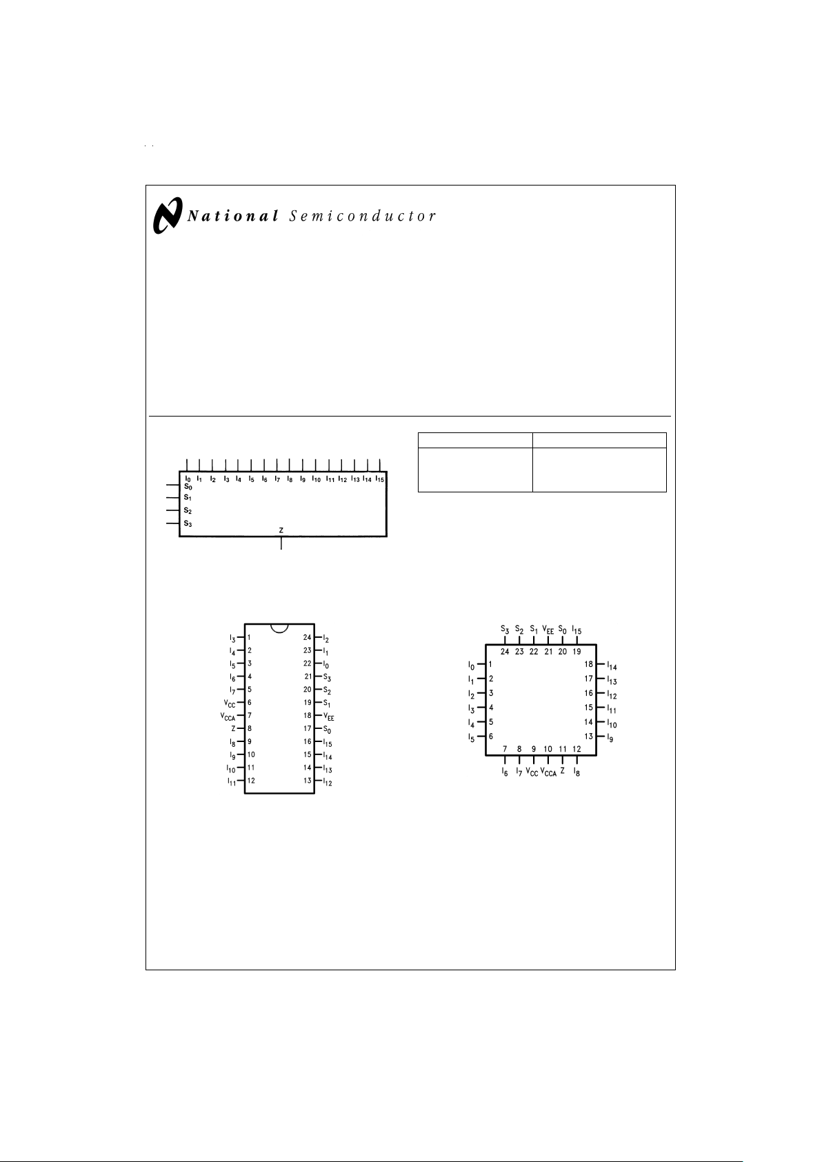
Logic Symbol
Pin Names Description
I
0–I15
Data Inputs
S
0–S3
Select Inputs
Z Data Output
Connection Diagrams
DS100301-1
24-Pin DIP
DS100301-2
24-Pin Quad Cerpak
DS100301-3
August 1998
100364 Low Power 16-Input Multiplexer
© 1998 National Semiconductor Corporation DS100301 www.national.com
Page 2
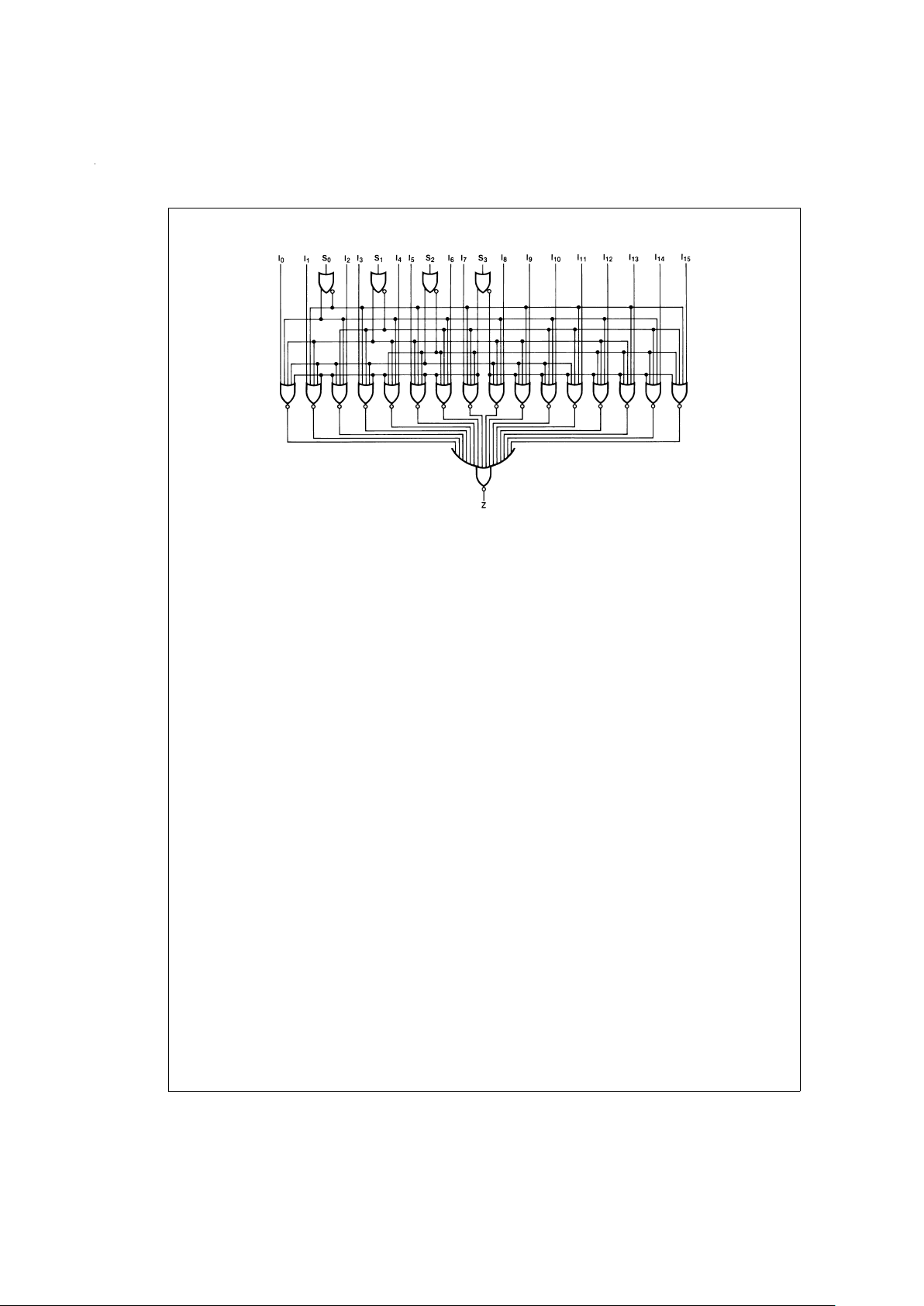
Logic Diagram
DS100301-5
www.national.com 2
Page 3
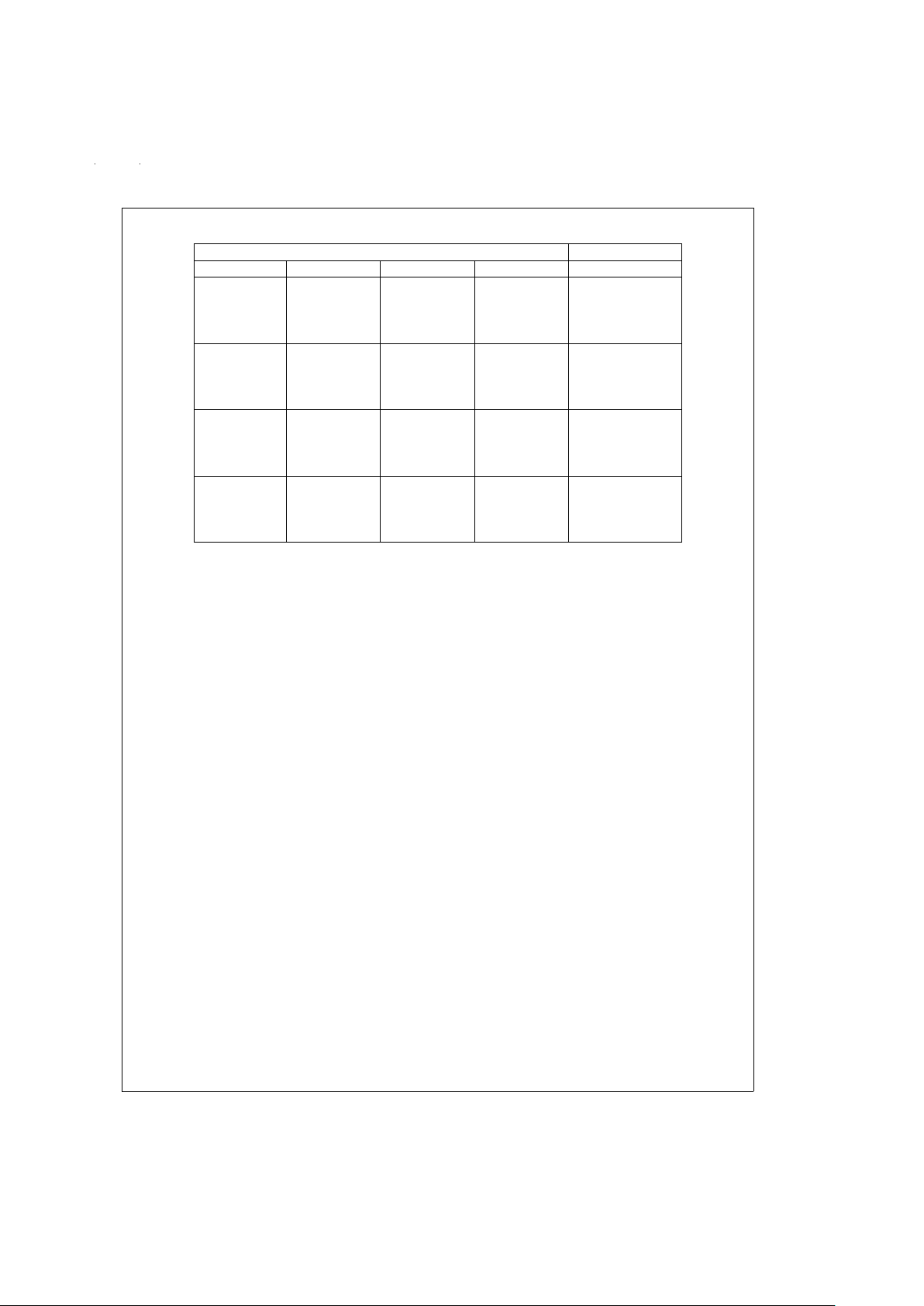
Truth Table
Select Inputs Output
S
0
S
1
S
2
S
3
Z
LLLL I
0
HLLL I
1
LHLL I
2
HHL L I
3
LLHL I
4
HLHL I
5
LHHL I
6
HHHL I
7
LLLH I
8
HLLH I
9
LHLH I
10
HHLH I
11
LLHH I
12
HLHH I
13
LHHH I
14
HHHH I
15
H=HIGH Voltage Level
L=LOW Voltage Level
www.national.com3
Page 4
Absolute Maximum Ratings (Note 1)
If Military/Aerospace specified devices are required,
please contact theNational Semiconductor Sales Office/
Distributors for availability and specifications.
Above which the useful life may be impaired
Storage Temperature (T
STG
) −65˚C to +150˚C
Maximum Junction Temperature (T
J
)
Ceramic +175˚C
Pin Potential to
Ground Pin (V
EE
) −7.0V to +0.5V
Input Voltage (DC) V
EE
to +0.5V
Output Current
(DC Output HIGH) −50 mA
ESD (Note 2) ≥ 2000V
Recommended Operating
Conditions
Case Temperature (TC)
Military −55˚C to +125˚C
Supply Voltage (V
EE
) −5.7V to −4.2V
Note 1: Absolute maximum ratings are those values beyond which the device may be damaged or have its useful life impaired. Functional operation
under these conditions is not implied.
Note 2: ESD testing conforms to MIL-STD-883, Method 3015.
Military Version
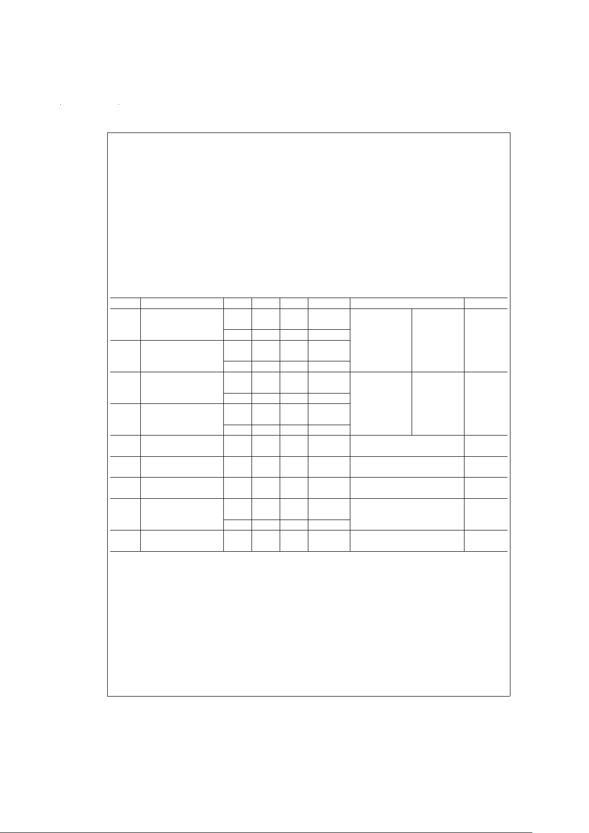
DC Electrical Characteristics
V
EE
=
−4.2V to −5.7V, V
CC
=
V
CCA
=
GND, T
C
=
−55˚C to +125˚C
Symbol Parameter Min Max Units T
C
Conditions Notes
V
OH
Output HIGH Voltage −1025 −870 mV 0˚C to V
IN
=
V
IH
(Max) Loading with (Notes 3, 4,
5)
+125˚C or V
IL
(Min) 50Ω to −2.0V
−1085 −870 mV −55˚C
V
OL
Output LOW Voltage −1830 −1620 mV 0˚C to
+125˚C
−1830 −1555 mV −55˚C
V
OHC
Output HIGH Voltage −1035 mV 0˚C to V
IN
=
V
IH
(Min) Loading with (Notes 3, 4,
5)
+125˚C or V
IL
(Max) 50Ω to −2.0V
−1085 mV −55˚C
V
OLC
Output LOW Voltage −1610 mV 0˚C to
+125˚C
−1555 mV −55˚C
V
IH
Input HIGH Voltage −1165 −870 mV −55˚C to Guaranteed HIGH Signal (Notes 3, 4,
5, 6)
+125˚C for All Inputs
V
IL
Input LOW Voltage −1830 −1475 mV −55˚C to Guaranteed LOW Signal (Notes 3, 4,
5, 6)
+125˚C for All Inputs
I
IL
Input LOW Current 0.50 µA −55˚C to V
EE
=
−4.2V (Notes 3, 4,
5)
+125˚C V
IN
=
V
IL
(Min)
I
IH
Input HIGH Current 300 µA 0˚C to V
EE
=
−5.7V (Notes 3, 4,
5)
+125˚C V
IN
=
V
IH
(Max)
450 µA −55˚C
I
EE
Power Supply Current −95 −35 mA −55˚C to Inputs Open (Notes 3, 4,
5)
+125˚C
Note 3: F100K 300 Series cold temperature testing is performed by temperature soaking (to guarantee junction temperature equals −55˚C), then testing immediately
without allowing for the junction temperature to stabilize due to heat dissipation after power-up. This provides “cold start” specs which can be considered a worst case
condition at cold temperatures.
Note 4: Screen tested 100%on each device at −55˚C, +25˚C, and +125˚C, Subgroups, 1, 2, 3, 7 and 8.
Note 5: Sampled tested (Method 5005, TableI) on each manufactured lot at −55˚C, +25˚C, and +125˚C, Subgroups A1, 2, 3, 7 and 8.
Note 6: Guaranteed by applying specified input condition and testing V
OH/VOL
.
www.national.com 4
Page 5
AC Electrical Characteristics
V
EE
=
−4.2V to −5.7V, V
CC
=
V
CCA
=
GND
Symbol Parameter T
C
=
−55˚C T
C
=
25˚C T
C
=
+125˚C Units Conditions Notes
Min Max Min Max Min Max
t
PLH
Propagation Delay 0.50 2.60 0.60 2.40 0.60 2.80 ns
Figures 1,
2
(Notes 7,
8, 9)
t
PHL
I0–I15to Output
t
PLH
Propagation Delay 0.70 3.30 0.90 3.10 1.00 3.50 ns
t
PHL
S0,S1to Output
t
PLH
Propagation Delay 0.50 2.90 0.70 2.60 0.60 3.00 ns
t
PHL
S2,S3to Output
t
TLH
Transition Time 0.20 1.20 0.20 1.20 0.20 1.20
ns
(Note 10)
t
THL
20%to 80%,80%to 20
%
Note 7: F100K 300 Series cold temperature testing is performed by temperature soaking (to guarantee junction temperature equals −55˚C), then testing immediately
without allowing for the junction temperature to stabilize due to heat dissipation after power-up. This provides “cold start” specs which can be considered a worst case
condition at cold temperatures.
Note 8: Screen tested 100%on each device at +25˚C, temperature only, Subgroup A9.
Note 9: Sample tested (Method 5005, TableI) on each Mfg. lot at +25˚C, Subgroup A9, and at +125˚C, and −55˚C temp., Subgroups A10 and A11.
Note 10: Not tested at +25˚C, +125˚C and −55˚C temperature (design characterization data).
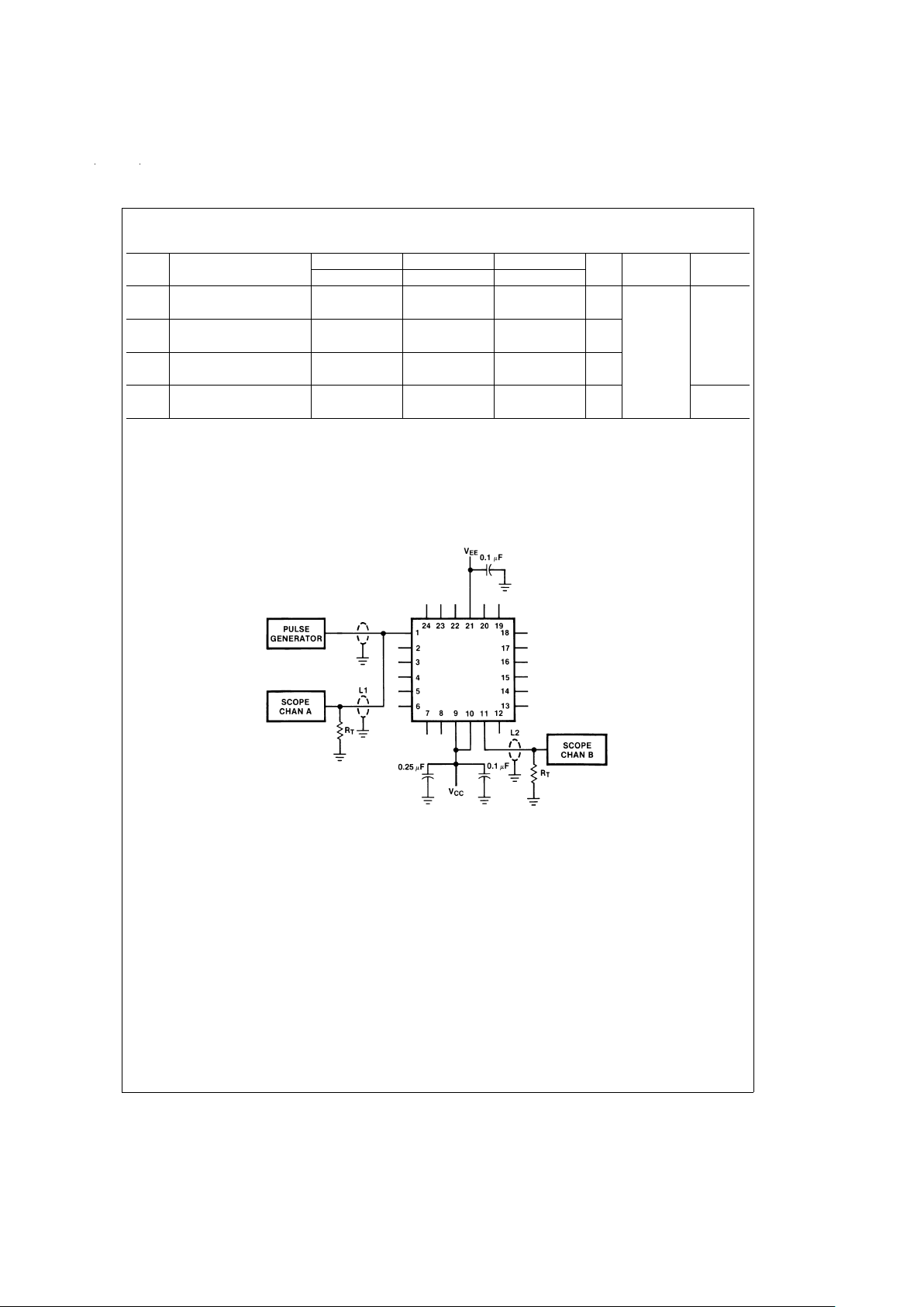
Test Circuit
DS100301-6
FIGURE 1. AC Test Circuit
www.national.com5
Page 6
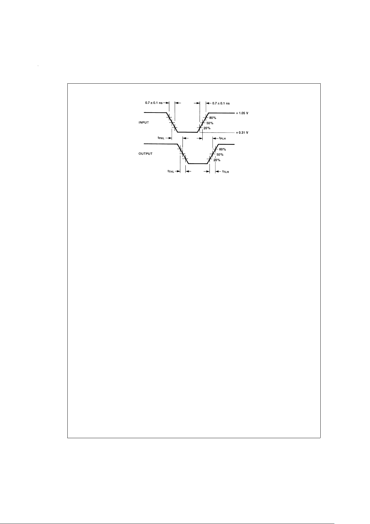
Switching Waveforms
DS100301-7
Note 11: VCC,V
CCA
=
+2V, V
EE
=
−2.5V
Note 12: L1 and L2=Equal length 50Ω impedance lines
Note 13: R
T
=
50Ω terminator internal to scope
Note 14: Decoupling 0.1 µF from GND to V
CC
and V
EE
Note 15: All unused outputs are loaded with 50Ω to GND
Note 16: C
L
=
Fixture and stray capacitance ≤ 3pF
Note 17: Pin numbers shown are for flatpak; for DIP see logic symbol
FIGURE 2. Propagation Delay and Transition Times
www.national.com 6
Page 7
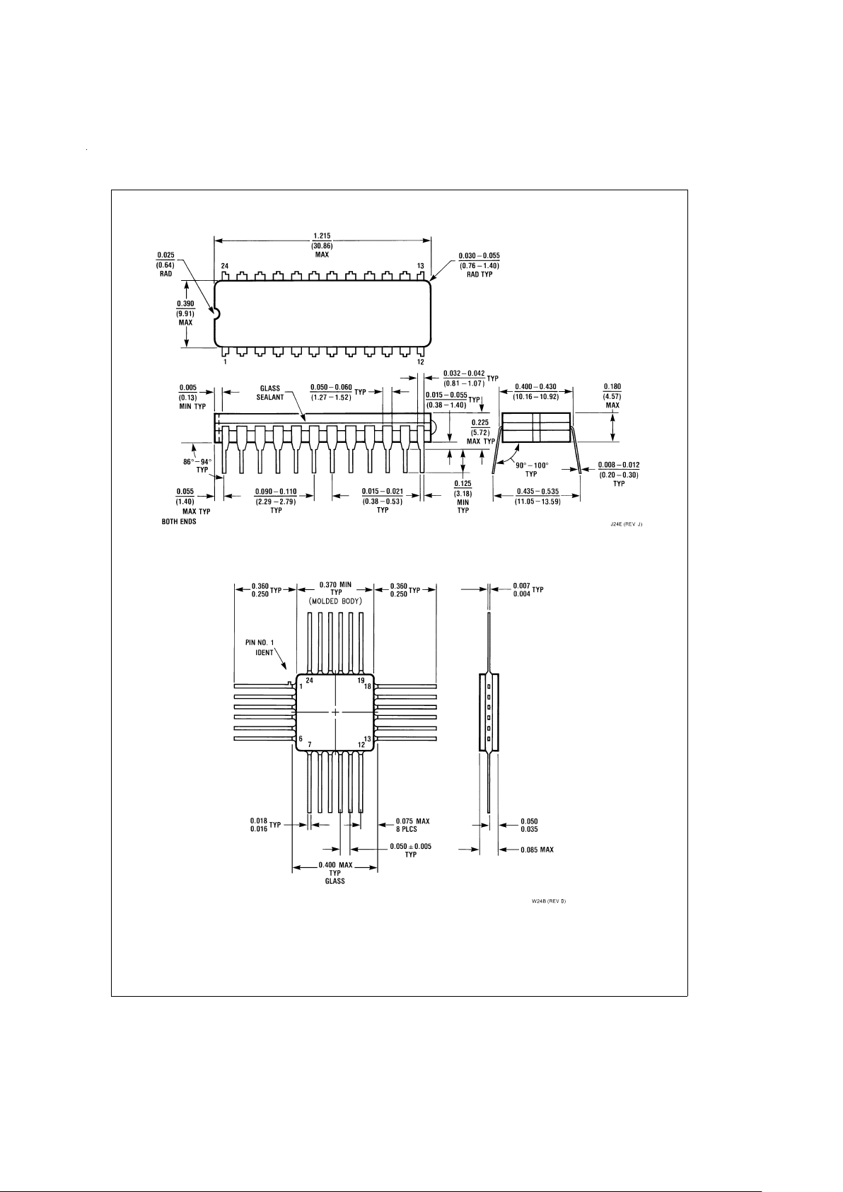
Physical Dimensions inches (millimeters) unless otherwise noted
24-Lead Ceramic Dual-In-Line Package (0.400" Wide) (D)
NS Package Number J24E
24-Lead Quad Cerpak (F)
NS Package Number W24B
www.national.com7
Page 8

LIFE SUPPORT POLICY
NATIONAL’S PRODUCTS ARE NOT AUTHORIZED FOR USE AS CRITICAL COMPONENTS IN LIFE SUPPORT DEVICES OR SYSTEMS WITHOUT THE EXPRESS WRITTEN APPROVAL OF THE PRESIDENT OF NATIONAL SEMICONDUCTOR CORPORATION. As used herein:
1. Life support devices or systems are devices or systems which, (a) are intended for surgical implant into
the body, or (b) support or sustain life, and whose failure to perform when properly used in accordance
with instructions for use provided in the labeling, can
be reasonably expected to result in a significant injury
to the user.
2. A critical component in any component of a life support
device or system whose failure to perform can be reasonably expected to cause the failure of the life support
device or system, or to affect its safety or effectiveness.
National Semiconductor
Corporation
Americas
Tel: 1-800-272-9959
Fax: 1-800-737-7018
Email: [email protected]
www.national.com
National Semiconductor
Europe
Fax: +49 (0) 1 80-530 85 86
Email: [email protected]
Deutsch Tel: +49 (0) 1 80-530 85 85
English Tel: +49 (0) 1 80-532 78 32
Français Tel: +49 (0) 1 80-532 93 58
Italiano Tel: +49 (0) 1 80-534 16 80
National Semiconductor
Asia Pacific Customer
Response Group
Tel: 65-2544466
Fax: 65-2504466
Email: [email protected]
National Semiconductor
Japan Ltd.
Tel: 81-3-5620-6175
Fax: 81-3-5620-6179
100364 Low Power 16-Input Multiplexer
National does not assume any responsibility for use of any circuitry described, no circuit patent licenses are implied and National reserves the right at any time without notice to change said circuitry and specifications.
 Loading...