

Page 1
54ABT377
Octal D-Type Flip-Flop with Clock Enable
General Description
The ’ABT377 has eight edge-triggered, D-type flip-flops with
individual D inputs and Q outputs. The common buffered
Clock (CP) input loadsallflip-flops simultaneously, when the
Clock Enable (CE) is LOW.
The register is fully edge-triggered. The state of each D input, one setup time before the LOW-to-HIGH clock transition, is transferred to the corresponding flip-flop’s Q output.
The CE input must be stable only one setup time prior to the
LOW-to-HIGH clock transition for predictable operation.
Features
n Clock enable for address and data synchronization
applications
Ordering Code:
Military Package Package Description
Number
54ABT377J-QML J20A 20-Lead Ceramic Dual-In-Line
54ABT377W-QML W20A 20-Lead Cerpack
54ABT377E-QML E20A 20-Lead Ceramic Leadless Chip Carrier, Type C
n Eight edge-triggered D flip-flops
n Buffered common clock
n See ’ABT273 for master reset version
n See ’ABT373 for transparent latch version
n See ’ABT374 for TRI-STATE
n Output sink capability of 48 mA, source capability of
24 mA
n Guaranteed latchup protection
n High impedance glitch free bus loading during entire
power up and power down cycle
n Non-destructive hot insertion capability
n Disable time less than enable time to avoid bus
contention
n Standard Microcircuit Drawing (SMD) 5962-9314801
®
version
54ABT377 Octal D-Type Flip-Flop with Clock Enable
July 1998
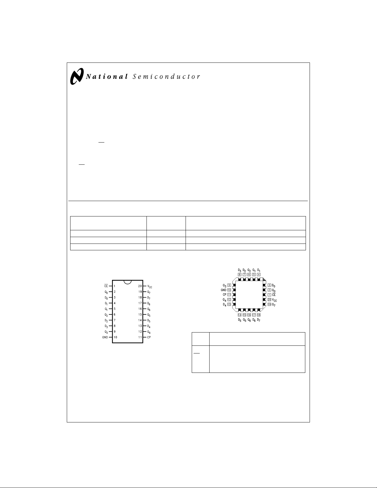
Connection Diagram
Pin Assignment for
DIP and Cerpack
Pin
DS100216-1
TRI-STATE®is a registered trademark of National Semiconductor Corporation.
© 1998 National Semiconductor Corporation DS100216 www.national.com
Names
D
0–D7
CE
CP Clock Pulse Input
Q
0–Q7
Pin Assignment for LCC
DS100216-11
Description
Data Inputs
Clock Enable (Active LOW)
Data Outputs
Page 2
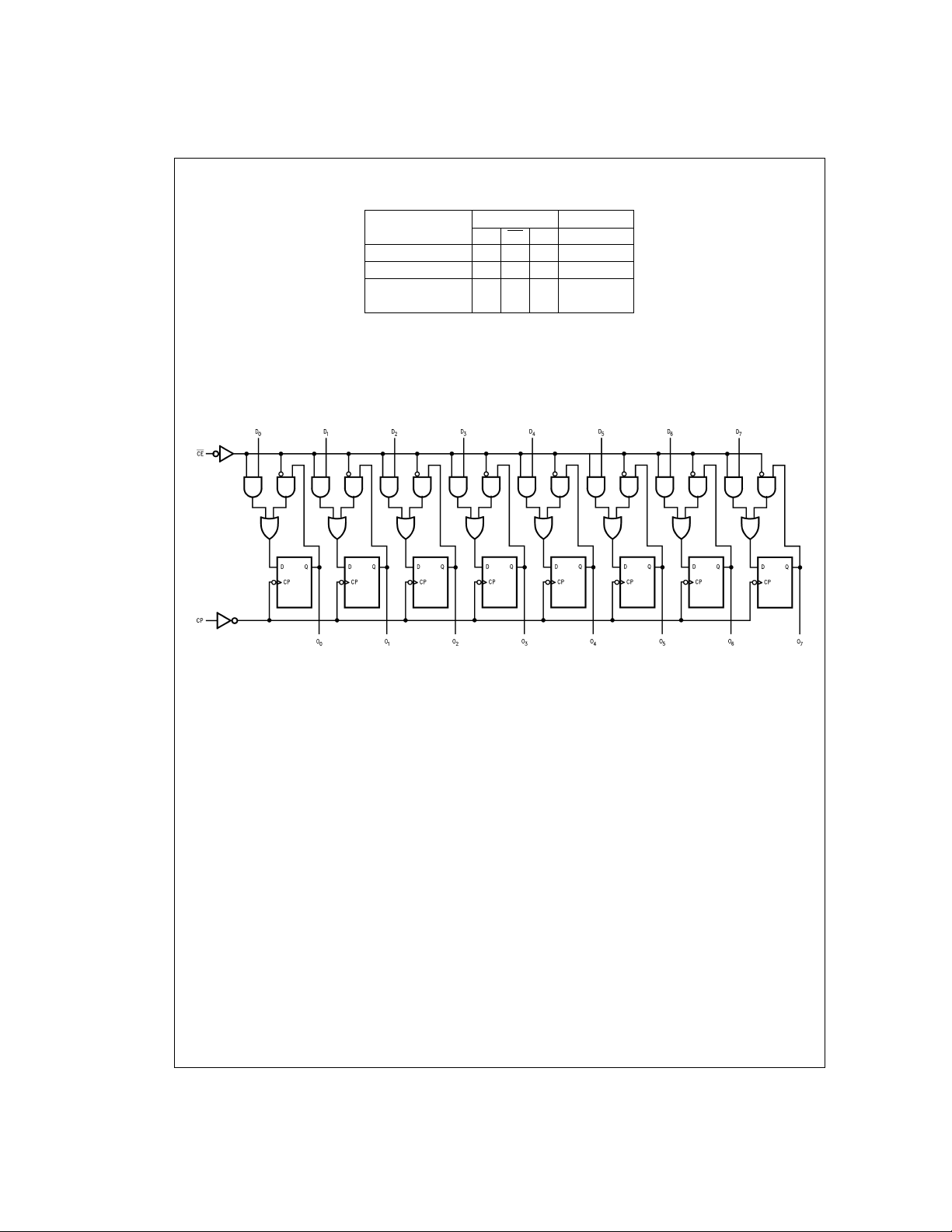
Truth Table
Logic Diagram
Mode Select-Function Table
Operating Mode Inputs Output
CP CE
D
Q
n
n
Load “1” I h H
Load “0” I I L
Hold h X No Change
(Do Nothing) X H X No Change
H=HIGH Voltage Level
h=HIGH Voltage Level one setup time prior to the LOW-to-HIGH Clock Transition
L=LOW Voltage Level
I=LOW Voltage Level one setup time prior to the LOW-to-HIGH Clock Transition
X=Immaterial
=
LOW-to-HIGH Clock Transition
Please note that this diagram is provided only for the understanding of logic operations and should not be used to estimate propagation delays.
www.national.com 2
DS100216-3
Page 3
Absolute Maximum Ratings (Note 1)
Storage Temperature −65˚C to +150˚C
Ambient Temperature under Bias −55˚C to +125˚C
Junction Temperature under Bias
Ceramic −55˚C to +175˚C
Pin Potential to
V
CC
Ground Pin −0.5V to +7.0V
Input Voltage (Note 2) −0.5V to +7.0V
Input Current (Note 2) −30 mA to +5.0 mA
Voltage Applied to Any Output
in the Disabled or
Power-Off State −0.5V to +4.75V
in the HIGH State −0.5V to V
DC Latchup Source Current −500 mA
(Across Comm Operating Range)
Over Voltage Latchup V
Recommended Operating
Conditions
Free Air Ambient Temperature
Military −55˚C to +125˚C
Supply Voltage
Military +4.5V to +5.5V
Minimum Input Edge Rate (∆V/∆t)
Data Input 50 mV/ns
CC
Enable Input 20 mV/ns
CC
Current Applied to Output
in LOW State (Max) Twice the rated I
(mA)
OL
DC Electrical Characteristics
Symbol Parameter ABT377 Units V
CC
Min Typ Max
V
V
V
V
V
I
I
Input HIGH Voltage 2.0 V Recognized HIGH Signal
IH
Input LOW Voltage 0.8 V Recognized LOW Signal
IL
Input Clamp Diode Voltage −1.2 V Min I
CD
Output HIGH Voltage 54ABT 2.5 V Min I
OH
54ABT 2.0 I
Output LOW Voltage 54ABT 0.55 V Min I
OL
Input HIGH Current 5 µA Max V
IH
5V
Input HIGH Current 7 µA Max V
BVI
IN
OH
OH
OL
IN
IN
IN
Breakdown Test
I
V
Input LOW Current −5 µA Max V
IL
−5 V
Input Leakage Test 4.75 V 0.0 I
ID
IN
IN
ID
All Other Pins Grounded
I
I
I
I
I
Output Short-Circuit Current −100 −275 mA Max V
OS
Output High Leakage Current 50 µA Max V
CEX
Power Supply Current 50 µA Max All Outputs HIGH
CCH
Power Supply Current 30 mA Max All Outputs LOW
CCL
Maximum ICC/Input Outputs Enabled V
CCT
OUT
OUT
I
1.5 mA Max Data Input V
All Others at V
I
CCD
Dynamic I
CC
No Load 0.3 mA/ Max Outputs Open (Note 3)
MHz One bit Toggling, 50%Duty Cycle
Note 1: Absolute maximum ratings are values beyond which the device may be damaged or have its useful life impaired. Functional operation under these conditions
is not implied.
Note 2: Either voltage limit or current limit is sufficient to protect inputs.
Note 3: For 8 bits toggling, I
Note 4: Guaranteed but not tested.
CCD
<
0.5 mA/MHz.
=
−18 mA
=
−3 mA
=
−24 mA
=
48 mA
=
2.7V (Note 4)
=
V
CC
=
7.0V
=
0.5V (Note 4)
=
0.0V
=
1.9 µA
=
0.0V
=
V
CC
=
− 2.1V
V
CC
Conditions
=
− 2.1V
V
I
CC
or GND
CC
+ 4.5V
3 www.national.com
Page 4
AC Electrical Characteristics
Symbol Parameter 54ABT Units
=
T
−55˚C to +125˚C
A
=
V
4.5V to 5.5V
CC
=
C
50 pF
L
Min Max
f
max
Max Clock 150 MHz
Frequency
t
PLH
t
PHL
Propagation Delay 2.2 6.0 ns
CP to O
n
2.8 6.8
AC Operating Requirements
54ABT
=
T
−55˚C to +125˚C
A
Symbol Parameter V
Min Max
t
(H) Setup Time, HIGH 2.0 ns
s
t
(L) or LOW Dnto CP 2.0
s
t
(H) Hold Time, HIGH 1.8 ns
h
t
(L) or LOW Dnto CP 1.8
h
t
(H) Setup Time, HIGH 3.0 ns
s
t
(L) or LOW CE to CP 3.0
s
t
(H) Hold Time, HIGH 1.0 ns
h
t
(L) or LOW CE to CP 1.0
h
t
(H) Pulse Width, CP, 3.3 ns
w
t
(L) HIGH or LOW 3.3
w
=
4.5V to 5.5V Units
CC
=
C
50 pF
L
Capacitance
Symbol Parameter Typ Units Conditions
C
IN
C
(Note 5) Output Capacitance 9 pF V
OUT
Note 5: C
www.national.com 4
is measured at frequency f=1 MHz, per MIL-STD-883B, Method 3012.
OUT
Input Capacitance 5 pF V
=
CC
=
CC
0V, T
5.0V
=
25˚C
A
Page 5

AC Loading
*Includes jig and probe capacitance
DS100216-4
FIGURE 1. Standard AC Test Load
FIGURE 2. V
=
1.5V
M
Input Pulse Requirements
Amplitude Rep. Rate t
w
t
r
3.0V 1 MHz 500 ns 2.5 ns 2.5 ns
FIGURE 3. Test Input Signal Requirements
DS100216-6
t
f
DS100216-5
FIGURE 5. Propagation Delay,
Pulse Width Waveforms
DS100216-9
FIGURE 6. Setup Time, Hold Time
and Recovery Time Waveforms
DS100216-8
FIGURE 4. Propagation Delay Waveforms for
Inverting and Non-Inverting Functions
5 www.national.com
Page 6
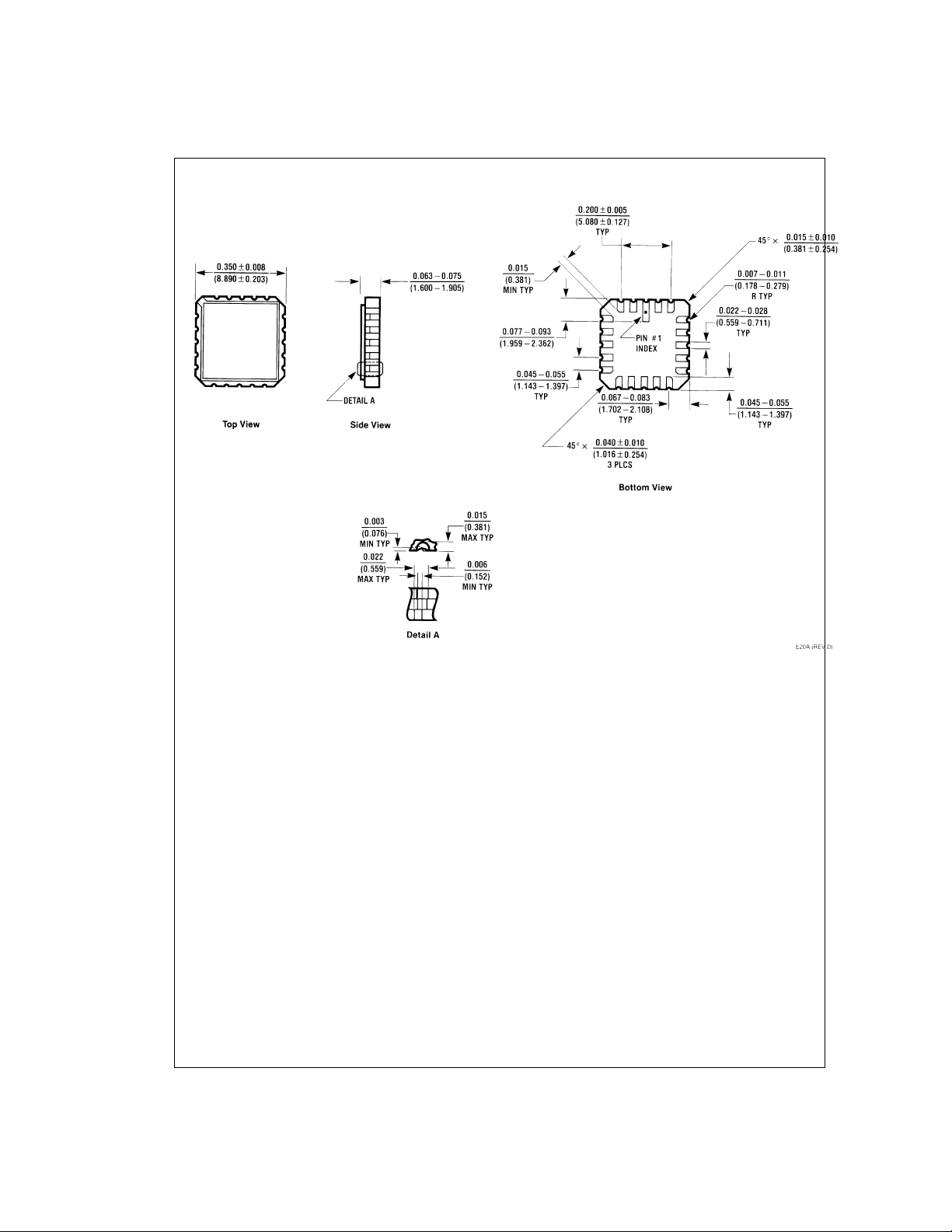
Physical Dimensions inches (millimeters) unless otherwise noted
20-Lead Ceramic Chip Carrier
NS Package Number E20A
www.national.com 6
Page 7
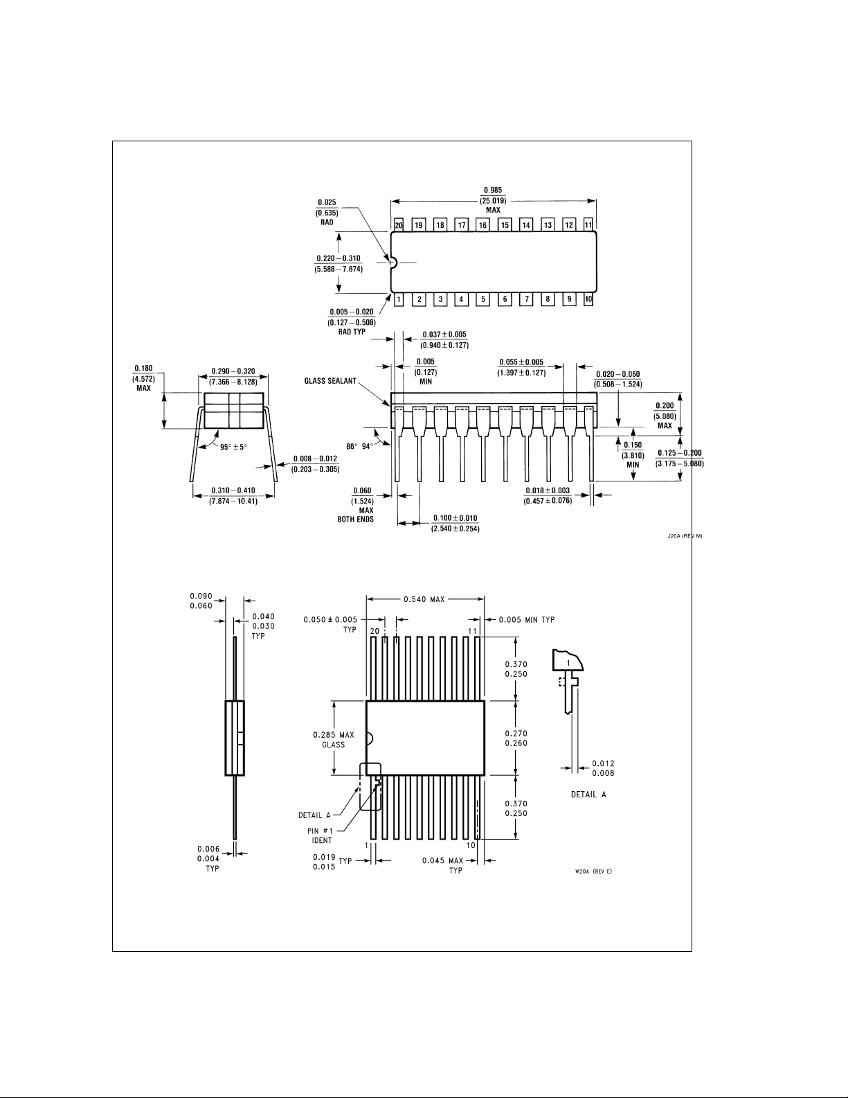
Physical Dimensions inches (millimeters) unless otherwise noted (Continued)
20-Lead Ceramic Dual-In-Line Package
NS Package Number J20A
20-Lead Ceramic Flatpack
NS Package Number W20A
7 www.national.com
Page 8

54ABT377 Octal D-Type Flip-Flop with Clock Enable
LIFE SUPPORT POLICY
NATIONAL’S PRODUCTS ARE NOT AUTHORIZED FOR USE AS CRITICAL COMPONENTS IN LIFE SUPPORT DEVICES OR SYSTEMS WITHOUT THE EXPRESS WRITTEN APPROVAL OF THE PRESIDENT OF NATIONAL SEMICONDUCTOR CORPORATION. As used herein:
1. Life support devices or systems are devices or systems which, (a) are intended for surgical implant into
the body, or (b) support or sustain life, and whose failure to perform when properly used in accordance
with instructions for use provided in the labeling, can
be reasonably expected to result in a significant injury
to the user.
National Semiconductor
Corporation
Americas
Tel: 1-800-272-9959
Fax: 1-800-737-7018
Email: [email protected]
www.national.com
National does not assume any responsibility for use of any circuitry described, no circuit patent licenses are implied and National reserves the right at any time without notice to change said circuitry and specifications.
National Semiconductor
Europe
Fax: +49 (0) 1 80-530 85 86
Email: [email protected]
Deutsch Tel: +49 (0) 1 80-530 85 85
English Tel: +49 (0) 1 80-532 78 32
Français Tel: +49 (0) 1 80-532 93 58
Italiano Tel: +49 (0) 1 80-534 16 80
2. A critical component in any component of a life support
device or system whose failure to perform can be reasonably expected to cause the failure of the life support
device or system, or to affect its safety or effectiveness.
National Semiconductor
Asia Pacific Customer
Response Group
Tel: 65-2544466
Fax: 65-2504466
Email: [email protected]
National Semiconductor
Japan Ltd.
Tel: 81-3-5620-6175
Fax: 81-3-5620-6179
 Loading...