

Datasheet 5962-9218501VSA, 5962-9218501VRA, 5962-9218501V2A, 5962-9218501MSA, 5962-9218501M2A Datasheet (NSC)
...Page 1
54ACTQ241
Quiet Series Octal Buffer/Line Driver with TRI-STATE
®
Outputs
General Description
The ACTQ241 is an octal buffer and line driver designed to
be employed as a memory address driver, clock driver and
bus oriented transmitteror receiver which provides improved
PC board density.TheACTQ utilizes NSC Quiet Series technology to guarantee quiet output switching and improved dynamic threshold performance. FACT Quiet Series
™
features
GTO
™
output control and undershoot corrector in addition to
a split ground bus for superior performance.
Features
n ICCand IOZreduced by 50
%
n Guaranteed simultaneous switching noise level and
dynamic threshold performance
n Improved latch-up immunity
n TRI-STATE outputs drive bus lines or buffer memory
address registers
n Outputs source/sink 24 mA
n Faster prop delays than the standard ’AC/’ACT241
n 4 kV minimum ESD immunity (’ACTQ)
n Standard Microcircuit Drawing (SMD) 5962-92185
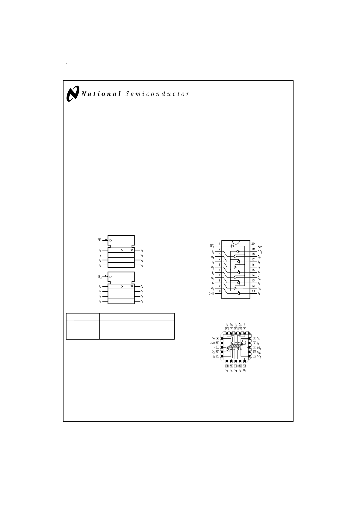
Logic Symbol
Pin Names Description
OE
1
,OE
2
TRI-STATE Output Enable Inputs
I
0–I7
Inputs
O
0–O7
Outputs
Connection Diagrams
GTO™is a trademark of National Semiconductor Corporation.
TRI-STATE
®
is a registered trademark of National Semiconductor Corporation.
FACT
®
is a registered trademark of Fairchild Semiconductor Corporation.
FACT Quiet Series
™
is a trademark of Fairchild Semiconductor Corporation.
IEEE/IEC
DS100246-1
Pin Assignment
for DIP and Flatpak
DS100246-2
Pin Assignment
for LCC
DS100246-3
August 1998
54ACTQ241 Quiet Series Octal Buffer/Line Driver with TRI-STATE Outputs
© 1998 National Semiconductor Corporation DS100246 www.national.com
Page 2
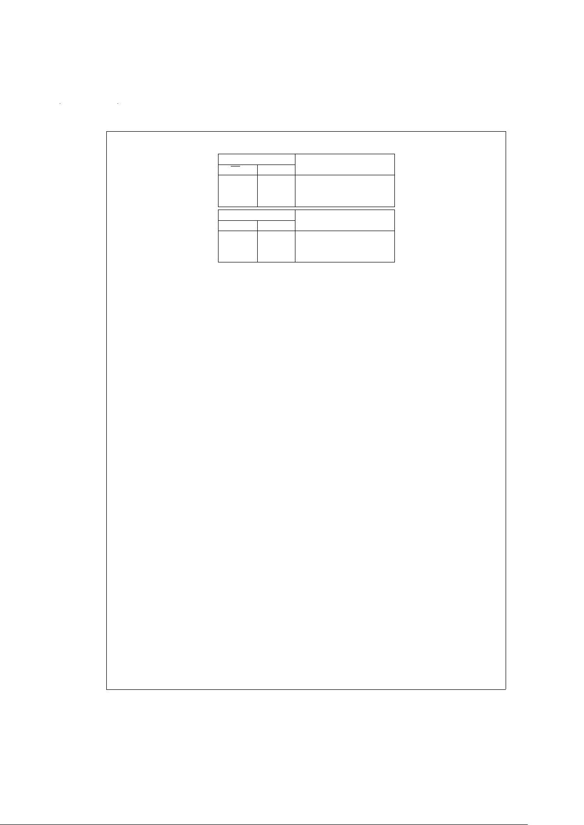
Truth Tables
Inputs Outputs
OE
1
I
n
(Pins 12, 14, 16, 18)
LL L
LH H
HX Z
Inputs Outputs
OE
2
I
n
(Pins 3, 5, 7, 9)
HL L
HH H
HX Z
H
=
HIGH Voltage Level
L=LOW Voltage Level
X=Immaterial
Z=High Impedance
www.national.com 2
Page 3
Absolute Maximum Ratings (Note 1)
If Military/Aerospace specified devices are required,
please contact the National Semiconductor Sales Office/
Distributors for availability and specifications.
Supply Voltage (V
CC
) −0.5V to +7.0V
DC Input Diode Current (I
IK
)
V
I
=
−0.5V −20 mA
V
I
=
V
CC
+ 0.5V +20 mA
DC Input Voltage (V
I
) −0.5V to VCC+ 0.5V
DC Output Diode Current (I
OK
)
V
O
=
−0.5V −20 mA
V
O
=
V
CC
+ 0.5V +20 mA
DC Output Voltage (V
O
) −0.5V to VCC+ 0.5V
DC Output Source
or Sink Current (I
O
)
±
50 mA
DC V
CC
or Ground Current
per Output Pin (I
CC
or I
GND
)
±
50 mA
Storage Temperature (T
STG
) −65˚C to +150˚C
DC Latch-Up Source or
Sink Current
±
300 mA
Junction Temperature (T
J
)
CDIP 175˚C
Recommended Operating
Conditions
Supply Voltage (VCC)
’ACTQ 4.5V to 5.5V
Input Voltage (V
I
) 0VtoV
CC
Output Voltage (VO) 0VtoV
CC
Operating Temperature (TA)
54ACTQ −55˚C to +125˚C
Minimum Input Edge Rate ∆V/∆t
’ACTQ Devices
V
IN
from 0.8V to 2.0V
V
CC
@
4.5V, 5.5V 125 mV/ns
Note 1: Absolute maximum ratings are those values beyond which damage
to the device may occur. The databook specifications should be met, without
exception, to ensure that the system design is reliable over its power supply,
temperature, and output/input loading variables. National does not recommend operation of FACT
®
circuits outside databook specifications.
Note 2: All commercial packaging is not recommended for applications requiring greater than 2000 temperature cycles from −40˚C to +125˚C.
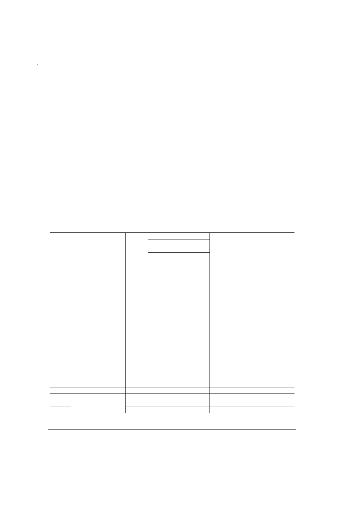
DC Electrical Characteristics for ’ACTQ Family Devices
54ACTQ
Symbol Parameter V
CC
T
A
=
Units Conditions
(V) −55˚C to +125˚C
Guaranteed Limits
V
IH
Minimum High Level 4.5 2.0 V V
OUT
=
0.1V
Input Voltage 5.5 2.0 or V
CC
− 0.1V
V
IL
Maximum Low Level 4.5 0.8 V V
OUT
=
0.1V
Input Voltage 5.5 0.8 or V
CC
− 0.1V
V
OH
Minimum High Level 4.5 4.4 V I
OUT
=
−50 µA
Output Voltage 5.5 5.4
(Note 3)
V
IN
=
V
IL
or V
IH
4.5 3.70 V I
OH
=
−24 mA
5.5 4.70 I
OH
=
−24 mA
V
OL
Maximum Low Level 4.5 0.1 V I
OUT
=
50 µA
Output Voltage 5.5 0.1
(Note 3)
V
IN
=
V
IL
or V
IH
4.5 0.50 V I
OL
=
24 mA
5.5 0.50 I
OL
=
24 mA
I
IN
Maximum Input 5.5
±
1.0 µA V
I
=
V
CC
, GND
Leakage Current
I
OZ
Maximum TRI-STATE 5.5
±
5.0 µA V
I
=
V
IL,VIH
Leakage Current V
O
=
V
CC
, GND
I
CCT
Maximum ICC/Input 5.5 1.6 mA V
I
=
V
CC
− 2.1V
(Note 4)
Minimum Dynamic
Output Current
I
OLD
5.5 50 mA V
OLD
=
1.65V Max
I
OHD
5.5 −50 mA V
OHD
=
3.85V Min
www.national.com3
Page 4

DC Electrical Characteristics for ’ACTQ Family Devices (Continued)
54ACTQ
Symbol Parameter V
CC
T
A
=
Units Conditions
(V) −55˚C to +125˚C
Guaranteed Limits
I
CC
Maximum Quiescent 5.5 80.0 µA V
IN
=
V
CC
Supply Current or GND (Note 5)
V
OLP
Quiet Output 5.0 1.5 V
Maximum Dynamic V
OL
(Notes 6, 7)
V
OLV
Quiet Output 5.0 −1.2 V
Minimum Dynamic V
OL
(Notes 6, 7)
Note 3: All outputs loaded; thresholds on input associated with output under test.
Note 4: Maximum test duration 2.0 ms, one output loaded at a time.
Note 5: I
CC
for 54ACTQ@25˚C is identical to 74ACTQ@25˚C.
Note 6: Plastic DIP package.
Note 7: Max number of outputs defined as (n). Data Inputs are driven 0V to 3V. One output
@
GND.
Note 8: Max number of Data Inputs (n) switching. n−1 Inputs switching 0V to 3V (’ACTQ). Input-under-test switching: 3V to threshold (V
ILD
), 0V to threshold (V
IHD
),
f=1 MHz.
AC Electrical Characteristics
54ACTQ
V
CC
T
A
=
−55˚C Fig.
Symbol Parameter (V) to +125˚C Units No.
(Note 9) C
L
=
50 pF
Min Max
t
PHL,tPLH
Propagation Delay 5.0 1.5 8.0 ns
Figure 4
Data to Output
t
PZL,tPZH
Output Enable Time 5.0 1.5 10.5 ns
Figure 5
t
PHZ,tPLZ
Output Disable Time 5.0 1.5 9.5 ns
Figure 5
Note 9: Voltage Range 5.0 is 5.0V±0.5V.
Note 10: Skew is defined as the absolute value of the difference between the actual propagation delay for any two separate outputs of the same device. The speci-
fication applies to any outputs switching in the same direction, either HIGH to LOW (t
OSHL
) or LOW to HIGH (t
OSLH
). Parameter guaranteed by design.
Capacitance
Symbol Parameter Typ Units Conditions
C
IN
Input Capacitance 4.5 pF V
CC
=
OPEN
C
PD
Power Dissipation 70 pF V
CC
=
5.0V
Capacitance
www.national.com 4
Page 5

AC Loading
AC Waveforms
DS100246-7
*Includes jig and probe capacitance
FIGURE 1. Standard AC Test Load
DS100246-8
FIGURE 2. Test Input Signal Levels
Amplitude Rep. Rate t
w
t
r
t
f
3.0V 1 MHz 500 ns 2.5 ns 2.5 ns
FIGURE 3. Test Input Signal Requirements
DS100246-9
FIGURE 4. Propagation Delay Waveforms for
Inverting and Non-Inverting Functions
DS100246-10
FIGURE 5. TRI-STATE Output HIGH and LOW
Enable and Disable Time
www.national.com5
Page 6

6
Page 7

Physical Dimensions inches (millimeters) unless otherwise noted
20-Terminal Ceramic Leadless Chip Carrier (L)
NS Package Number E20A
20-Lead Ceramic Dual-In-Line Package (D)
NS Package Number J20A
www.national.com7
Page 8

Physical Dimensions inches (millimeters) unless otherwise noted (Continued)
LIFE SUPPORT POLICY
NATIONAL’S PRODUCTS ARE NOT AUTHORIZED FOR USE AS CRITICAL COMPONENTS IN LIFE SUPPORT DEVICES OR SYSTEMS WITHOUT THE EXPRESS WRITTEN APPROVAL OF THE PRESIDENT OF NATIONAL SEMICONDUCTOR CORPORATION. As used herein:
1. Life support devices or systems are devices or systems which, (a) are intended for surgical implant into
the body, or (b) support or sustain life, and whose failure to perform when properly used in accordance
with instructions for use provided in the labeling, can
be reasonably expected to result in a significant injury
to the user.
2. A critical component in any component of a life support
device or system whose failure to perform can be reasonably expected to cause the failure of the life support
device or system, or to affect its safety or effectiveness.
National Semiconductor
Corporation
Americas
Tel: 1-800-272-9959
Fax: 1-800-737-7018
Email: support@nsc.com
www.national.com
National Semiconductor
Europe
Fax: +49 (0) 1 80-530 85 86
Email: europe.support@nsc.com
Deutsch Tel: +49 (0) 1 80-530 85 85
English Tel: +49 (0) 1 80-532 78 32
Français Tel: +49 (0) 1 80-532 93 58
Italiano Tel: +49 (0) 1 80-534 16 80
National Semiconductor
Asia Pacific Customer
Response Group
Tel: 65-2544466
Fax: 65-2504466
Email: sea.support@nsc.com
National Semiconductor
Japan Ltd.
Tel: 81-3-5620-6175
Fax: 81-3-5620-6179
20-Lead Ceramic Flatpak (F)
NS Package Number W20A
54ACTQ241 Quiet Series Octal Buffer/Line Driver with TRI-STATE Outputs
National does not assume any responsibility for use of any circuitry described, no circuit patent licenses are implied and National reserves the right at any time without notice to change said circuitry and specifications.
 Loading...