

Page 1
REVISIONS
LTR DESCRIPTION DATE (YR-MO-DA) APPROVED
A Correct notes to tests in table I and figure 1. Update drawing
requirements to MIL-PRF-38534.
01-06-14 Raymond Monnin
REV
SHEET
REV
SHEET
REV STATUS REV AAAAAAAAAAA
OF SHEETS
PMIC N/A PREPARED BY
STANDARD
MICROCIRCUIT
DRAWING
THIS DRAWING IS
AVAILABLE
FOR USE BY ALL
DEPARTMENTS
AND AGENCIES OF THE
DEPARTMENT OF DEFENSE
AMSC N/A
DSCC FORM 2233
APR 97
DISTRIBUTION STATEMENT A. Approved for public release; distribution is unlimited.
SHEET 1234567891011
Steve L. Duncan
CHECKED BY
Michael C. Jones
DEFENSE SUPPLY CENTER COLUMBUS
POST OFFICE BOX 3990
COLUMBUS, OHIO 43216-5000
http://www.dscc.dla.mil
APPROVED BY
Kendall A. Cottongim
MICROCIRCUIT, HYBRID, LINEAR, 90-VOLT
SYNCHRO TO DIGITAL CONVERTER
DRAWING APPROVAL DATE
93-01-19
REVISION LEVEL
A
SIZE
A
SHEET
CAGE CODE
67268
1 OF 11
5962-92054
5962-E332-01
Page 2
1. SCOPE
1.1 Scope. This drawing documents five product assurance classes as defined in paragraph 1.2.3 and MIL-PRF-38534. A
choice of case outlines and lead finishes which are available and are reflected in the Part or Identifying Number (PIN). When
available, a choice of radiation hardness assurance levels are reflected in the PIN.
1.2 PIN. The PIN shall be as shown in the following example:
5962 - 92054 01 H X X
Federal RHA Device Device Case Lead
stock class designator type class outline finish
designator (see 1.2.1) (see 1.2.2) designator (see 1.2.4) (see 1.2.5)
\ / (see 1.2.3)
\/
Drawing number
1.2.1 Radiation hardness assurance (RHA) designator. RHA marked devices shall meet the MIL-PRF-38534 specified RHA
levels and shall be marked with the appropriate RHA designator. A dash (-) indicates a non-RHA device.
1.2.2 Device type(s). The device type(s) identify the circuit function as follows:
Device type Generic number Circuit function Frequency Accuracy 1 LSB BIT/VEL
01 SDC-14612II-112 14-bit, 90 V S/D converter 400 Hz 4 min VEL
02 SDC-14612IIT-112 14-bit, 90 V S/D converter 400 Hz 4 min BIT
03 SDC-14614II-112 14-bit, 90 V S/D converter 60 Hz 4 min VEL
04 SDC-14614IIT-112 14-bit, 90 V S/D converter 60 Hz 4 min BIT
05 SDC-14617II-112 16-bit, 90 V S/D converter 400 Hz 4 min VEL
06 SDC-14617IIT-112 16-bit, 90 V S/D converter 400 Hz 4 min BIT
07 SDC-14619II-112 16-bit, 90 V S/D converter 60 Hz 4 min VEL
08 SDC-14619IIT-112 16-bit, 90 V S/D converter 60 Hz 4 min BIT
09 SDC-14617II-114 16-bit, 90 V S/D converter 400 Hz 2 min VEL
10 SDC-14617IIT -114 16-bit, 90 V S/D converter 400 Hz 2 min BIT
11 SDC-14619II-114 16-bit, 90 V S/D converter 60 Hz 2 min VEL
12 SDC-14619IIT-114 16-bit, 90 V S/D converter 60 Hz 2 min BIT
1.2.3 Device class designator. This device class designator shall be a single letter identifying the product assurance level.
All levels are defined by the requirements of MIL-PRF-38534 and require QML Certification as well as qualification (Class H, K,
and E) or QML Listing (Class G and D). The product assurance levels are as follows:
Device class Device performance documentation
K Highest reliability class available. This level is intended for use in space
applications.
H Standard military quality class level. This level is intended for use in applications
where non-space high reliability devices are required.
G Reduced testing version of the standard military quality class. This level uses the
Class H screening and In-Process Inspections with a possible limited temperature
range, manufacturer specified incoming flow, and the manufacturer guarantees (but
may not test) periodic and conformance inspections (Group A, B, C, and D).
E Designates devices which are based upon one of the other classes (K, H, or G)
D Manufacturer specified quality class. Quality level is defined by the manufacturers
internal, QML certified flow. This product may have a limited temperature range.
MICROCIRCUIT DRAWING
DEFENSE SUPPLY CENTER COLUMBUS
COLUMBUS, OHIO 43216-5000
DSCC FORM 2234
APR 97
STANDARD
with exception(s) taken to the requirements of that class. These exception(s) must
be specified in the device acquisition document; therefore the acquisition document
should be reviewed to ensure that the exception(s) taken will not adversely affect
system performance.
SIZE
A
REVISION LEVEL
A
5962-92054
SHEET
2
Page 3
1.2.4 Case outline(s). The case outline(s) are as designated in MIL-STD-1835 and as follows:
Outline letter Descriptive designator Terminals Package style
X See figure 1 36 Dual-in-line
1.2.5 Lead finish. The lead finish shall be as specified in MIL-PRF-38534.
1.3 Absolute maximum ratings. 1/
Positive supply voltage (VCC)..................................................... +7.0 V dc
Negative supply voltage (VEE).................................................... -7.0 V dc
Reference input voltage............................................................. 130 V rms
Digital input voltage range......................................................... -0.3 V dc to +7.0 V dc
Power dissipation, TA = +125C (PD) ......................................... 550 mW
Thermal resistance junction-to-case (
Thermal resistance junction-to-ambient (
Storage temperature range........................................................ -65C to +150C
Lead temperature (soldering, 10 seconds)................................ +300C
1.4 Recommended operating conditions.
Positive supply voltage (VCC)..................................................... +4.75 V dc to +5.25 V dc
Negative supply voltage (VEE).................................................... -4.75 V dc to -5.25 V dc
Reference input voltage range................................................... 10 V rms to 130 V rms
Reference input carrier frequency range:
Device types 01, 02, 05, 06, 09, and 10................................. 360 Hz to 5000 Hz
Device types 03, 04, 07, 08, 11, and 12................................. 47 Hz to 1000 Hz
Signal input voltage range......................................................... 81 V rms to 99 V rms
Ambient operating temperature range (TA)................................ -55C to +125C
2. APPLICABLE DOCUMENTS
JC).................................. 8.0C/W
JA)............................. 20C/W
2.1 Government specification, standards, and handbooks. The following specification, standards, and handbooks form a
part of this drawing to the extent specified herein. Unless otherwise specified, the issues of these documents are those listed in
the issue of the Department of Defense Index of Specifications and Standards (DoDISS) and supplement thereto, cited in the
solicitation.
SPECIFICATION
DEPARTMENT OF DEFENSE
MIL-PRF-38534 - Hybrid Microcircuits, General Specification for.
STANDARDS
DEPARTMENT OF DEFENSE
MIL-STD-883 - Test Method Standard Microcircuits.
MIL-STD-1835 - Interface Standard Electronic Component Case Outlines.
HANDBOOKS
DEPARTMENT OF DEFENSE
MIL-HDBK-103 - List of Standard Microcircuit Drawings.
MIL-HDBK-780 - Standard Microcircuit Drawings.
(Unless otherwise indicated, copies of the specification, standards, and handbooks are available from the Standardization
Document Order Desk, 700 Robbins Avenue, Building 4D, Philadelphia, PA 19111-5094.)
2.2 Order of precedence. In the event of a conflict between the text of this drawing and the references cited herein, the text
of this drawing takes precedence. Nothing in this document, however, supersedes applicable laws and regulations unless a
specific exemption has been obtained.
1/ Stresses above the absolute maximum ratings may cause permanent damage to the device. Extended operation at the
maximum levels may degrade performance and affect reliability.
MICROCIRCUIT DRAWING
DEFENSE SUPPLY CENTER COLUMBUS
COLUMBUS, OHIO 43216-5000
DSCC FORM 2234
APR 97
STANDARD
SIZE
A
REVISION LEVEL
A
5962-92054
SHEET
3
Page 4
3. REQUIREMENTS
3.1 Item requirements. The individual item performance requirements for device classes D, E, G, H, and K shall be in
accordance with MIL-PRF-38534. Compliance with MIL-PRF-38534 may include the performance of all tests herein or as
designated in the device manufacturer's Quality Management (QM) plan or as designated for the applicable device class.
Therefore, the tests and inspections herein may not be performed for the applicable device class (see MIL-PRF-38534).
Furthermore, the manufacturer may take exceptions or use alternate methods to the tests and inspections herein and not
perform them. However, the performance requirements as defined in MIL-PRF-38534 shall be met for the applicable device
class.
3.2 Design, construction, and physical dimensions. The design, construction, and physical dimensions shall be as specified
in MIL-PRF-38534 and herein.
3.2.1 Case outline(s). The case outline(s) shall be in accordance with 1.2.4 herein and figure 1.
3.2.2 Terminal connections. The terminal connections shall be as specified on figure 2.
3.2.3 Block diagram. The block diagram shall be as specified on figure 3.
3.3 Electrical performance characteristics. Unless otherwise specified herein, the electrical performance characteristics are
as specified in table I and shall apply over the full specified operating temperature range.
3.4 Electrical test requirements. The electrical test requirements shall be the subgroups specified in table II. The electrical
tests for each subgroup are defined in table I.
3.5 Marking of device(s). Marking of device(s) shall be in accordance with MIL-PRF-38534. The device shall be marked
with the PIN listed in 1.2 herein. In addition, the manufacturer's vendor similar PIN may also be marked in MIL-HDBK-103 and
QML-38534.
3.6 Data. In addition to the general performance requirements of MIL-PRF-38534, the manufacturer of the device described
herein shall maintain the electrical test data (variables format) from the initial quality conformance inspection group A lot
sample, for each device type listed herein. Also, the data should include a summary of all parameters manually tested, and for
those which, if any, are guaranteed. This data shall be maintained under document revision level control by the manufacturer
and be made available to the preparing activity (DSCC-VA) upon request.
3.7 Certificate of compliance. A certificate of compliance shall be required from a manufacturer in order to supply to this
drawing. The certificate of compliance (original copy) submitted to DSCC-VA shall affirm that the manufacturer's product meets
the performance requirements of MIL-PRF-38534 and herein.
3.8 Certificate of conformance. A certificate of conformance as required in MIL-PRF-38534 shall be provided with each lot of
microcircuits delivered to this drawing.
4. QUALITY ASSURANCE PROVISIONS
4.1 Sampling and inspection. Sampling and inspection procedures shall be in accordance with MIL-PRF-38534 or as
modified in the device manufacturer's Quality Management (QM) plan. The modification in the QM plan shall not affect the
form, fit, or function as described herein.
4.2 Screening. Screening shall be in accordance with MIL-PRF-38534. The following additional criteria shall apply:
a. Burn-in test, method 1015 of MIL-STD-883.
(1) Test condition A, B, C, or D. The test circuit shall be maintained by the manufacturer under document revision level
control and shall be made available to either DSCC-VA or the acquiring activity upon request. Also, the test circuit
shall specify the inputs, outputs, biases, and power dissipation, as applicable, in accordance with the intent
specified in test method 1015 of MIL-STD-883.
(2) TA as specified in accordance with table I of method 1015 of MIL-STD-883.
b. Interim and final electrical test parameters shall be as specified in table II herein, except interim electrical parameter
tests prior to burn-in are optional at the discretion of the manufacturer.
MICROCIRCUIT DRAWING
DEFENSE SUPPLY CENTER COLUMBUS
COLUMBUS, OHIO 43216-5000
DSCC FORM 2234
APR 97
STANDARD
SIZE
A
REVISION LEVEL
A
5962-92054
SHEET
4
Page 5
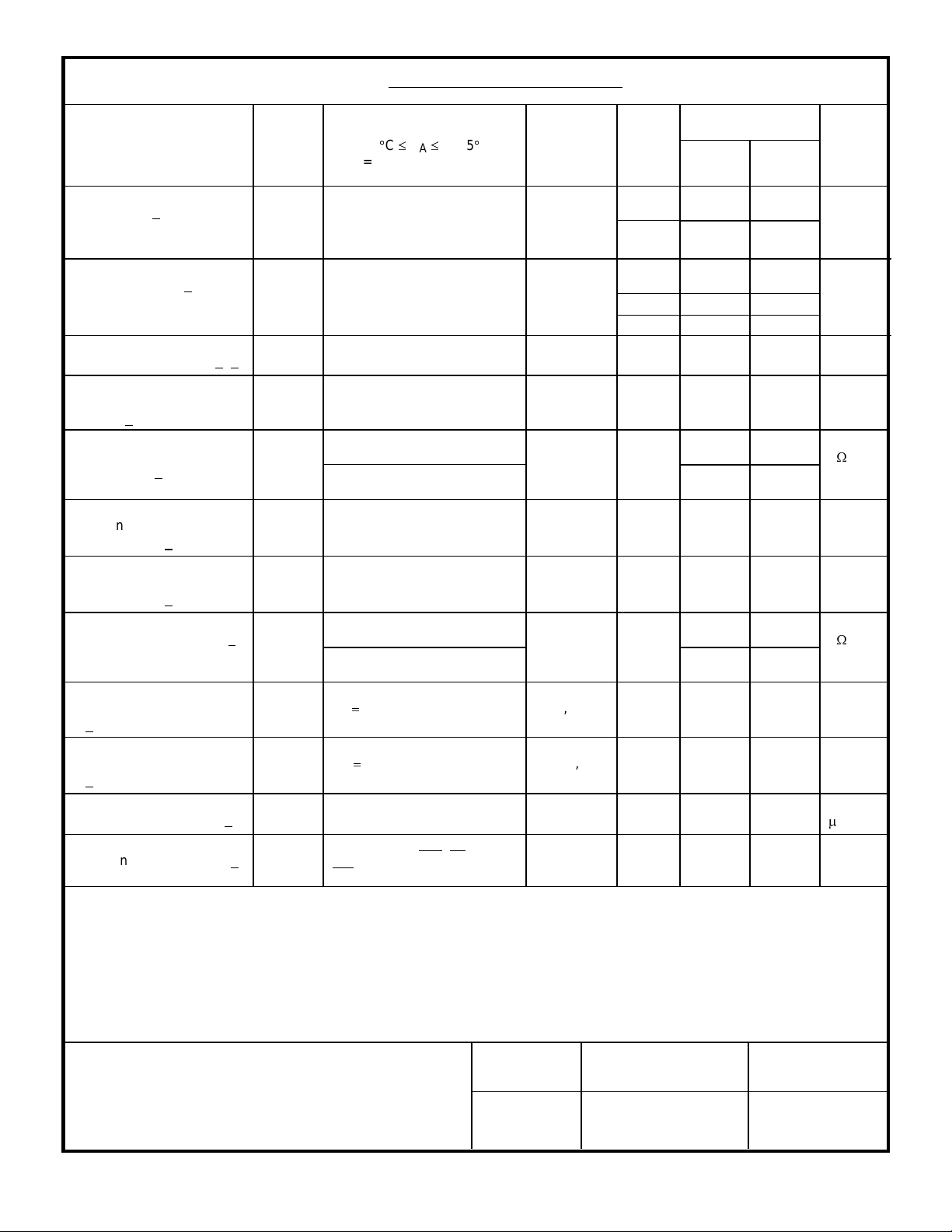
TABLE I. Electrical performance characteristics.
LimitsTest Symbol Conditions
Min Max
Unit
-55
C T
= +5 V dc, VEE = -5 V dc
V
CC
+125
A
C
Group A
subgroups
Device
type
unless otherwise specified
01-04 14Resolution 1/ RES 7,8A,8B
Bits
05-12 16
Output accuracy 2/ AOUT 7,8A,8B
01-04 -4 +4
LSB
05-08 -13 +13
09-12 -7 +7
Accuracy repeatability 2/ 3/ AR 7,8A,8B All -1.0 +1.0 LSB
Reference input voltage
V
IN1
4,5,6 All 10 130 V rms
range 3/
Z
IN1
Single ended 270Reference input
4,5,6 All
k
impedance 3/
Reference input common
Differential
V
CM1
4,5,6 All -200 +200 V pk
540
mode range 3/
Signal input common
mode range 3/
Digital output low voltage
1/
Digital output high voltage
1/
Output leakage current 3/ I
Digital input high voltage 1/ V
See footnotes at end of table.
V
CM2
IN2
Line-to-line 80Signal input impedance 3/ Z
Line-to-ground
V
OL
V
OH
OZ
IOL
IOH
-1.6 mA
0.4 mA
4,5,6 All -180 +180 V pk
4,5,6 All
k
123
1,2,3 All 0.4 V
1,2,3 All 2.8 V
1,2,3 All -60 +60
A
IH
Digital inputs INH, EL, and
EM. VIN = 2.0 V
1,2,3 All pass/
fail
MICROCIRCUIT DRAWING
DEFENSE SUPPLY CENTER COLUMBUS
COLUMBUS, OHIO 43216-5000
DSCC FORM 2234
APR 97
STANDARD
SIZE
A
REVISION LEVEL
A
5962-92054
SHEET
5
Page 6
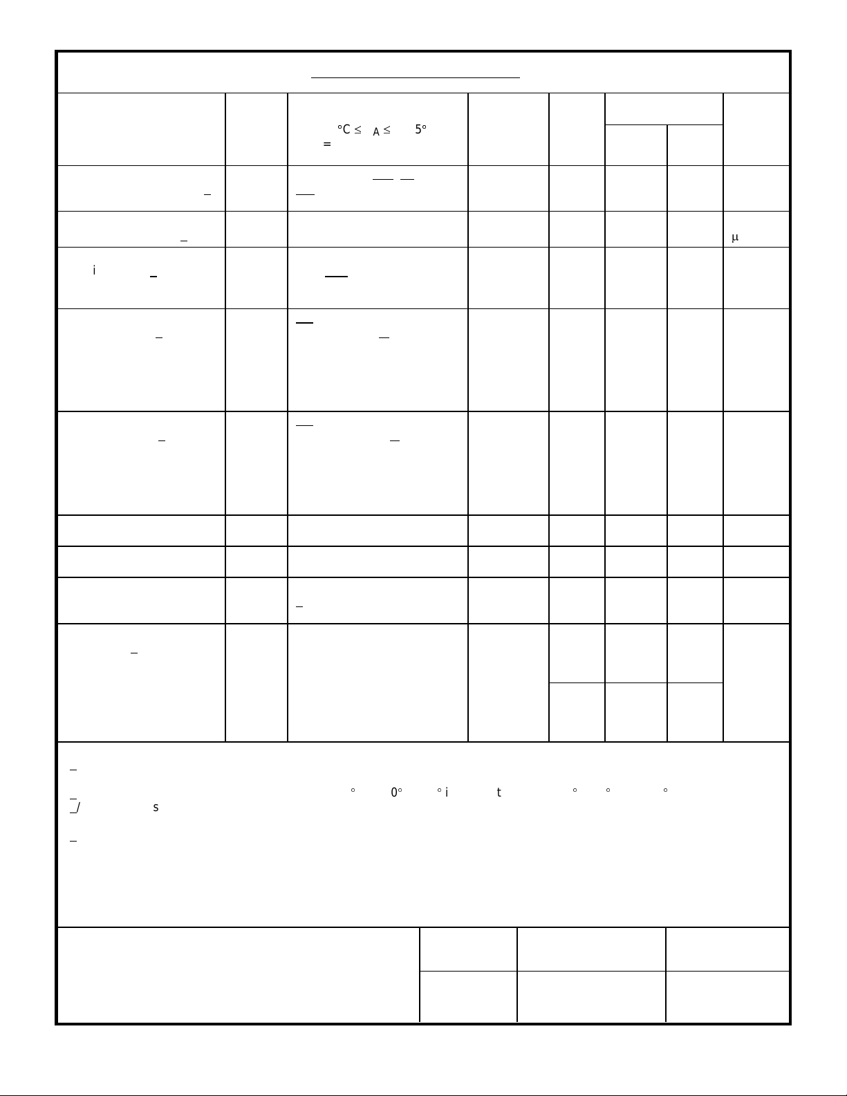
TABLE I. Electrical performance characteristics - Continued.
Digital input low voltage 1/ V
Digital input current 1/ I
Inhibit voltage 1/ V
Enable voltage 1/ V
Disable voltage 1/
(high impedance)
LimitsTest Symbol Conditions
Min Max
Unit
-55
C T
= +5 V dc, VEE = -5 V dc
V
CC
+125
A
C
Group A
subgroups
Device
type
unless otherwise specified
IL
Digital inputs INH, EL, and
EM. VIN = 0.8 V
IN
INH
Internal pull-up 4,5,6 All -10
No digital angles change
1,2,3 All pass/
fail
7,8A,8B All 0.8 V
A
while INH is logic 0 and
analog input is rotating
E
EM controls output bits 1
7,8A,8B All 0.8 V
through 8 and EL controls
output bits 9 through 14 for
device types 01 through 04,
and bits 9 through 16 for
device types 05 through 12.
V
D
EM controls output bits
7,8A,8B All 2.0 V
1 through 8 and EL controls
output bits 9 through 14 for
device types 01 through 04,
and bits 9 through 16 for
device types 05 through 12.
Positive supply voltage I
Negative supply voltage I
Analog velocity output
CC
EE
V
OUT
VCC = +5.25 V 1,2,3 All +17 mA
VEE = -5.25 V 1,2,3 All -17 mA
4/ 7,8A,8B All 3.24 4.00 V
voltage
Bandwidth 1/ BW 7,8A,8B
01,02,
72 134
Hz
05,06,
09,10
03,04,
10 20
07,08,
11,12
1/ These parameters are tested on a go-no-go basis only or in conjunction with other measured parameters and are not
directly testable.
2/ Output accuracy is measured at angles from 0, to 180, in 15 increments, and at 225, 270, and 315.
3/ Parameters shall be tested as part of device initial characterization and after design and process changes. Parameter
shall be guaranteed to the limits specified in table I for all lots not specifically tested.
4/ Analog output voltage is tested at 8 revolutions per second (rps) for device types 01 and 02, 1 rps for device types 03 and
04, 2 rps for device types 05, 06, 09, and 10, 0.25 rps for device types 07, 08, 11, and 12.
STANDARD
MICROCIRCUIT DRAWING
DEFENSE SUPPLY CENTER COLUMBUS
COLUMBUS, OHIO 43216-5000
SIZE
A
REVISION LEVEL
A
5962-92054
SHEET
6
DSCC FORM 2234
APR 97
Page 7
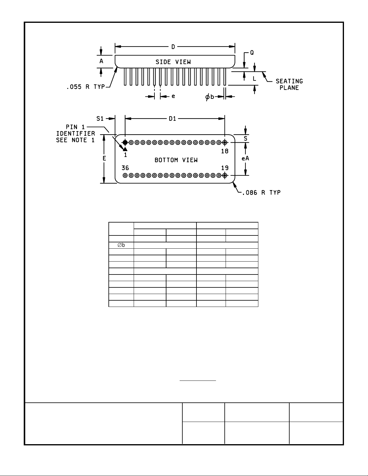
Case outline X.
Symbol
A --- 5.33 --- 0.210
b 0.46 TYP 0.018 TYP
D 48.01 48.26 1.890 1.900
D1 43.05 43.31 1.695 1.705
E 19.56 19.81 0.770 0.780
e 2.54 TYP 0.100 TYP
eA 15.11 15.37 0.595 0.605
L 5.84 --- 0.230 --Q --- 0.38 --- 0.015
S 2.03 2.54 0.080 0.100
S1 2.29 2.79 0.090 0.110
NOTES:
1.
Pin 1 is denoted by the contrasting colored bead and the ESD triangle on the under side.
2. Radius dimensions are in inches.
3. The U.S. government preferred system of measurement is the metric SI. This case outline was designed using inchpound units of measurement. In case of problems involving conflicts between the metric and inch-pound units, the
inch-pound units shall rule.
4. Pin number are for reference only.
5. Lead spacing dimensions apply only at seating plane.
Millimeters Inches
Minimum Maximum Minimum Maximum
FIGURE 1. Case outline(s).
MICROCIRCUIT DRAWING
DEFENSE SUPPLY CENTER COLUMBUS
COLUMBUS, OHIO 43216-5000
DSCC FORM 2234
APR 97
STANDARD
SIZE
A
REVISION LEVEL
A
5962-92054
SHEET
7
Page 8
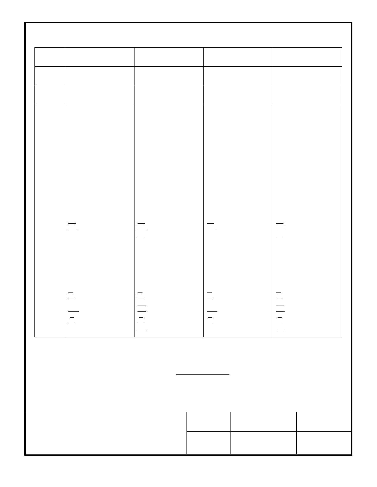
Device
types
01, 03 02, 04 05, 07, 09, 11 06, 08, 10, 12
Case
outline
Terminal
number
1
2
3
4
5
6
7
8
9
10
11
12
13
14
15
16
17
18
19
20
21
22
23
24
25
26
27
28
29
30
31
32
33
34
35
36
XXXX
Terminal symbol Terminal symbol Terminal symbol Terminal symbol
S1 A
S2 A
S3 A
No connection
GND
A GND
S1 B
S2 B
S3 B
No connection
V
(-5 V supply)
EE
V
(+5 V supply)
CC
S1 C
S2 C
S3 C
No connection
-REF
+REF
EM C
EL C
VEL C
Bit 1/9
Bit 2/10
Bit 3/11
Bit 4/12
Bit 5/13
Bit 6/14
Bit 7
Bit 8
EL B
EM B
VEL B
INH (inhibit)
EL A
EM A
VEL A
S1 A
S2 A
S3 A
No connection
GND
A GND
S1 B
S2 B
S3 B
No connection
V
(-5 V supply)
EE
V
(+5 V supply)
CC
S1 C
S2 C
S3 C
No connection
-REF
+REF
EM C
EL C
BIT C
Bit 1/9
Bit 2/10
Bit 3/11
Bit 4/12
Bit 5/13
Bit 6/14
Bit 7
Bit 8
EL B
EM B
BIT B
INH (inhibit)
EL A
EM A
BIT A
S1 A
S2 A
S3 A
No connection
GND
A GND
S1 B
S2 B
S3 B
No connection
V
(-5 V supply)
EE
V
(+5 V supply)
CC
S1 C
S2 C
S3 C
No connection
-REF
+REF
EM C
EL C
VEL C
Bit 1/9
Bit 2/10
Bit 3/11
Bit 4/12
Bit 5/13
Bit 6/14
Bit 7/15
Bit 8/16
EL B
EM B
VEL B
INH (inhibit)
EL A
EM A
VEL A
S1 A
S2 A
S3 A
No connection
GND
A GND
S1 B
S2 B
S3 B
No connection
V
(-5 V supply)
EE
V
(+5 V supply)
CC
S1 C
S2 C
S3 C
No connection
-REF
+REF
EM C
EL C
BIT C
Bit 1/9
Bit 2/10
Bit 3/11
Bit 4/12
Bit 5/13
Bit 6/14
Bit 7/15
Bit 8/16
EL B
EM B
BIT B
INH (inhibit)
EL A
EM A
BIT A
MICROCIRCUIT DRAWING
DEFENSE SUPPLY CENTER COLUMBUS
COLUMBUS, OHIO 43216-5000
DSCC FORM 2234
APR 97
STANDARD
FIGURE 2. Terminal connections.
SIZE
A
REVISION LEVEL
A
5962-92054
SHEET
8
Page 9
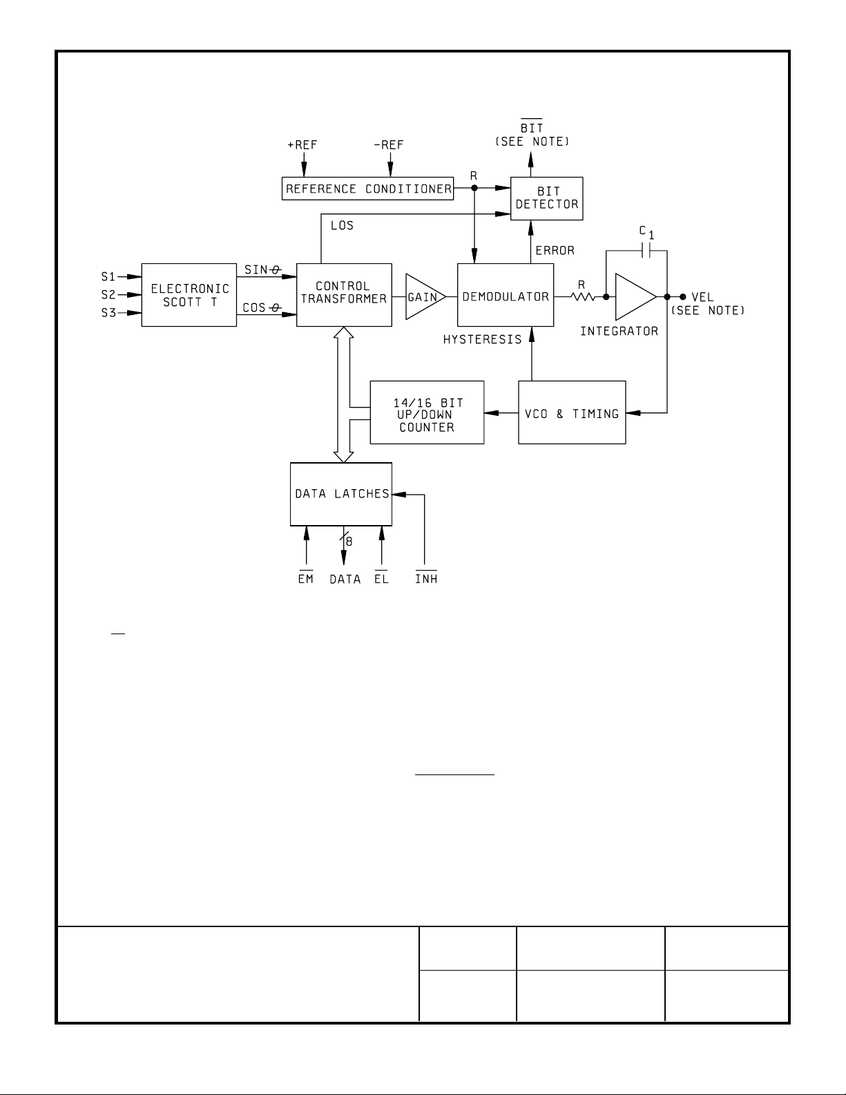
NOTE:
1. BIT is not connected on device types 01, 03, 05, 07, 09, and 11. VEL is not connected on device types 02, 04, 06, 08,
10, and 12.
FIGURE 3. Block diagram.
MICROCIRCUIT DRAWING
DEFENSE SUPPLY CENTER COLUMBUS
COLUMBUS, OHIO 43216-5000
DSCC FORM 2234
APR 97
STANDARD
SIZE
A
REVISION LEVEL
A
5962-92054
SHEET
9
Page 10
TABLE II. Electrical test requirements.
MIL-PRF-38534 test requirements Subgroups
(in accordance with
MIL-PRF-38534, group A
test table)
Interim electrical parameters 1,4,7
Final electrical parameters 1*,2,3,4,5,6,7,8A,8B
Group A test requirements 1,2,3,4,5,6,7,8A,8B
Group C end-point electrical
parameters
End-point electrical parameters
for radiation hardness assurance
(RHA) devices
* PDA applies to subgroup 1.
4.3 Conformance and periodic inspections. Conformance inspection (CI) and periodic inspection (PI) shall be in accordance
with MIL-PRF-38534 and as specified herein.
4.3.1 Group A inspection (CI). Group A inspection shall be in accordance with MIL-PRF-38534 and as follows:
a. Tests shall be as specified in table II herein.
b. Subgroups 9, 10, and 11 shall be omitted.
4.3.2 Group B inspection (PI). Group B inspection shall be in accordance with MIL-PRF-38534.
4.3.3 Group C inspection (PI). Group C inspection shall be in accordance with MIL-PRF-38534 and as follows:
a. End-point electrical parameters shall be as specified in table II herein.
b. Steady-state life test, method 1005 of MIL-STD-883.
(1) Test condition A, B, C, or D. The test circuit shall be maintained by the manufacturer under document revision level
control and shall be made available to either DSCC-VA or the acquiring activity upon request. Also, the test circuit
shall specify the inputs, outputs, biases, and power dissipation, as applicable, in accordance with the intent
specified in test method 1005 of MIL-STD-883.
1,2,3,4,5,6,7,8A,8B
Not applicable
(2) TA as specified in accordance with table I of method 1005 of MIL-STD-883.
(3) Test duration: 1,000 hours, except as permitted by method 1005 of MIL-STD-883.
4.3.4 Group D inspection (PI). Group D inspection shall be in accordance with MIL-PRF-38534.
4.3.5 Radiation Hardness Assurance (RHA) inspection. RHA inspection is not currently applicable to this drawing.
STANDARD
MICROCIRCUIT DRAWING
DEFENSE SUPPLY CENTER COLUMBUS
COLUMBUS, OHIO 43216-5000
DSCC FORM 2234
APR 97
SIZE
A
REVISION LEVEL
A
5962-92054
SHEET
10
Page 11
5. PACKAGING
5.1 Packaging requirements. The requirements for packaging shall be in accordance with MIL-PRF-38534.
6. NOTES
6.1 Intended use. Microcircuits conforming to this drawing are intended for use for Government microcircuit applications
(original equipment), design applications, and logistics purposes.
6.2 Replaceability. Microcircuits covered by this drawing will replace the same generic device covered by a contractor-
prepared specification or drawing.
6.3 Configuration control of SMD's. All proposed changes to existing SMD's will be coordinated with the users of record for
the individual documents. This coordination will be accomplished in accordance with MIL-PRF-38534.
6.4 Record of users. Military and industrial users shall inform Defense Supply Center Columbus when a system application
requires configuration control and the applicable SMD. DSCC will maintain a record of users and this list will be used for
coordination and distribution of changes to the drawings. Users of drawings covering microelectronic devices (FSC 5962)
should contact DSCC-VA, telephone (614) 692-0544.
6.5 Comments. Comments on this drawing should be directed to DSCC-VA, Post Office Box 3990, Columbus, Ohio 43216-
5000, or telephone (614) 692-0512.
6.6 Sources of supply. Sources of supply are listed in MIL-HDBK-103 and QML-38534. The vendors listed in MIL-HDBK-
103 and QML-38534 have submitted a certificate of compliance (see 3.7 herein) to DSCC-VA and have agreed to this drawing.
MICROCIRCUIT DRAWING
DEFENSE SUPPLY CENTER COLUMBUS
COLUMBUS, OHIO 43216-5000
DSCC FORM 2234
APR 97
STANDARD
SIZE
A
REVISION LEVEL
A
5962-92054
SHEET
11
Page 12

STANDARD MICROCIRCUIT DRAWING BULLETIN
DATE: 01-06-14
Approved sources of supply for SMD 5962-92054 are listed below for immediate acquisition information only and
shall be added to MIL-HDBK-103 and QML-38534 during the next revisions. MIL-HDBK-103 and QML-38534 will be
revised to include the addition or deletion of sources. The vendors listed below have agreed to this drawing and a
certificate of compliance has been submitted to and accepted by DSCC-VA. This bulletin is superseded by the next
dated revisions of MIL-HDBK-103 and QML-38534.
Standard
microcircuit drawing
PIN 1/
5962-9205401HXA
5962-9205401HXA
5962-9205401HXA
5962-9205401HXA
5962-9205401HXC
5962-9205401HXC
5962-9205401HXC
5962-9205401HXC
5962-9205402HXA
5962-9205402HXA
5962-9205402HXA
5962-9205402HXA
5962-9205402HXC
5962-9205402HXC
5962-9205402HXC
5962-9205402HXC
5962-9205403HXA
5962-9205403HXA
5962-9205403HXA
5962-9205403HXA
5962-9205403HXC
5962-9205403HXC
5962-9205403HXC
5962-9205403HXC
5962-9205404HXA
5962-9205404HXA
5962-9205404HXA
5962-9205404HXA
5962-9205404HXC
5962-9205404HXC
5962-9205404HXC
5962-9205404HXC
Vendor
CAGE
number
S7631
19645
S7631
19645
S7631
19645
S7631
19645
S7631
19645
S7631
19645
S7631
19645
S7631
19645
S7631
19645
S7631
19645
S7631
19645
S7631
19645
S7631
19645
S7631
19645
S7631
19645
S7631
19645
Vendor
similar
PIN 2/
SDC-14612II-152
SDC-14612II-152
SDC-14612II-142
SDC-14612II-142
SDC-14612II-132
SDC-14612II-132
SDC-14612II-112
SDC-14612II-112
SDC-14612IIT-152
SDC-14612IIT-152
SDC-14612IIT-142
SDC-14612IIT-142
SDC-14612IIT-132
SDC-14612IIT-132
SDC-14612IIT-112
SDC-14612IIT-112
SDC-14614II-152
SDC-14614II-152
SDC-14614II-142
SDC-14614II-142
SDC-14614II-132
SDC-14614II-132
SDC-14614II-112
SDC-14614II-112
SDC-14614IIT-152
SDC-14614IIT-152
SDC-14614IIT-142
SDC-14614IIT-142
SDC-14614IIT-132
SDC-14614IIT-132
SDC-14614IIT-112
SDC-14614IIT-112
5962-9205405HXA
5962-9205405HXA
5962-9205405HXA
5962-9205405HXA
5962-9205405HXC
5962-9205405HXC
5962-9205405HXC
5962-9205405HXC
See footnotes at end of table.
S7631
19645
S7631
19645
S7631
19645
S7631
19645
1 of 3
SDC-14617II-152
SDC-14617II-152
SDC-14617II-142
SDC-14617II-142
SDC-14617II-132
SDC-14617II-132
SDC-14617II-112
SDC-14617II-112
Page 13
STANDARD MICROCIRCUIT DRAWING BULLETIN - Continued.
DATE: 01-06-14
Standard
microcircuit drawing
PIN 1/
5962-9205406HXA
5962-9205406HXA
5962-9205406HXA
5962-9205406HXA
5962-9205406HXC
5962-9205406HXC
5962-9205406HXC
5962-9205406HXC
5962-9205407HXA
5962-9205407HXA
5962-9205407HXA
5962-9205407HXA
5962-9205407HXC
5962-9205407HXC
5962-9205407HXC
5962-9205407HXC
5962-9205408HXA
5962-9205408HXA
5962-9205408HXA
5962-9205408HXA
5962-9205408HXC
5962-9205408HXC
5962-9205408HXC
5962-9205408HXC
5962-9205409HXA
5962-9205409HXA
5962-9205409HXA
5962-9205409HXA
5962-9205409HXC
5962-9205409HXC
5962-9205409HXC
5962-9205409HXC
Vendor
CAGE
number
S7631
19645
S7631
19645
S7631
19645
S7631
19645
S7631
19645
S7631
19645
S7631
19645
S7631
19645
S7631
19645
S7631
19645
S7631
19645
S7631
196459
S7631
19645
S7631
19645
S7631
19645
S7631
19645
Vendor
similar
PIN 2/
SDC-14617IIT-152
SDC-14617IIT-152
SDC-14617IIT-142
SDC-14617IIT-142
SDC-14617IIT-132
SDC-14617IIT-132
SDC-14617IIT-112
SDC-14617IIT-112
SDC-14619II-152
SDC-14619II-152
SDC-14619II-142
SDC-14619II-142
SDC-14619II-132
SDC-14619II-132
SDC-14619II-112
SDC-14619II-112
SDC-14619IIT-152
SDC-14619IIT-152
SDC-14619IIT-142
SDC-14619IIT-142
SDC-14619IIT-132
SDC-14619IIT-132
SDC-14619IIT-112
SDC-14619IIT-112
SDC-14617II-154
SDC-14617II-154
SDC-14617II-144
SDC-14617II-144
SDC-14617II-134
SDC-14617II-134
SDC-14617II-114
SDC-14617II-114
5962-9205410HXA
5962-9205410HXA
5962-9205410HXA
5962-9205410HXA
5962-9205410HXC
5962-9205410HXC
5962-9205410HXC
5962-9205410HXC
5962-9205411HXA
5962-9205411HXA
5962-9205411HXA
5962-9205411HXA
5962-9205411HXC
5962-9205411HXC
5962-9205411HXC
5962-9205411HXC
See footnotes at end of table.
S7631
19645
S7631
19645
S7631
19645
S7631
19645
S7631
19645
S7631
19645
S7631
19645
S7631
19645
2 of 3
SDC-14617IIT-154
SDC-14617IIT-154
SDC-14617IIT-144
SDC-14617IIT-144
SDC-14617IIT-134
SDC-14617IIT-134
SDC-14617IIT-114
SDC-14617IIT-114
SDC-14619II-154
SDC-14619II-154
SDC-14619II-144
SDC-14619II-144
SDC-14619II-134
SDC-14619II-134
SDC-14619II-114
SDC-14619II-114
Page 14
STANDARD MICROCIRCUIT DRAWING BULLETIN - Continued.
DATE: 01-06-14
Standard
microcircuit drawing
PIN 1/
5962-9205412HXA
5962-9205412HXA
5962-9205412HXA
5962-9205412HXA
5962-9205412HXC
5962-9205412HXC
5962-9205412HXC
5962-9205412HXC
1/ The lead finish shown for each PIN representing a hermetic package is the most readily available from the
manufacturer listed for that part. If the desired lead finish is not listed contact the Vendor to determine its
availability.
2/ Caution. Do not use this number for item acquisition. Items acquired to this number may not satisfy the
performance requirements of this drawing.
Vendor CAGE Vendor name
number and address
S7631 DDC Ireland, LTD.
19645 Data Device Corporation
Vendor
CAGE
number
S7631
19645
S7631
19645
S7631
19645
S7631
19645
Vendor
similar
PIN 2/
SDC-14619IIT-154
SDC-14619IIT-154
SDC-14619IIT-144
SDC-14619IIT-144
SDC-14619IIT-134
SDC-14619IIT-134
SDC-14619IIT-114
SDC-14619IIT-114
Cork Business & Technology Park
Model Farm Road
Cork, Ireland
105 Wilbur Place
Bohemia, NY 11716-2482
The information contained herein is disseminated for convenience only and the
Government assumes no liability whatsoever for any inaccuracies in the
information bulletin.
3 of 3
 Loading...