

Page 1
54ACT818
8-Bit Diagnostic Register
General Description
The ’ACT818 is a high-speed, general-purpose pipeline register with an on-board diagnostic register for performing serial diagnostics and/or writable control store loading.
The D-to-Y path provides an 8-bit parallel data path pipeline
register for normal system operation.Thediagnostic register
can load parallel data to or from the pipeline register and can
output data through the D input port (as in WCS loading).
The 8-bit diagnostic register has multiplexer inputs that select parallel inputs from the Y-port or adjacent bits in the diagnostic register to operate as a right-shift-only register. This
register can then participate in a serial loop throughout the
system where normal data, address, status and control registers are replaced with ’ACT818 diagnostic pipeline registers. The loop can be used to scan in a complete test routine
starting point (Data, Address, etc.). Then after a specified
number of machine cycles it scans out the results to be inspected for the expected results. WCS loading can be accomplished using the same technique. An instruction word
can be serially shifted into the shadow register and written
into the WCS RAM by enabling the D output.
Features
n On-line and off-line system diagnostics
n Swaps the contents of diagnostic register and output
register
n Diagnostic register and diagnostic testing
n Cascadable for wide control words as used in
microprogramming
n Edge-triggered D registers
n Outputs source/sink 24 mA
n ’ACT818 has TTL-compatible inputs
n ’ACT818 is functionally- and pin-compatible to AMD
Am29818 and MMI 74S818
n Standard Microcircuit Drawing (SMD) 5962-9160901
Applications
n Register for microprogram control store
n Status register
n Data register
n Instruction register
n Interrupt mask register
n Pipeline register
n General purpose register
n Parallel-serial/serial-parallel converter
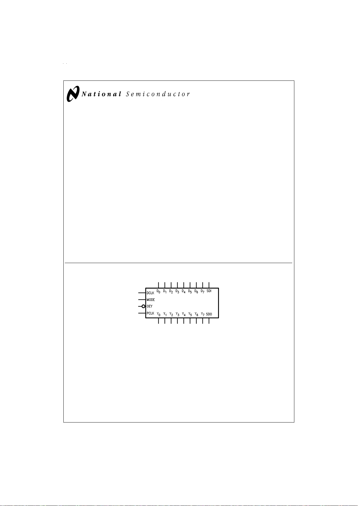
Logic Symbol
TRI-STATE®is a registered trademark of National Semiconductor Corporation.
FACT
™
is a trademark of Fairchild Semiconductor Corporation.
DS100251-3
September 1998
54ACT818 8-Bit Diagnostic Register
© 1998 National Semiconductor Corporation DS100251 www.national.com
Page 2
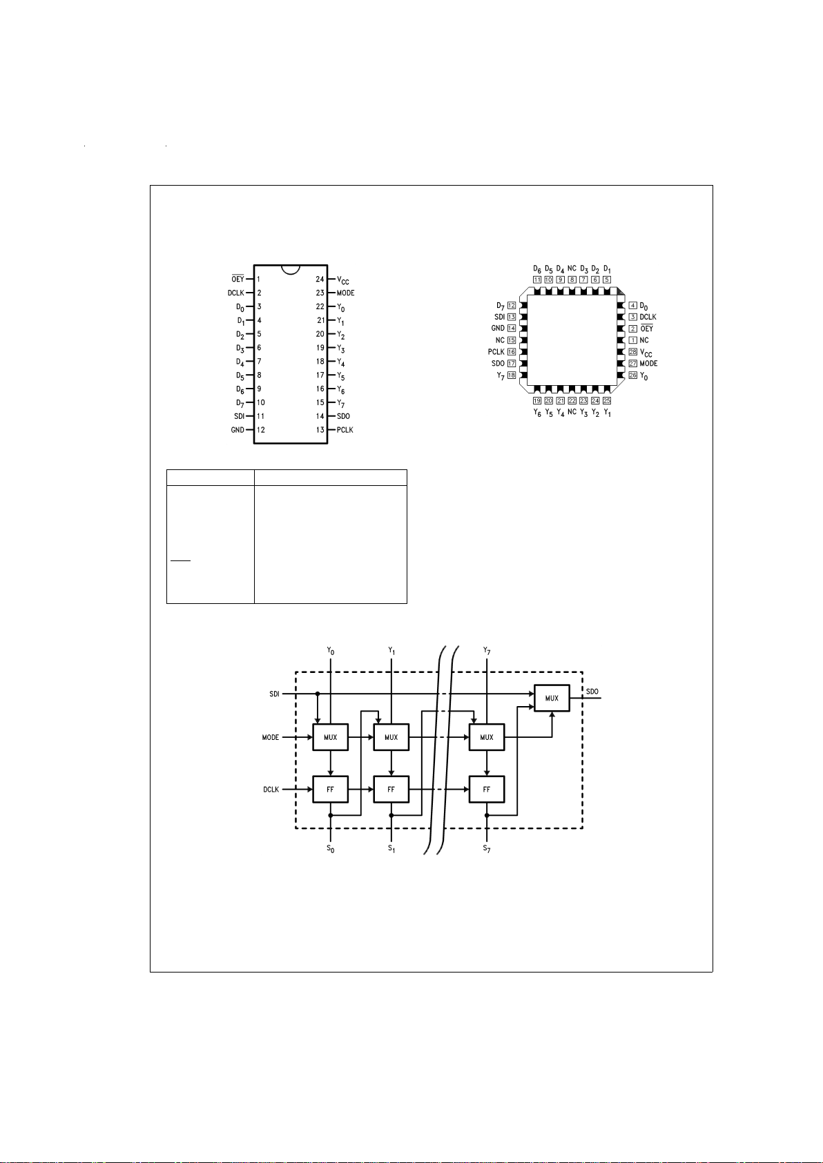
Connection Diagrams
Pin Names Description
D
0–D7
Data Inputs
SDI Serial Data Input
DCLK Diagnostics Clock
MODE Control Input
PCLK Pipeline Register Clock
OEY
Output Enable Input
SDO Serial Data Output
Y
0–Y7
Data Outputs
Diagnostic Register
Pin Assignment
for DIP and Flatpak
DS100251-1
Pin Assignment
for LCC
DS100251-2
DS100251-4
www.national.com 2
Page 3
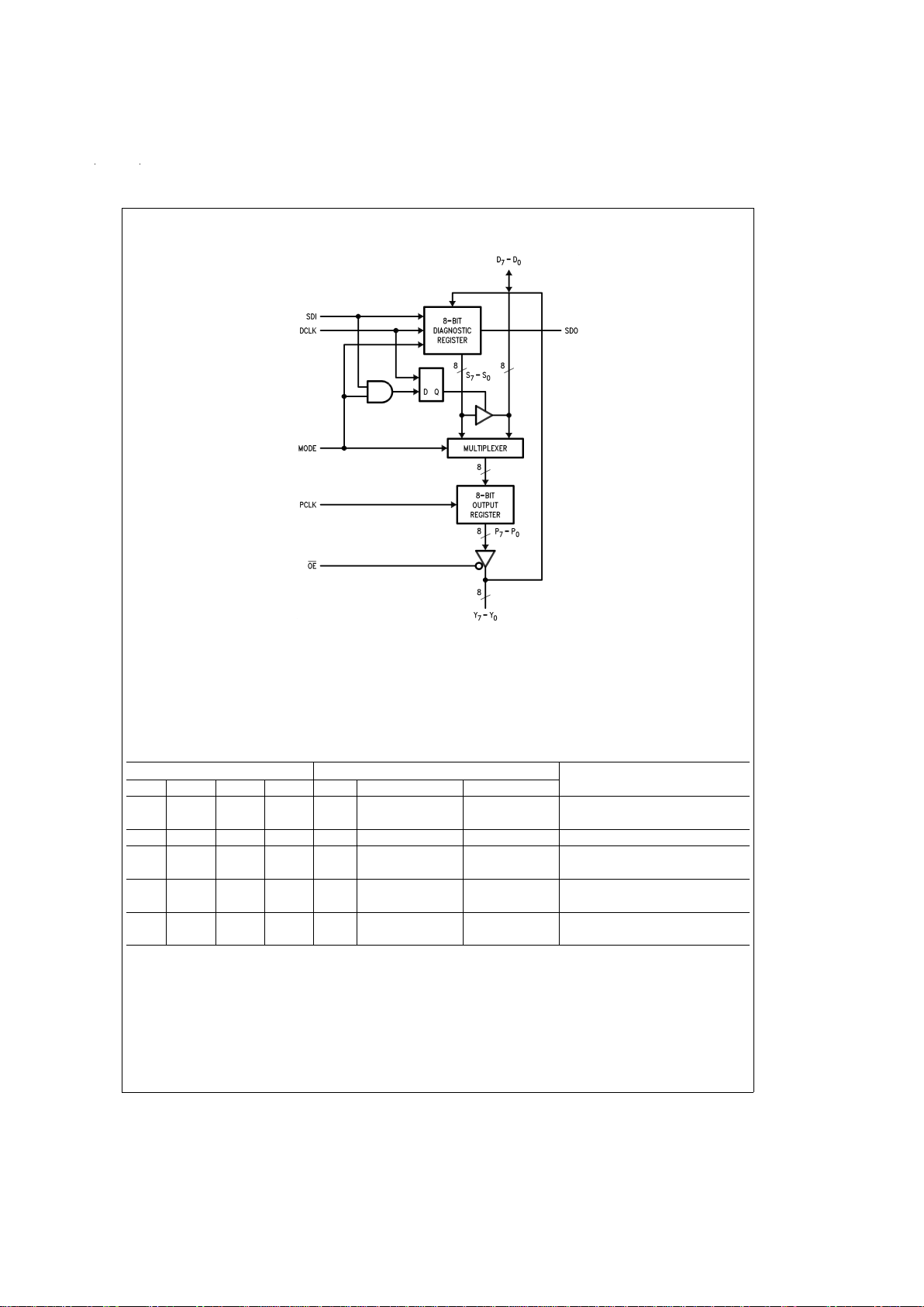
Block Diagram
Functional Description
Data transfers into the diagnostic register occur on the
LOW-to-HIGH transition of DCLK. Mode and SDI determine
what data source will be loaded. The pipeline register is
loaded on the LOW-to-HIGH transition of PCLK. Mode selects whether the data source is the data input or the diag-
nostic register output. Because of the independence of the
clock inputs, data can be shifted in the diagnostic register via
DCLK and loaded into the pipeline register from the data input via PCLK simultaneously, as long as no setup or hold
times are violated. This simultaneous operation is legal.
Function Table
Inputs Outputs Operation
SDI MODE DCLK PCLK SDO Diagnostic Reg. Pipeline Reg.
X L N X S7 SI
<
SI − 1, NA Serial Shift; D7–D0Disabled
SO
<
SD
I
X L X N S7 NA PI<DI Normal Load Pipeline Register
LHN XL SI
<
YI NA Load Diagnostic Register from Y;
DI Disabled
X H X N SDI NA PI
<
SI Load Pipeline Register from
Diagnostic Register
H H N X H Hold NA Hold Diagnostic Register; DI
Enabled
H=HIGH Voltage Level
L=LOW Voltage Level
X=Immaterial
N=LOW-to-HIGH Clock Transition
DS100251-5
www.national.com3
Page 4

Absolute Maximum Ratings (Note 1)
If Military/Aerospace specified devices are required,
please contact the National Semiconductor Sales Office/
Distributors for availability and specifications.
Supply Voltage (V
CC
) −0.5V to +7.0V
DC Input Diode Current (I
IK
)
V
I
=
−0.5V −20 mA
V
I
=
V
CC
+0.5V +20 mA
DC Input Voltage (V
I
) −0.5V to VCC+0.5V
DC Output Diode Current (I
OK
)
V
O
=
−0.5V −20 mA
V
O
=
V
CC
+ 0.5V +20 mA
DC Output Voltage (V
O
) −0.5V to VCC+ 0.5V
DC Output Source
or Sink Current (I
O
)
±
50 mA
DC V
CC
or Ground Current
per Output Pin (I
CC
or I
GND
)
±
50 mA
Storage Temperature (T
STG
) −65˚C to +150˚C
Junction Temperature (T
J
)
CDIP 175˚C
Recommended Operating
Conditions
Supply Voltage (VCC)
’ACT 4.5V to 5.5V
Input Voltage (V
I
) 0VtoV
CC
Output Voltage (VO) 0VtoV
CC
Operating Temperature (TA)
54ACT −55˚C to +125˚C
Minimum Input Edge Rate (∆V/∆t)
’ACT Devices
V
IN
from 0.8V to 2.0V
V
CC
@
4.5V, 5.5V 125 mV/ns
Note 1: Absolute maximum ratings are those values beyond which damage
to the device may occur. The databook specifications should be met, without
exception, to ensure that the system design is reliable over its power supply,
temperature, and output/input loading variables. National does not recommend operation of FACT
™
circuits outside databook specifications.
Note 2: All outputs loaded; thresholds on input associated with output under
test.
DC Characteristics for ’ACT Family Devices
54ACT
Symbol Parameter V
CC
T
A
=
Units Conditions
(V) −55˚C to +125˚C
Guaranteed Limits
V
IH
Minimum High Level 4.5 2.0 V V
OUT
=
0.1V
Input Voltage 5.5 2.0 or V
CC
− 0.1V
V
IL
Maximum Low Level 4.5 0.8 V
OUT
=
0.1V
Input Voltage 5.5 0.8 or V
CC
− 0.1V
I
IN
Maximum Input 5.5
±
1.0 µA V
IN
=
V
CC
Leakage Current
I
OZ
Maximum TRI-STATE 5.5
±
1.0 µA OE=V
IH
Leakage Current V
OUT
=
0V, V
CC
I
CC
Maximum Quiescent 5.5 160 µA V
IN
=
V
CC
or GND
Supply Current
I
CCT
Maximum Additional 5.5 1.6 mA V
IN
=
V
CC
− 2.1V
I
CC
/Input V
CC
=
5.5V
V
OH
Minimum HIGH (Note 2)
V
IN
=
V
IL
or V
IH
Level Output Voltage, 4.5 3.70 V I
OH
=
−24 mA
Y
0–Y7
Outputs 5.5 4.70 V I
OH
=
−24 mA
Minimum HIGH
Level Output Voltage, 4.5 3.70 V I
OH
=
−8 mA
D
0–D7
, SDO Outputs 5.5 4.70 V I
OH
=
−8 mA
V
OL
Maximum LOW (Note 2)
V
IN
=
V
IL
or V
IH
Level Output Voltage, 4.5 0.50 V I
OL
=
24 mA
Y
0–Y7
Outputs 5.5 0.50 V I
OL
=
24 mA
Maximum LOW
Level Output Voltage, 4.5 0.50 V I
OL
=
8mA
D
0–D7
, SDO Outputs 5.5 0.50 V I
OL
=
8mA
www.national.com 4
Page 5

DC Characteristics for ’ACT Family Devices (Continued)
54ACT
Symbol Parameter V
CC
T
A
=
Units Conditions
(V) −55˚C to +125˚C
Guaranteed Limits
I
OLD
Minimum Dynamic V
OLD
=
1.65V Max
Output Current, 5.5 50 mA
Y
0–Y7
Outputs
I
OHD
Minimum Dynamic V
OHD
=
3.85V Min
Output Current, 5.5 −50 mA
Y
0–Y7
Outputs
I
OLD
Minimum Dynamic V
OLD
=
1.65V Max
Output Current, 5.5 32 mA
D
0–D7
, SDO Outputs
(Note 4)
I
OHD
Minimum Dynamic V
OHD
=
3.85V Min
Output Current, 5.5 −32 mA
D
0–D7
, SDO Outputs
(Note 4)
Note 3: Maximum test duration 2.0 ms, one output loaded at a time.
Note 4: Test load 50 pF, 500Ω to ground.
Note 5: I
CC
for 54ACT@25˚C is identical to 74ACT@25˚C.
AC Electrical Characteristics
54ACT
V
CC
T
A
=
−55˚C Fig.
Symbol Parameter (V) to +125˚C Units No.
(Note 6) C
L
=
50 pF
Min Max
t
PHL
Propagation Delay 5.0 2.5 10.0 ns
PCLK to Y
t
PLH
Propagation Delay 5.0 2.5 10.0 ns
PCLK to Y
t
PHL
Propagation Delay 5.0 3.5 12.0 ns
MODE to SDO
t
PLH
Propagation Delay 5.0 3.5 13.5 ns
MODE to SDO
t
PHL
Propagation Delay 5.0 3.0 11.5 ns
SDI to SDO
t
PLH
Propagation Delay 5.0 3.0 12.0 ns
SDI to SDO
t
PHL
Propagation Delay 5.0 3.5 14.0 ns
DCLK to SDO
t
PLH
Propagation Delay 5.0 3.5 15.5 ns
DCLK to SDO
t
PZL
Output Enable Time 5.0 2.5 12.0 ns
OEY to Y
n
t
PLZ
Output Disable Time 5.0 1.5 10.0 ns
OEY to Y
n
t
PZL
Output Enable Time 5.0 3.0 14.0 ns
DCLK to D
n
www.national.com5
Page 6

AC Electrical Characteristics (Continued)
54ACT
V
CC
T
A
=
−55˚C Fig.
Symbol Parameter (V) to +125˚C Units No.
(Note 6) C
L
=
50 pF
Min Max
t
PLZ
Output Disable Time 5.0 1.5 12.0 ns
DCLK to D
n
t
PZH
Output Enable Time 5.0 2.5 11.0 ns
OEY to Y
n
t
PHZ
Output Disable Time 5.0 2.0 12.0 ns
OEY to Y
n
t
PZH
Output Enable Time 5.0 3.0 13.5 ns
DCLK to D
n
t
PHZ
Output Disable Time 5.0 2.0 13.5 ns
DCLK to D
n
Note 6: Voltage Range 5.0 is 5.0V±0.5V.
AC Operating Requirements
54ACT
V
CC
T
A
=
−55˚C Fig.
Symbol Parameter (V) to +125˚C Units No.
(Note 8) C
L
=
50 pF
Guaranteed Minimum
t
s
Setup Time 5.0 6.0 ns
D to PCLK
t
h
Hold Time 5.0 1.0 ns
D to PCLK
t
s
Setup Time 5.0 6.0 ns
MODE to PCLK
t
h
Hold Time 5.0 0.0 ns
MODE to PCLK
t
s
Setup Time 5.0 2.5 ns
Y to DCLK
t
h
Hold Time 5.0 1.5 ns
Y to DCLK
t
s
Setup Time 5.0 4.5 ns
MODE to DCLK
t
h
Hold Time 5.0 1.0 ns
MODE to DCLK
t
s
Setup Time 5.0 4.5 ns
SDI to DCLK
t
h
Hold Time 5.0 1.0 ns
SDI to DCLK
t
s
Setup Time 5.0 11.5 ns
DCLK to PCLK
t
s
Setup Time 5.0 12.5 ns
PCLK to DCLK
t
w
Pulse Width 5.0 3.5 ns
www.national.com 6
Page 7

AC Operating Requirements (Continued)
54ACT
V
CC
T
A
=
−55˚C Fig.
Symbol Parameter (V) to +125˚C Units No.
(Note 8) C
L
=
50 pF
Guaranteed Minimum
PCLK HIGH or
LOW
t
w
Pulse Width 5.0 3.0 ns
DCLK HIGH or
LOW
Note 7: Test load 50 pF, 500Ω to ground.
Note 8: Voltage range 5.0 is 5.0V
±
0.5V.
Capacitance
Symbol Parameter Typ Units Conditions
C
IN
Input Capacitance 4.5 pF V
CC
=
OPEN
C
PD
Power Dissipation 20 pF V
CC
=
5.0V
Capacitance
www.national.com7
Page 8

8
Page 9

Physical Dimensions inches (millimeters) unless otherwise noted
28 Terminal Ceramic Leadless Chip Carrier (L)
NS Package Number E28A
24 Lead Slim (0.300" wide) Ceramic Dual-in-Line Package (D)
NS Package Number J24F
www.national.com9
Page 10

Physical Dimensions inches (millimeters) unless otherwise noted (Continued)
LIFE SUPPORT POLICY
NATIONAL’S PRODUCTS ARE NOT AUTHORIZED FOR USE AS CRITICAL COMPONENTS IN LIFE SUPPORT DEVICES OR SYSTEMS WITHOUT THE EXPRESS WRITTEN APPROVAL OF THE PRESIDENT OF NATIONAL SEMICONDUCTOR CORPORATION. As used herein:
1. Life support devices or systems are devices or systems which, (a) are intended for surgical implant into
the body, or (b) support or sustain life, and whose failure to perform when properly used in accordance
with instructions for use provided in the labeling, can
be reasonably expected to result in a significant injury
to the user.
2. A critical component in any component of a life support
device or system whose failure to perform can be reasonably expected to cause the failure of the life support
device or system, or to affect its safety or effectiveness.
National Semiconductor
Corporation
Americas
Tel: 1-800-272-9959
Fax: 1-800-737-7018
Email: support@nsc.com
www.national.com
National Semiconductor
Europe
Fax: +49 (0) 1 80-530 85 86
Email: europe.support@nsc.com
Deutsch Tel: +49 (0) 1 80-530 85 85
English Tel: +49 (0) 1 80-532 78 32
Français Tel: +49 (0) 1 80-532 93 58
Italiano Tel: +49 (0) 1 80-534 16 80
National Semiconductor
Asia Pacific Customer
Response Group
Tel: 65-2544466
Fax: 65-2504466
Email: sea.support@nsc.com
National Semiconductor
Japan Ltd.
Tel: 81-3-5620-6175
Fax: 81-3-5620-6179
24 Lead Ceramic Cerpack
NS Package Number W24C
54ACT818 8-Bit Diagnostic Register
National does not assume any responsibility for use of any circuitry described, no circuit patent licenses are implied and National reserves the right at any time without notice to change said circuitry and specifications.
 Loading...