

Page 1

54ACTQ32
Quiet Series Quad 2-Input OR Gate
General Description
The ’ACTQ32 contains four, 2-input OR gates and utilizes
NSC Quiet Series technology to guarantee quiet output
switching and improved dynamic threshold performance.
FACT Quiet Series
™
features GTO™output control and undershoot corrector in addition to a split ground bus for superior ACMOS performance.
Features
n ICCreduced by 50
%
n Guaranteed simultaneous switching noise level and
dynamic threshold performance
n Improved latch-up immunity
n Outputs source/sink 24 mA
n ’ACTQ32 has TTL-compatible inputs
n Standard Microcircuit Drawing (SMD) 5962-8973601
Logic Symbol
Connection Diagrams
Pin Names Description
A
n,Bn
Inputs
O
n
Outputs
GTO™is a trademark of National Semiconductor Corporation.
FACT
™
and FACT Quiet Series™are trademarks of Fairchild Semiconductor Corporation.
IEEE/IEC
DS100984-1
Pin Assignment for DIP and Flatpak
DS100984-3
Pin Assignment for LCC
DS100984-2
September 1998
54ACTQ32 Quiet Series Quad 2-Input OR Gate
© 1998 National Semiconductor Corporation DS100984 www.national.com
Page 2

Absolute Maximum Ratings (Note 1)
If Military/Aerospace specified devices are required,
please contact the National Semiconductor Sales Office/
Distributors for availability and specifications.
Supply Voltage (V
CC
) −0.5V to +7.0V
DC Input Diode Current (I
IK
)
V
I
=
−0.5V −20 mA
V
I
=
V
CC
+ 0.5V +20 mA
DC Input Voltage (V
I
) −0.5V to VCC+ 0.5V
DC Output Diode Current (I
OK
)
V
O
=
−0.5V −20 mA
V
O
=
V
CC
+ 0.5V +20 mA
DC Output Voltage (V
O
) −0.5V to VCC+ 0.5V
DC Output Source
or Sink Current (I
O
)
±
50 mA
DC V
CC
or Ground Current
per Output Pin (I
CC
or I
GND
)
±
50 mA
Storage Temperature (T
STG
) −65˚C to +150˚C
Junction Temperature (T
J
)
CDIP 175˚C
Recommended Operating
Conditions
Supply Voltage (VCC)
’ACTQ 4.5V to 5.5V
Input Voltage (V
I
) 0VtoV
CC
Output Voltage (VO) 0VtoV
CC
Operating Temperature (TA)
54ACTQ −55˚C to +125˚C
Minimum Input Edge Rate (∆V/∆t)
’ACTQ Devices
V
IN
from 0.8V to 2.0V
V
CC
@
4.5V, 5.5V 125 mV/ns
Note 1: Absolute maximum ratings are those values beyond which damage
to the device may occur. The databook specifications should be met, without
exception, to ensure that the system design is reliable over its power supply,
temperature, and output/input loading variables. National does not recommend operation of FACT
™
circuits outside databook specifications.
DC Characteristics for ’ACTQ Family Devices
54ACTQ
Symbol Parameter V
CC
T
A
=
Units Conditions
(V) −55˚C to +125˚C
Guaranteed Limits
V
IH
Minimum High Level 4.5 2.0 V V
OUT
=
0.1V
Input Voltage 5.5 2.0 or V
CC
− 0.1V
V
IL
Maximum Low Level 4.5 0.8 V V
OUT
=
0.1V
Input Voltage 5.5 0.8 or V
CC
− 0.1V
V
OH
Minimum High Level 4.5 4.4 V I
OUT
=
−50 µA
Output Voltage 5.5 5.4
(Note 2)
V
IN
=
V
IL
or V
IH
4.5 3.70 V IOH= −24 mA
5.5 4.70 I
OH
= −24 mA
V
OL
Maximum Low Level 4.5 0.1 V I
OUT
=
50 µA
Output Voltage 5.5 0.1
(Note 2)
V
IN
=
V
IL
or V
IH
4.5 0.50 V IOL=24mA
5.5 0.50 I
OL
=24mA
I
IN
Maximum Input 5.5
±
1.0 µA V
I
=
V
CC
, GND
Leakage Current
I
CCT
Maximum 5.5 1.6 mA V
I
=
V
CC
− 2.1V
I
CC
/Input
I
OLD
Minimum Dynamic 5.5 50 mA V
OLD
=
1.65V Max
I
OHD
Output Current (Note 3) 5.5 −50 mA V
OHD
=
3.85V Min
I
CC
Maximum Quiescent 5.5 80.0 µA V
IN
=
V
CC
Supply Current or GND (Note 3)
Note 2: All outputs loaded; thresholds on input associated with output under test.
Note 3: Maximum test duration 2.0 ms, one output loaded at a time.
www.national.com 2
Page 3
AC Electrical Characteristics
54ACTQ
V
CC
T
A
=
−55˚C Fig.
Symbol Parameter (V) to +125˚C Units No.
(Note 4) C
L
=
50 pF
Min Max
t
PLH
Propagation Delay 5.0 1.5 7.5 ns
t
PHL
Propagation Delay 5.0 1.5 7.5 ns
Note 4: Voltage Range 5.0 is 5.0V±0.5V
Capacitance
Symbol Parameter Max Units Conditions
C
IN
Input Capacitance 10.0 pF V
CC
=
OPEN
C
PD
Power Dissipation 72.0 pF V
CC
=
5.0V
Capacitance
www.national.com3
Page 4

4
Page 5
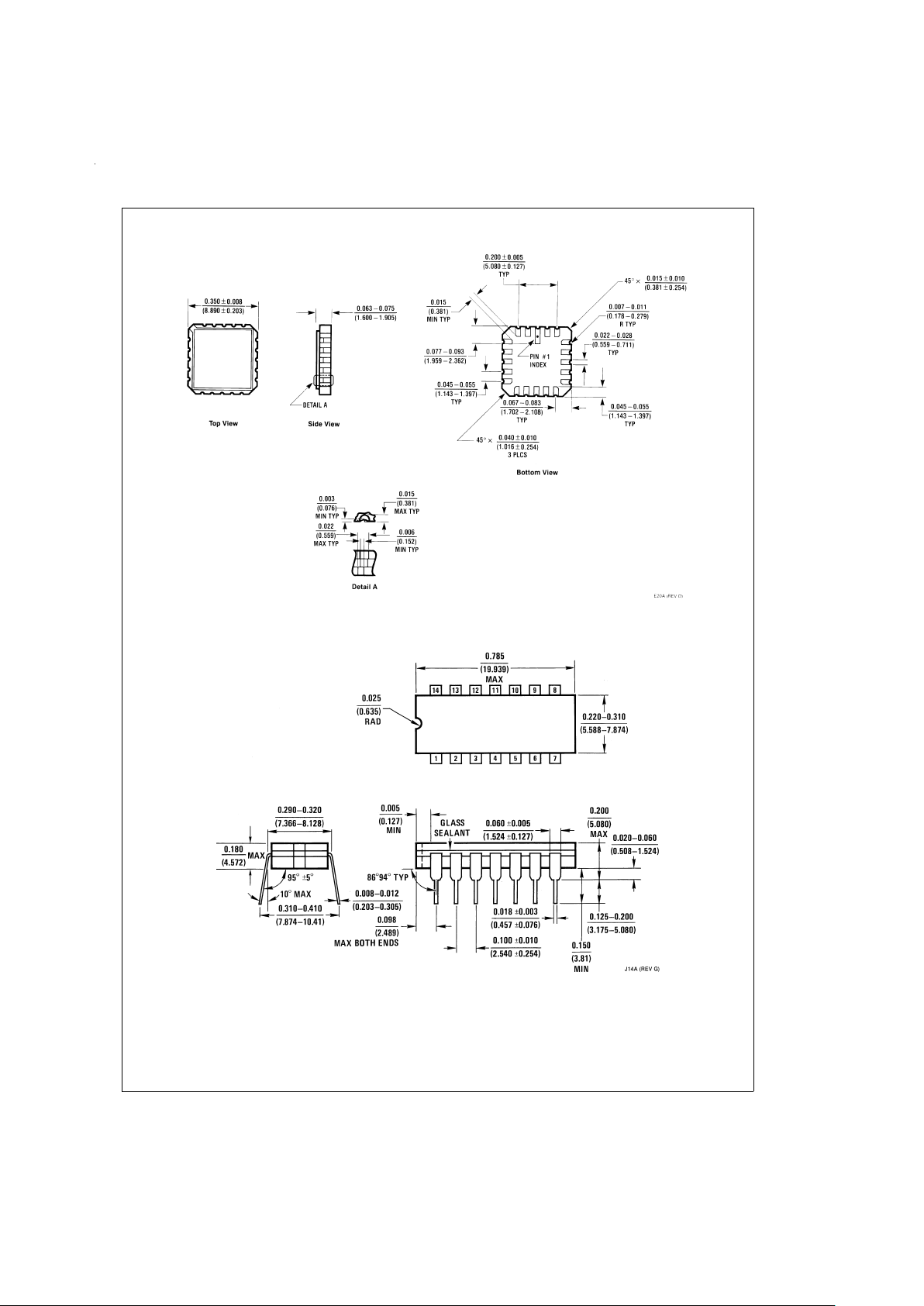
Physical Dimensions inches (millimeters) unless otherwise noted
20 Terminal Ceramic Leadless Chip Carrier (L)
NS Package Number E20A
14-Lead Ceramic Dual-In-Line Package (D)
NS Package Number J14A
www.national.com5
Page 6
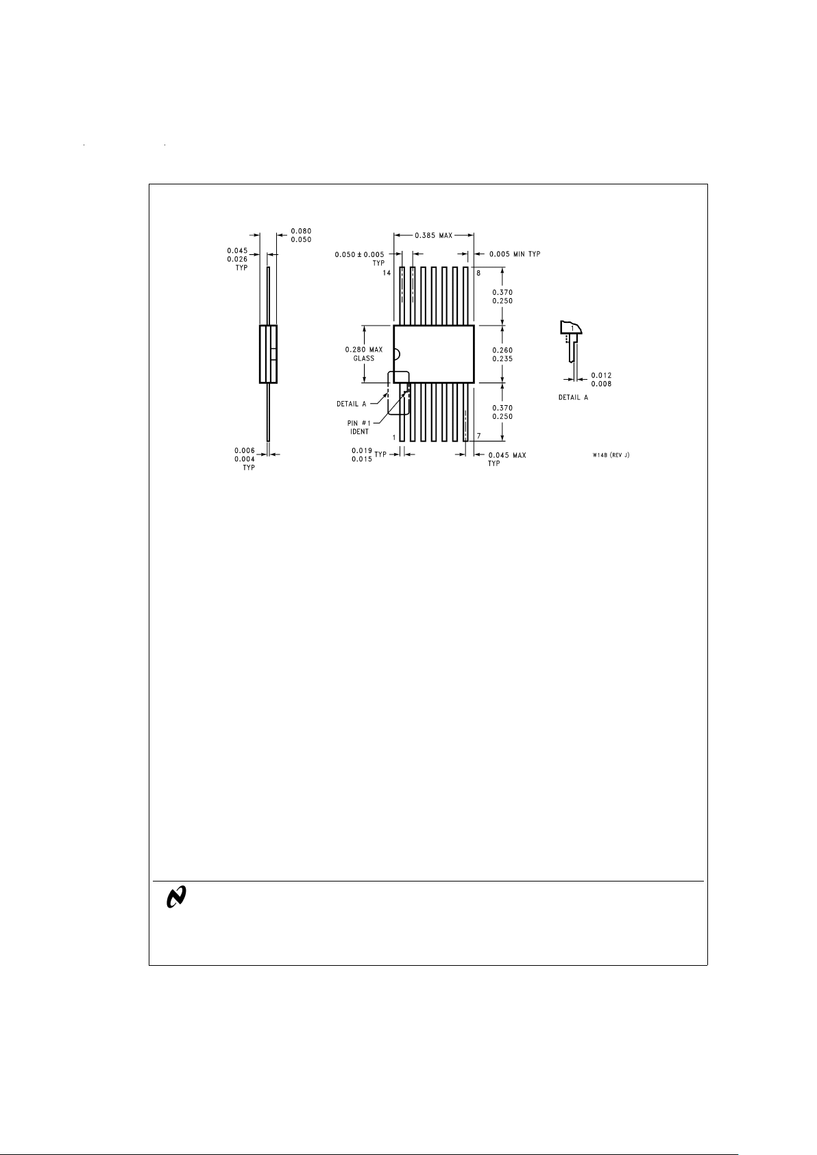
Physical Dimensions inches (millimeters) unless otherwise noted (Continued)
LIFE SUPPORT POLICY
NATIONAL’S PRODUCTS ARE NOT AUTHORIZED FOR USE AS CRITICAL COMPONENTS IN LIFE SUPPORT DEVICES OR SYSTEMS WITHOUT THE EXPRESS WRITTEN APPROVAL OF THE PRESIDENT OF NATIONAL SEMICONDUCTOR CORPORATION. As used herein:
1. Life support devices or systems are devices or systems which, (a) are intended for surgical implant into
the body, or (b) supportorsustainlife, and whose failure to perform when properly used in accordance
with instructions for use provided in the labeling, can
be reasonably expected to resultina significant injury
to the user.
2. A critical component in any component of a life support
device or system whose failure to perform can be reasonably expected to causethe failure of thelife support
device or system, or toaffectits safety or effectiveness.
National Semiconductor
Corporation
Americas
Tel: 1-800-272-9959
Fax: 1-800-737-7018
Email: [email protected]
www.national.com
National Semiconductor
Europe
Fax: +49 (0) 1 80-530 85 86
Email: [email protected]
Deutsch Tel: +49 (0) 1 80-530 85 85
English Tel: +49 (0) 1 80-532 78 32
Français Tel: +49 (0) 1 80-532 93 58
Italiano Tel: +49 (0) 1 80-534 16 80
National Semiconductor
Asia Pacific Customer
Response Group
Tel: 65-2544466
Fax: 65-2504466
Email: [email protected]
National Semiconductor
Japan Ltd.
Tel: 81-3-5620-6175
Fax: 81-3-5620-6179
14-Lead Ceramic Flatpak (F)
NS Package Number W14B
54ACTQ32 Quiet Series Quad 2-Input OR Gate
National does not assume any responsibility for use of any circuitry described, no circuit patent licenses are implied and National reserves the right at anytime without notice to change said circuitry and specifications.
 Loading...