

Page 1
TL7702A, TL7705A, TL7709A, TL7712A, TL7715A
SUPPLY-VOLTAGE SUPERVISORS
SLVS028E – APRIL 1983 – REVISED JULY 1999
1
POST OFFICE BOX 655303 • DALLAS, TEXAS 75265
D
Power-On Reset Generator
D
Automatic Reset Generation After Voltage
Drop
D
Wide Supply-Voltage Range
D
Precision V oltage Sensor
D
T emperature-Compensated Voltage
Reference
D
True and Complement Reset Outputs
D
Externally Adjustable Pulse Duration
description
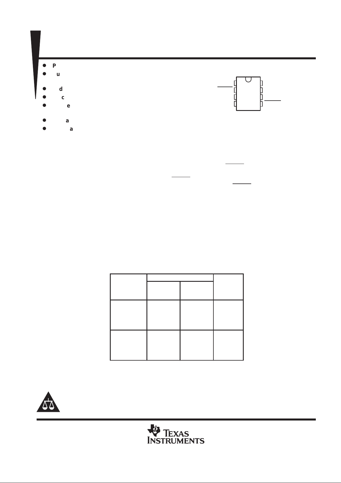
The TL77xxA family of integrated-circuit supply-voltage supervisors is specifically designed for use as reset
controllers in microcomputer and microprocessor systems. The supply-voltage supervisor monitors the supply
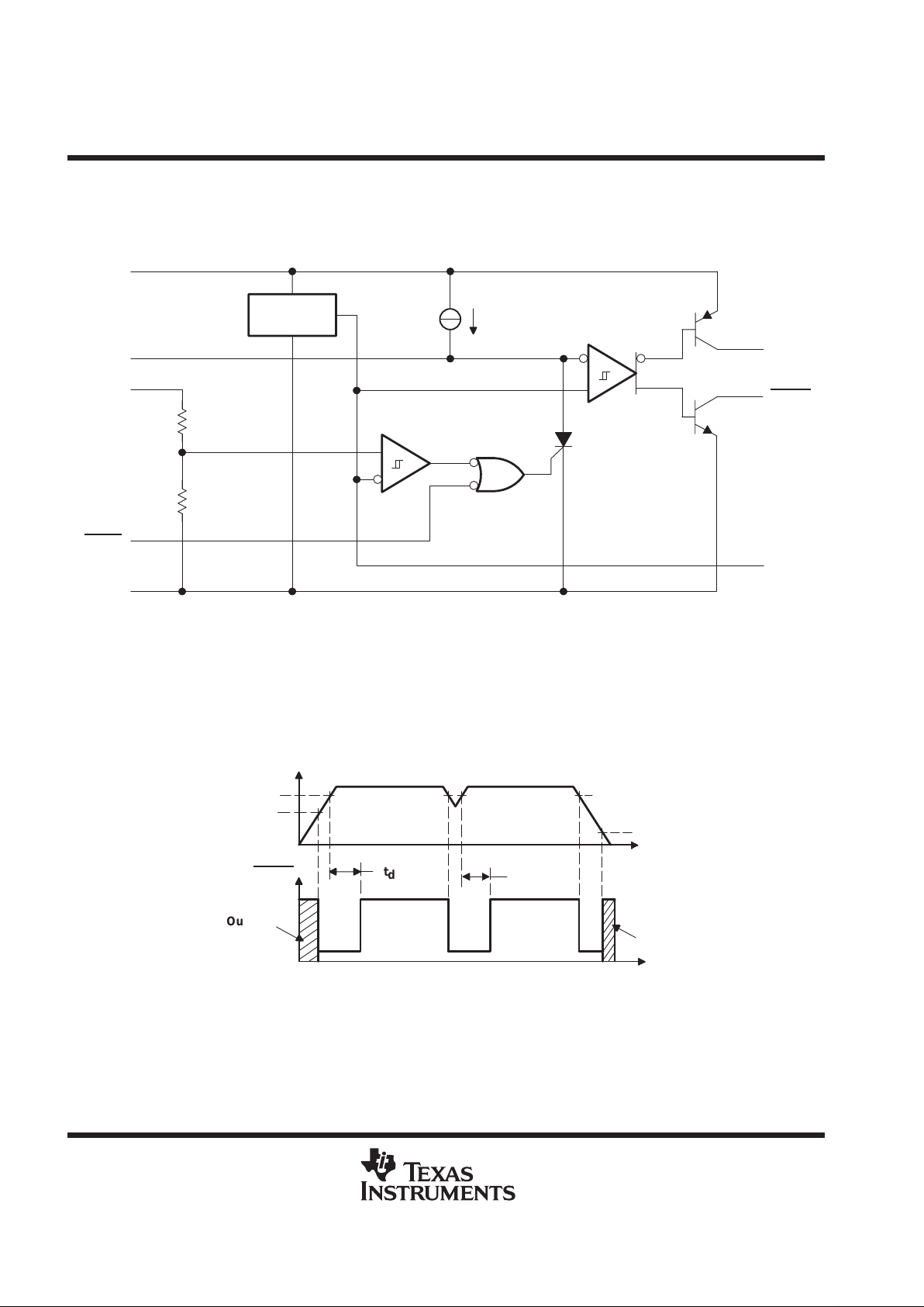
for undervoltage conditions at the SENSE input. During power up, the RESET output becomes active (low)
when V
CC
attains a value approaching 3.6 V . At this point (assuming that SENSE is above V
IT+
), the delay timer
function activates a time delay , after which outputs RESET and RESET go inactive (high and low, respectively).
When an undervoltage condition occurs during normal operation, outputs RESET and RESET go active. To
ensure that a complete reset occurs, the reset outputs remain active for a time delay after the voltage at the
SENSE input exceeds the positive-going threshold value. The time delay is determined by the value of the
external capacitor C
T
: td = 1.3 × 10⁴ × CT, where CT is in farads (F) and td is in seconds (s).
During power down (assuming that SENSE is below V
IT–
), the outputs remain active until the VCC falls below
a maximum of 2 V. After this, the outputs are undefined.
An external capacitor (typically 0.1 µF for the TL77xxAC and TL77xxAI) must be connected to REF to reduce
the influence of fast transients in the supply voltage.
The TL77xxAC series is characterized for operation from 0°C to 70°C. The TL77xxAI series is characterized
for operation from –40°C to 85°C.
AVAILABLE OPTIONS
PACKAGED DEVICES
T
A
SMALL
OUTLINE
(D)
PLASTIC
DIP
(P)
CHIP
FORM
(Y)
0°C to 70°C
TL7702ACD
TL7705ACD
TL7709ACD
TL7712ACD
TL7715ACD
TL7702ACP
TL7705ACP
TL7709ACP
TL7712ACP
TL7715ACP
TL7702ACY
TL7705ACY
TL7709ACY
TL7712ACY
TL7715ACY
–40°C to 85°C
TL7702AID
TL7705AID
TL7709AID
TL7712AID
TL7715AID
TL7702AIP
TL7705AIP
TL7709AIP
TL7712AIP
TL7715AIP
—
—
—
—
—
The D package is available taped and reeled. Add the suffix R to the
device type (e.g., TL7702ACDR). Chip forms are tested at 25°C.
Copyright 1999, Texas Instruments Incorporated
PRODUCTION DATA information is current as of publication date.
Products conform to specifications per the terms of Texas Instruments
standard warranty. Production processing does not necessarily include
testing of all parameters.
Please be aware that an important notice concerning availability, standard warranty, and use in critical applications of
Texas Instruments semiconductor products and disclaimers thereto appears at the end of this data sheet.
1
2
3
4
8
7
6
5
REF
RESIN
CT
GND
V
CC
SENSE
RESET
RESET
D OR P PACKAGE
(TOP VIEW)
Page 2
TL7702A, TL7705A, TL7709A, TL7712A, TL7715A
SUPPLY-VOLTAGE SUPERVISORS
SLVS028E – APRIL 1983 – REVISED JULY 1999
2
POST OFFICE BOX 655303 • DALLAS, TEXAS 75265
functional block diagram
The functional block diagram is shown for illustrative purposes only; the actual circuit includes a trimming
network to adjust the reference voltage and sense-comparator trip point.
RESIN
≈100 µA
R1
(see Note A)
6
5
1
Reference
Voltage
SENSE
GND
8
3
7
2
4
V
CC
CT
RESET
RESET
REF
R2
(see Note A)
NOTES: A. TL7702A: R1 = 0 Ω, R2 = open
TL7705A: R1 = 7.8 kΩ, R2 = 10 kΩ
TL7709A: R1 = 19.7 kΩ, R2 = 10 kΩ
TL7712A: R1 = 32.7 kΩ, R2 = 10 kΩ
TL7715A: R1 = 43.4 kΩ, R2 = 10 kΩ
B. Resistor values shown are nominal.
timing diagram
Output
Undefined
RESET
t
d
Output
Undefined
VCC and SENSE
t
d
Threshold Voltage
VCC ≈ 3.6 V
VCC ≈ 2 V
Page 3
TL7702A, TL7705A, TL7709A, TL7712A, TL7715A
SUPPLY-VOLTAGE SUPERVISORS
SLVS028E – APRIL 1983 – REVISED JULY 1999
3
POST OFFICE BOX 655303 • DALLAS, TEXAS 75265
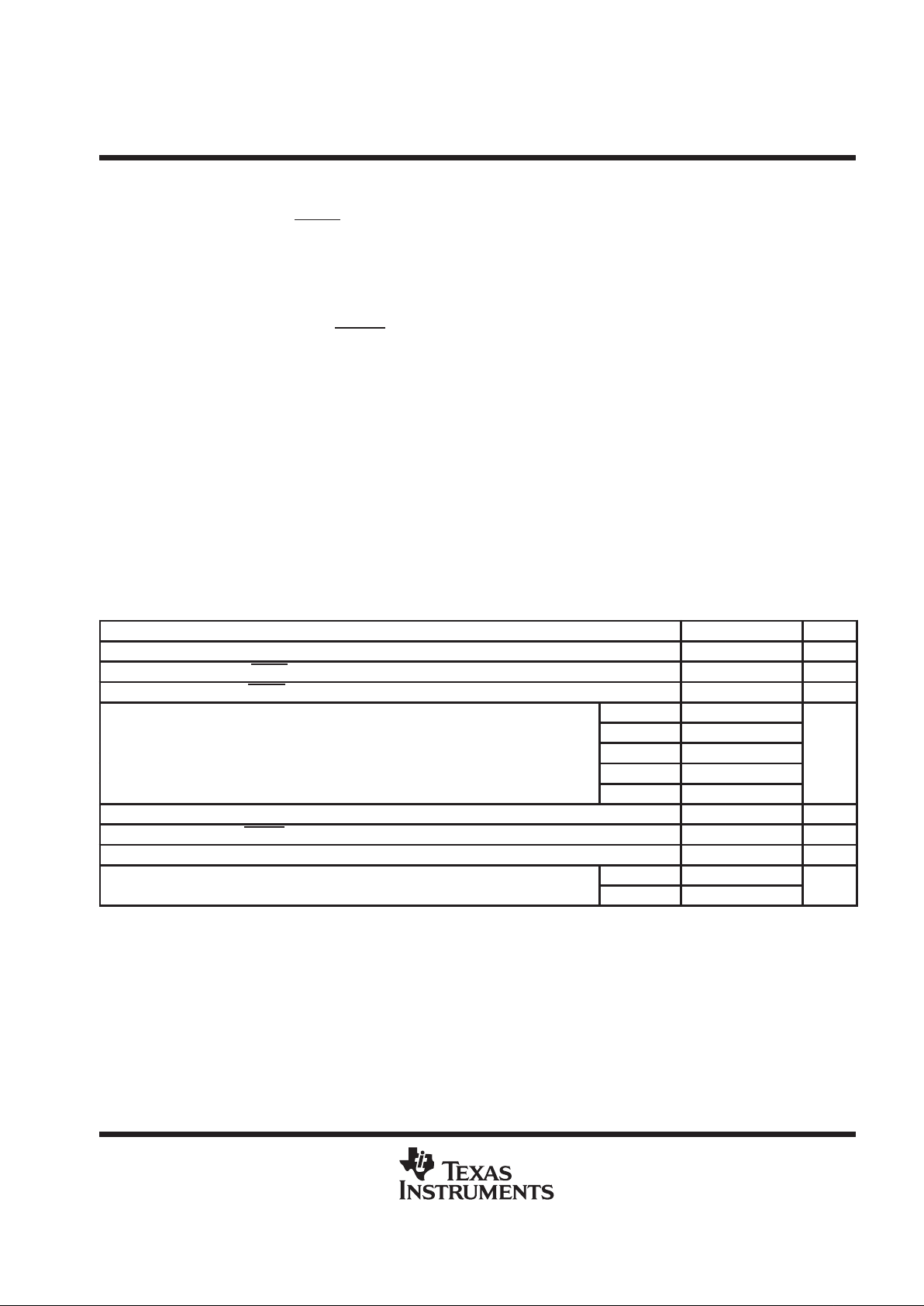
absolute maximum ratings over operating free-air temperature (unless otherwise noted)
†
Supply voltage, VCC (see Note 1) 20 V. . . . . . . . . . . . . . . . . . . . . . . . . . . . . . . . . . . . . . . . . . . . . . . . . . . . . . . . . . . .
Input voltage range, VI, RESIN –0.3 V to 20 V. . . . . . . . . . . . . . . . . . . . . . . . . . . . . . . . . . . . . . . . . . . . . . . . . . . . .
Input voltage range, VI, SENSE:TL7702A (see Note 2) –0.3 V to 6 V. . . . . . . . . . . . . . . . . . . . . . . . . . . . . . . . .
TL7705A –0.3 V to 20 V. . . . . . . . . . . . . . . . . . . . . . . . . . . . . . . . . . . . . . . . . . .
TL7709A –0.3 V to 20 V. . . . . . . . . . . . . . . . . . . . . . . . . . . . . . . . . . . . . . . . . . . .
TL7712A, TL7715A –0.3 V to 20 V. . . . . . . . . . . . . . . . . . . . . . . . . . . . . . . . . . .
High-level output current, I
OH
, RESET –30 mA. . . . . . . . . . . . . . . . . . . . . . . . . . . . . . . . . . . . . . . . . . . . . . . . . . . . .
Low-level output current, IOL, RESET 30 mA. . . . . . . . . . . . . . . . . . . . . . . . . . . . . . . . . . . . . . . . . . . . . . . . . . . . . .
Package thermal impedance, θJA (see Notes 3 and 4): D package 97°C/W. . . . . . . . . . . . . . . . . . . . . . . . . . . .
P package 127°C/W. . . . . . . . . . . . . . . . . . . . . . . . . . .
Lead temperature 1,6 mm (1/16 inch) from case for 10 seconds: D or P package 260°C. . . . . . . . . . . . . . . . .
Storage temperature range, T
stg
–65°C to 150°C. . . . . . . . . . . . . . . . . . . . . . . . . . . . . . . . . . . . . . . . . . . . . . . . . .
†
Stresses beyond those listed under “absolute maximum ratings” may cause permanent damage to the device. These are stress ratings only, and
functional operation of the device at these or any other conditions beyond those indicated under “recommended operating conditions” is not
implied. Exposure to absolute-maximum-rated conditions for extended periods may affect device reliability.
NOTES: 1. All voltage values are with respect to the network ground terminal.
2. For proper operation of the TL7702A, the voltage applied to the SENSE terminal should not exceed VCC – 1 V or 6 V , whichever
is less.
3. Maximum power dissipation is a function of TJ(max),
θ
JA
, and TA. The maximum allowable power dissipation at any allowable
ambient temperature is PD = (TJ(max) – TA)/
θ
JA
. Operating at the absolute maximum TJ of 150°C can impact reliability.
4. The package thermal impedance is calculated in accordance with JESD 51, except for through-hole packages, which use a trace
length of zero.
recommended operating conditions
MIN MAX UNIT
Supply voltage, V
CC
3.5 18 V
High-level input voltage at RESIN, V
IH
2 V
Low-level input voltage at RESIN, V
IL
0.6 V
TL7702A 0 See Note 2
TL7705A 0 10
Input voltage, SENSE, V
I
TL7709A 0 15
V
TL7712A 0 20
TL7715A 0 20
High-level output current, RESET, I
OH
–16 mA
Low-level output current, RESET, I
OL
16 mA
Timing capacitor , C
T
10 µF
p
p
TL77xxAC 0 70
°
Operating free-air temperature range, T
A
TL77xxAI –40 85
°C
NOTE 2: For proper operation of the TL7702A, the voltage applied to the SENSE terminal should not exceed VCC – 1 V or 6 V , whichever is less.
Page 4
TL7702A, TL7705A, TL7709A, TL7712A, TL7715A
SUPPLY-VOLTAGE SUPERVISORS
SLVS028E – APRIL 1983 – REVISED JULY 1999
4
POST OFFICE BOX 655303 • DALLAS, TEXAS 75265
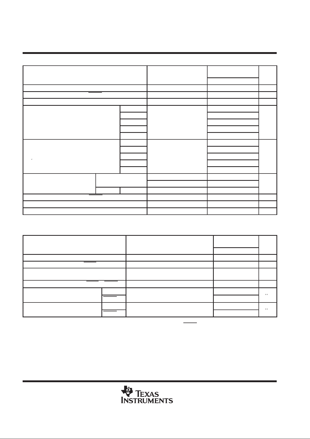
electrical characteristics over recommended operating conditions (unless otherwise noted)
PARAMETER
TEST CONDITIONS
†
TL77xxAC
TL77xxAI
UNIT
MIN TYP MAX
V
OH
High-level output voltage, RESET IOH = –16 mA VCC–1.5 V
V
OL
Low-level output voltage, RESET IOL = 16 mA 0.4 V
V
ref
Reference voltage TA = 25°C 2.48 2.53 2.58 V
TL7702A 2.48 2.53 2.58
TL7705A 4.5 4.55 4.6
V
IT–
Negative-going input threshold voltage,
TL7709A
TA = 25°C
7.5 7.6 7.7
V
SENSE
TL7712A 10.6 10.8 11
TL7715A 13.2 13.5 13.8
TL7702A 10
TL7705A 15
V
hys
Hysteresis, SENSE (V
IT+
– V
IT–
)
TL7709A
TA = 25°C
20
mV
y
TL7712A 35
TL7715A 45
VI = 2.4 V to V
CC
20
I
I
Input current
RESIN
VI = 0.4 V –100
µA
SENSE TL7702A V
ref
< VI < VCC – 1.5 V 0.5 2
I
OH
High-level output current, RESET VO = 18 V 50 µA
I
OL
Low-level output current, RESET VO = 0 –50 µA
I
CC
Supply current All inputs and outputs open 1.8 3 mA
†
All electrical characteristics are measured with 0.1-µF capacitors connected at REF, CT , and VCC to GND.
switching characteristics over recommended operating conditions (unless otherwise noted)
PARAMETER
TEST CONDITIONS
‡
TL77xxAC
TL77xxAI
UNIT
MIN TYP MAX
Output pulse duration CT = 0.1 µF 0.65 1.2 2.6 µs
Input pulse duration at RESIN 0.4 µs
t
w(S)
Pulse duration
at SENSE input to switch outputs
VIH = V
IT–
+200 mV , VIL = V
IT–
–200 mV 2 µs
t
pd
Propagation delay time, RESIN to RESET VCC = 5 V 1 µs
RESET
0.2
trRise time
RESET
V
CC
= 5 V,
See Note 5
3.5
µ
s
RESET
3.5
tfFall time
RESET
V
CC
= 5 V,
See Note 5
0.2
µ
s
‡
All switching characteristics are measured with 0.1-µF capacitors connected at REF and VCC to GND.
NOTE 5: The rise and fall times are measured with a 4.7-kΩ load resistor at RESET and RESET
.
Page 5
TL7702A, TL7705A, TL7709A, TL7712A, TL7715A
SUPPLY-VOLTAGE SUPERVISORS
SLVS028E – APRIL 1983 – REVISED JULY 1999
5
POST OFFICE BOX 655303 • DALLAS, TEXAS 75265
electrical characteristics over recommended operating conditions, TA = 25°C (unless otherwise
noted)
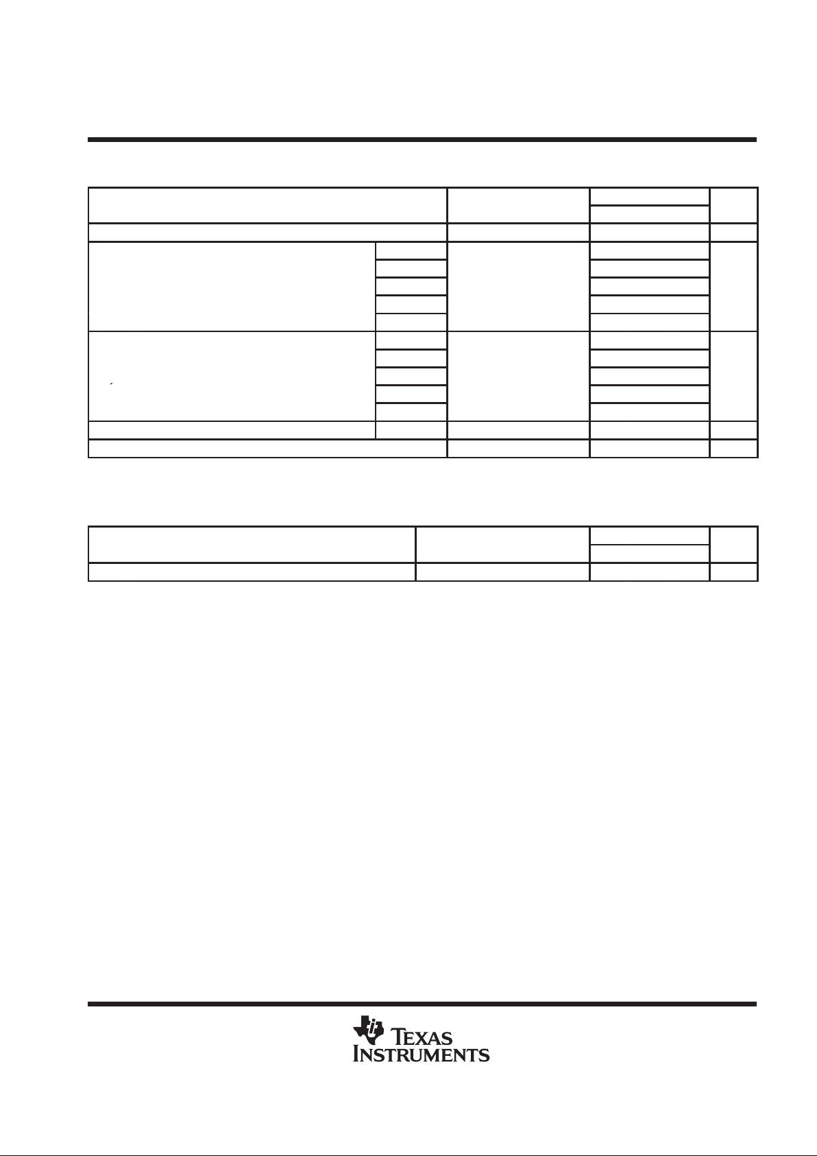
TL77xxAY
PARAMETER
TEST CONDITIONS
†
MIN TYP MAX
UNIT
V
ref
Reference voltage 2.53 V
TL7702A 2.53
TL7705A 4.55
V
IT–
Negative-going input threshold voltage, SENSE
TL7709A
7.6
V
TL7712A 10.8
TL7715A 13.5
TL7702A 10
TL7705A 15
V
h
y
s
Hysteresis, SENSE (V
IT+
– V
IT–
)
TL7709A
20
mV
y
TL7712A 35
TL7715A 45
I
I
Input current, SENSE TL7702A V
ref
< VI < VCC – 1.5 V 0.5 µA
I
CC
Supply current All inputs and outputs open 1.8 mA
†
All electrical characteristics are measured with 0.1-µF capacitors connected at REF, CT , and VCC to GND.
switching characteristics over recommended operating conditions, TA = 25°C (unless otherwise
noted)
TL77xxAY
PARAMETER
TEST CONDITIONS
‡
MIN TYP MAX
UNIT
t
d
Output pulse time delay CT = 0.1 µF 1.2 µs
‡
All switching characteristics are measured with 0.1-µF capacitors connected at REF and VCC to GND.
Page 6
TL7702A, TL7705A, TL7709A, TL7712A, TL7715A
SUPPLY-VOLTAGE SUPERVISORS
SLVS028E – APRIL 1983 – REVISED JULY 1999
6
POST OFFICE BOX 655303 • DALLAS, TEXAS 75265
PARAMETER MEASUREMENT INFORMATION
0.7 V
t
pd
10%
90%
t
w(S)
10%
V
IT+
V
IT–
V
IT+
0 V
V
IH
V
IL
2 V
50%
50%
10%10%
90%
10%
t
d
SENSE
Undefined
RESET
Voltage
Drop
t
f
t
r
90%
t
f
t
d
t
r
RESIN
RESET
t
d
90%
V
OH(RESET)
V
OL(RESET
)
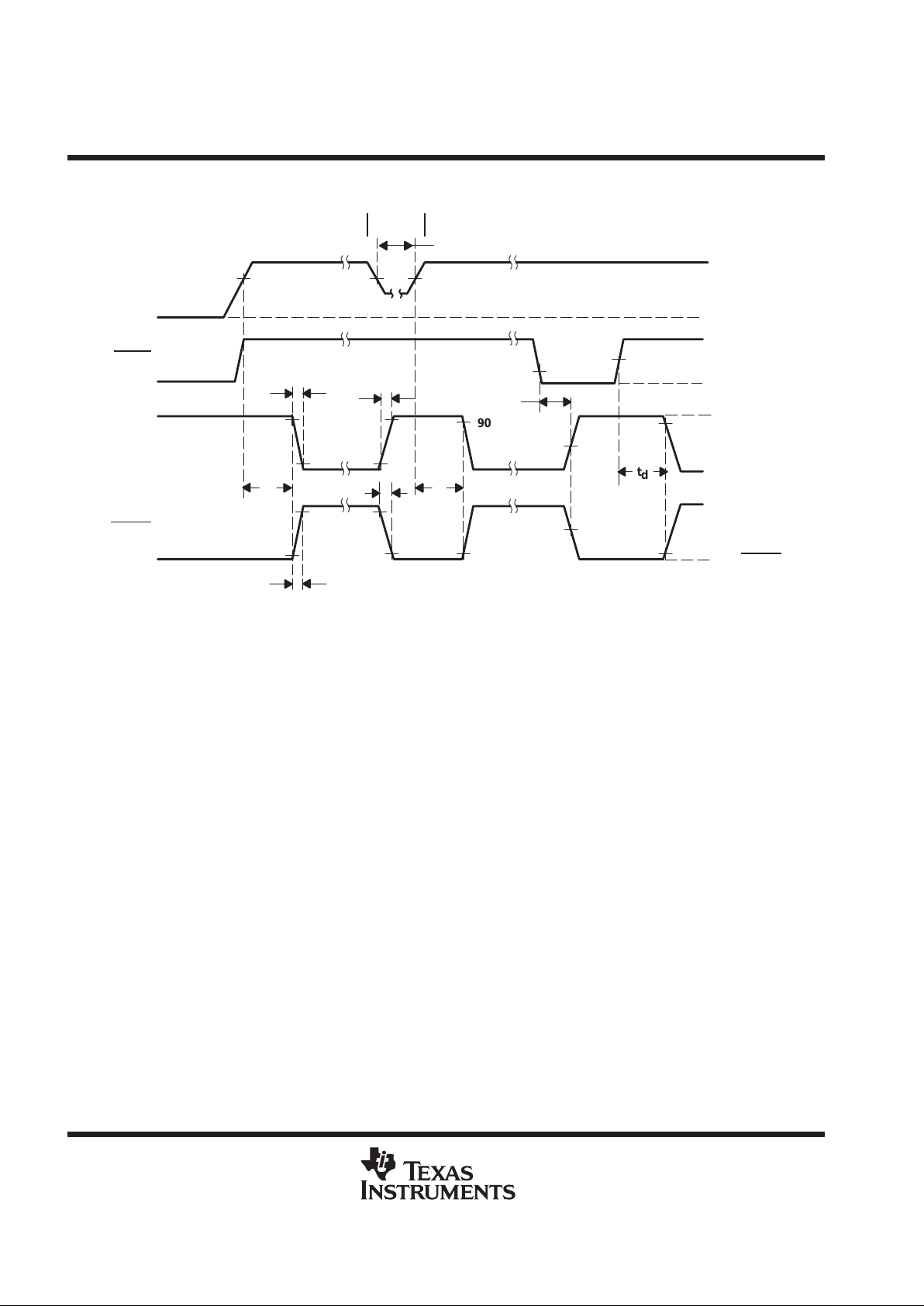
Figure 1. Voltage Waveforms
Page 7
TL7702A, TL7705A, TL7709A, TL7712A, TL7715A
SUPPLY-VOLTAGE SUPERVISORS
SLVS028E – APRIL 1983 – REVISED JULY 1999
7
POST OFFICE BOX 655303 • DALLAS, TEXAS 75265
TYPICAL CHARACTERISTICS
†
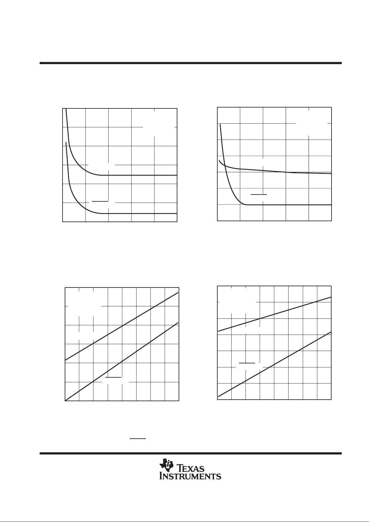
Figure 2
30
26
22
18
0246
34
38
ASSERTION TIME
vs
LOAD RESISTANCE
42
810
t – Assertion Time – ns
RL – Load Resistance – kΩ
RESET t
r
RESET t
f
VCC = 5 V
CT = 0.1 µF
CL = 10 pF
TA = 25°C
Figure 3
4
3
2
1
0246
t – Deassertion Time –
5
6
DEASSERTION TIME
vs
LOAD RESISTANCE
7
810
0
sµ
RL – Load Resistance – kΩ
RESET t
f
RESET t
r
VCC = 5 V
CT = 0.1 µF
CL = 10 pF
TA = 25°C
Figure 4
32
28
24
20
0 25 50 75 100 125
36
40
ASSERTION TIME
vs
LOAD CAPACITANCE
44
150 175 200
RESET t
r
RESET t
f
VCC = 5 V
CT = 0.1 µF
RL = 4.7 kΩ
TA = 25°C
t – Assertion Time – ns
CL – Load Capacitance – pF
Figure 5
2.4
2
1.6
1.2
2.8
3.2
DEASSERTION TIME
vs
LOAD CAPACITANCE
3.6
RESET t
f
RESET t
r
VCC = 5 V
CT = 0.1 µF
RL = 4.7 kΩ
TA = 25°C
0 25 50 75 100 125 150 175 200
CL – Load Capacitance – pF
0.8
t – Deassertion Time – sµ
†
For proper operation, both RESET and RESET should be terminated with resistors of similar value. Failure to do so may cause unwanted
plateauing in either output waveform during switching.
Page 8
TL7702A, TL7705A, TL7709A, TL7712A, TL7715A
SUPPLY-VOLTAGE SUPERVISORS
SLVS028E – APRIL 1983 – REVISED JULY 1999
8
POST OFFICE BOX 655303 • DALLAS, TEXAS 75265
APPLICATION INFORMATION
22 kΩ
0.1 µF
SENSE
RESIN
GND
RESET
RESET
V
CC
CT
System Reset
10 kΩ
C
T
10 kΩ
0.1 µF
SENSE
RESIN
GND
RESET
RESET
V
CC
CT
0.1 µF
SENSE
RESIN
GND
REF
RESET
V
CC
CT
C
T
C
T
5 V
12 V
–12 V
GND
TL7712A
TL7705A
TL7712A
RESET
10 kΩ
10 kΩ
REF
10 kΩ
REF
8
7
2
3
4
1
6
5
8
7
2
3
4
1
6
5
8
7
2
3
4
1
6
5
C
T
(F)
+
t
d(s
)
1.3 10
4
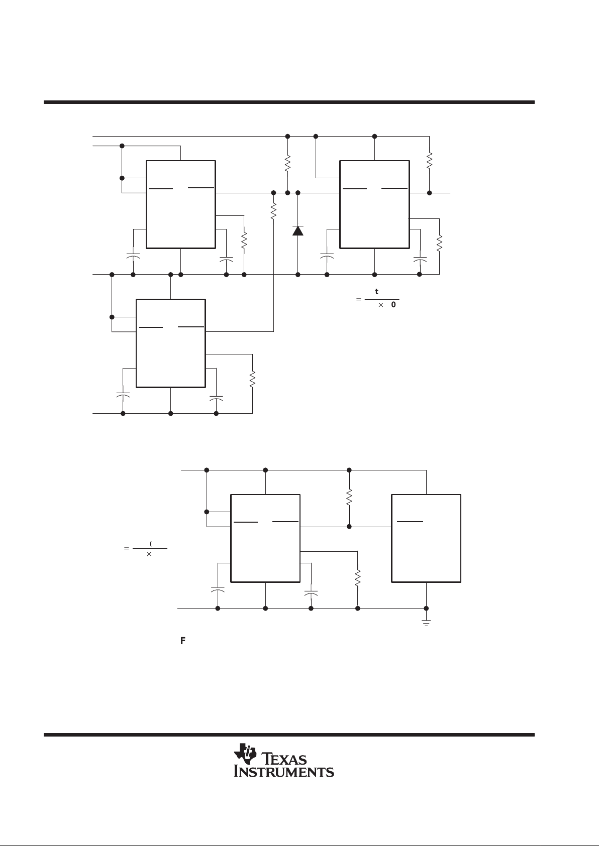
Figure 6. Multiple Power-Supply System Reset Generation
5 V
10 kΩ
0.1 µF
SENSE
RESIN
GND
REF
RESET
V
CC
CT
C
T
RESET
V
CC
GND
V
SS
TMS7000
TL7705A
10 kΩ
RESET
8
7
2
3
4
1
6
5
C
T
(F)
+
t
d(s
)
1.3 10
4
Figure 7. Reset Controller for TMS7000 System
Page 9
TL7702A, TL7705A, TL7709A, TL7712A, TL7715A
SUPPLY-VOLTAGE SUPERVISORS
SLVS028E – APRIL 1983 – REVISED JULY 1999
9
POST OFFICE BOX 655303 • DALLAS, TEXAS 75265
APPLICATION INFORMATION
4.7 kΩ
0.1 µF
SENSE
GND
REF
RESET
V
CC
CT
C
T
TL7705A
INPUT OUTPUT
C
O
C
I
COMMON
25 kΩ
G
S
D
Q1
2N3994
5 V
µA7805
RESET
4.7 kΩ
System RESET
8
7
3
4
1
6
5
Input
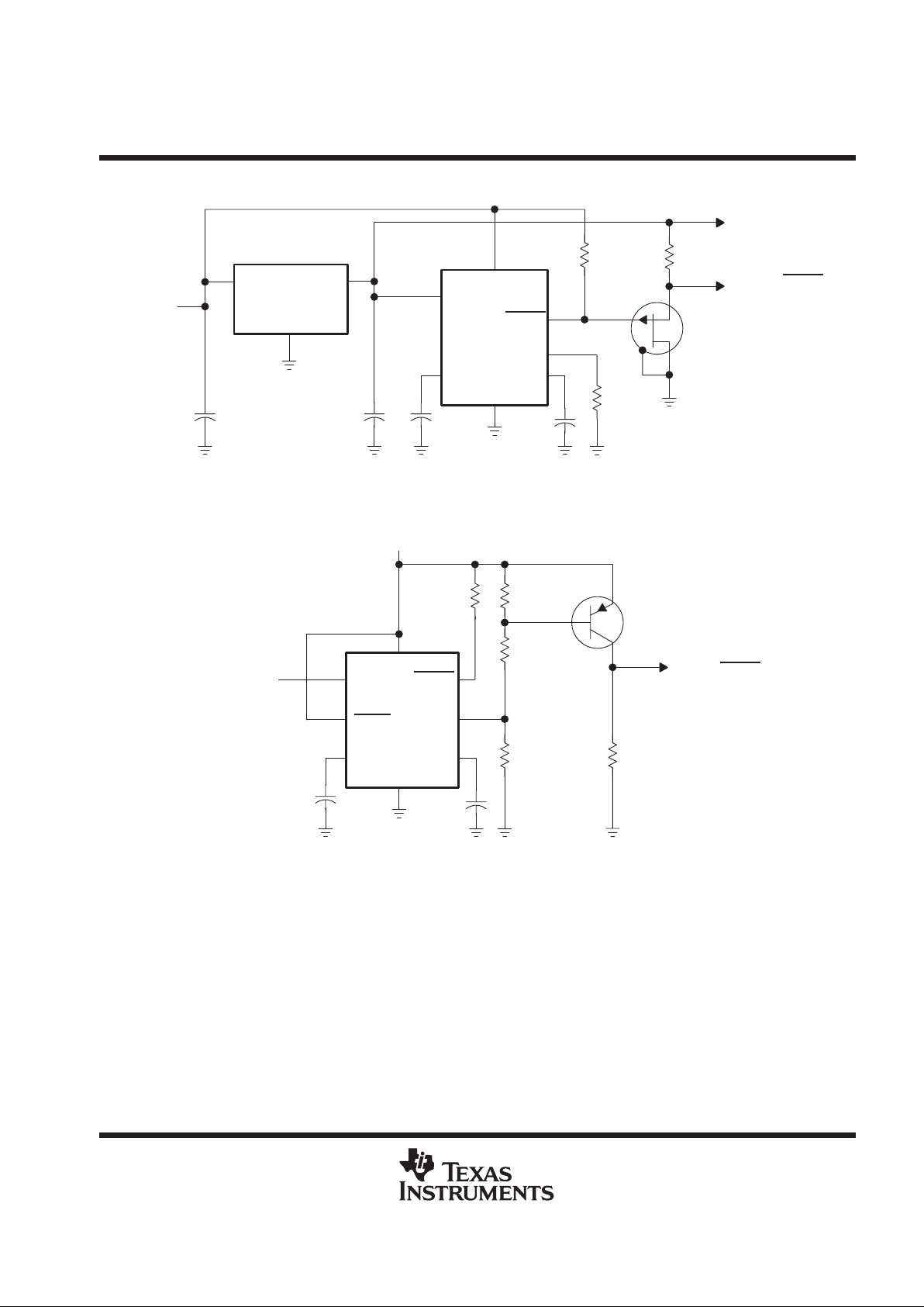
Figure 8. Eliminating Undefined States Using a P-Channel JFET
2.7 kΩ
0.1 µF
SENSE
GND
REF
RESIN
V
CC
CT
C
T
TL77xxA
RESET
750 Ω
System RESET
Q1
2N4036
V
CC
10 kΩ 1 kΩ
10 kΩ
RESET
8
7
3
4
1
6
5
SENSE Input
2
Figure 9. Eliminating Undefined States Using a pnp Transistor
Page 10

IMPORTANT NOTICE
T exas Instruments and its subsidiaries (TI) reserve the right to make changes to their products or to discontinue
any product or service without notice, and advise customers to obtain the latest version of relevant information
to verify, before placing orders, that information being relied on is current and complete. All products are sold
subject to the terms and conditions of sale supplied at the time of order acknowledgement, including those
pertaining to warranty, patent infringement, and limitation of liability.
TI warrants performance of its semiconductor products to the specifications applicable at the time of sale in
accordance with TI’s standard warranty. Testing and other quality control techniques are utilized to the extent
TI deems necessary to support this warranty. Specific testing of all parameters of each device is not necessarily
performed, except those mandated by government requirements.
CERT AIN APPLICATIONS USING SEMICONDUCTOR PRODUCTS MAY INVOL VE POTENTIAL RISKS OF
DEATH, PERSONAL INJURY, OR SEVERE PROPERTY OR ENVIRONMENTAL DAMAGE (“CRITICAL
APPLICATIONS”). TI SEMICONDUCTOR PRODUCTS ARE NOT DESIGNED, AUTHORIZED, OR
WARRANTED TO BE SUITABLE FOR USE IN LIFE-SUPPORT DEVICES OR SYSTEMS OR OTHER
CRITICAL APPLICATIONS. INCLUSION OF TI PRODUCTS IN SUCH APPLICA TIONS IS UNDERSTOOD T O
BE FULLY AT THE CUSTOMER’S RISK.
In order to minimize risks associated with the customer’s applications, adequate design and operating
safeguards must be provided by the customer to minimize inherent or procedural hazards.
TI assumes no liability for applications assistance or customer product design. TI does not warrant or represent
that any license, either express or implied, is granted under any patent right, copyright, mask work right, or other
intellectual property right of TI covering or relating to any combination, machine, or process in which such
semiconductor products or services might be or are used. TI’s publication of information regarding any third
party’s products or services does not constitute TI’s approval, warranty or endorsement thereof.
Copyright 1999, Texas Instruments Incorporated
 Loading...