

Page 1
LM10
Operational Amplifier and Voltage Reference
General Description
The LM10 series are monolithic linear ICs consisting of a
precision reference, an adjustable reference buffer and an
independent, high quality op amp.
The unit can operate from a total supply voltage as low as
1.1V or as high as 40V, drawing only 270µA. Acomplementary output stage swings within 15 mV of the supply terminals or will deliver
±
20 mA output current with±0.4V satura-
tion. Reference output can be as low as 200 mV.
The circuit is recommended for portable equipment and is
completely specified for operation from a single power cell.
In contrast, high output-drive capability, both voltage and
current, along with thermal overload protection, suggest it in
demanding general-purpose applications.
The device is capable of operating in a floating mode, independent of fixed supplies. It can function as a remote comparator, signal conditioner, SCR controller or transmitter for
analog signals, delivering the processed signal on the same
line used to supply power. It is also suited for operation in a
wide range of voltage- and current-regulator applications,
from low voltages to several hundred volts, providing greater
precision than existing ICs.
This series is available in the three standard temperature
ranges, with the commercial part having relaxed limits. In addition, a low-voltage specification (suffix “L”) is available in
the limited temperature ranges at a cost savings.
Features
n input offset voltage: 2.0 mV (max)
n input offset current: 0.7 nA (max)
n input bias current: 20 nA (max)
n reference regulation: 0.1%(max)
n offset voltage drift: 2µV/˚C
n reference drift: 0.002%/˚C
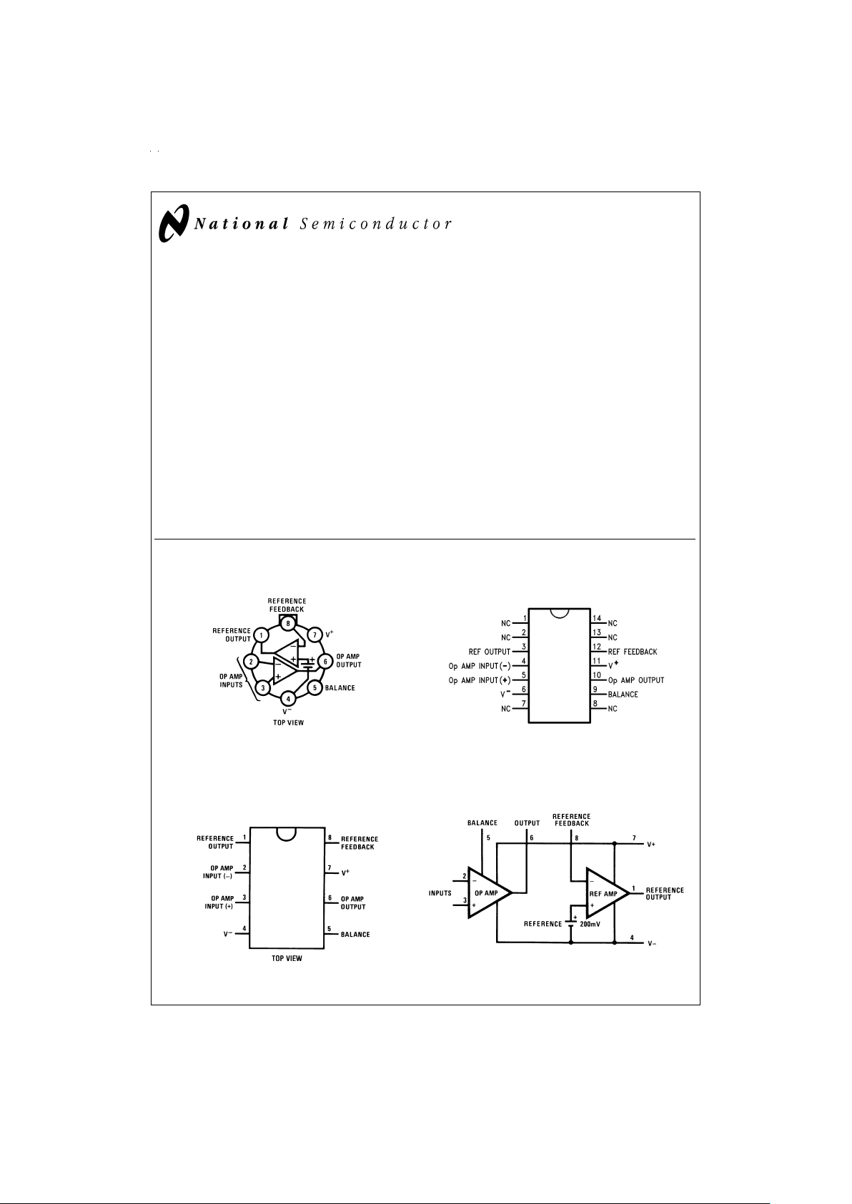
Connection and Functional Diagrams
Metal Can Package (H)
DS005652-1
Order Number LM10BH, LM10CH,
LM10CLH or LM10H/883
available per SMA
#
5962-8760401
See NS Package Number H08A
Small Outline Package (WM)
DS005652-17
Order Number LM10CWM
See NS Package Number M14B
Dual-In-Line Package (N)
DS005652-15
Order Number LM10CN or LM10CLN
See NS Package Number N08E
DS005652-16
May 1998
LM10 Operational Amplifier and Voltage Reference
© 1999 National Semiconductor Corporation DS005652 www.national.com
Page 2
Absolute Maximum Ratings (Notes 1, 8)
If Military/Aerospace specified devices are required,
please contact the National Semiconductor Sales Office/
Distributors for availability and specifications.
LM10/LM10B/ LM10BL/
LM10C LM10CL
Total Supply Voltage 45V 7V
Differential Input Voltage (Note 2)
±
40V
±
7V
Power Dissipation (Note 3) internally limited
Output Short-circuit Duration (Note 4) continuous
Storage-Temp. Range −55˚C to +150˚C
Lead Temp. (Soldering, 10 seconds)
Metal Can 300˚C
Lead Temp. (Soldering, 10 seconds) DIP 260˚C
Vapor Phase (60 seconds) 215˚C
Infrared (15 seconds) 220˚C
See AN-450 “Surface Mounting Methods and Their Effect on
Product Reliability” for other methods of soldering surface
mount devices.
ESD rating is to be determined.
Maximum Junction Temperature
LM10 150˚C
LM10B 100˚C
LM10C 85˚C
Operating Ratings
Package Thermal Resistance
θ
JA
H Package 150˚C/W
N Package 87˚C/W
WM Package 90˚C/W
θ
JC
H Package 45˚C/W
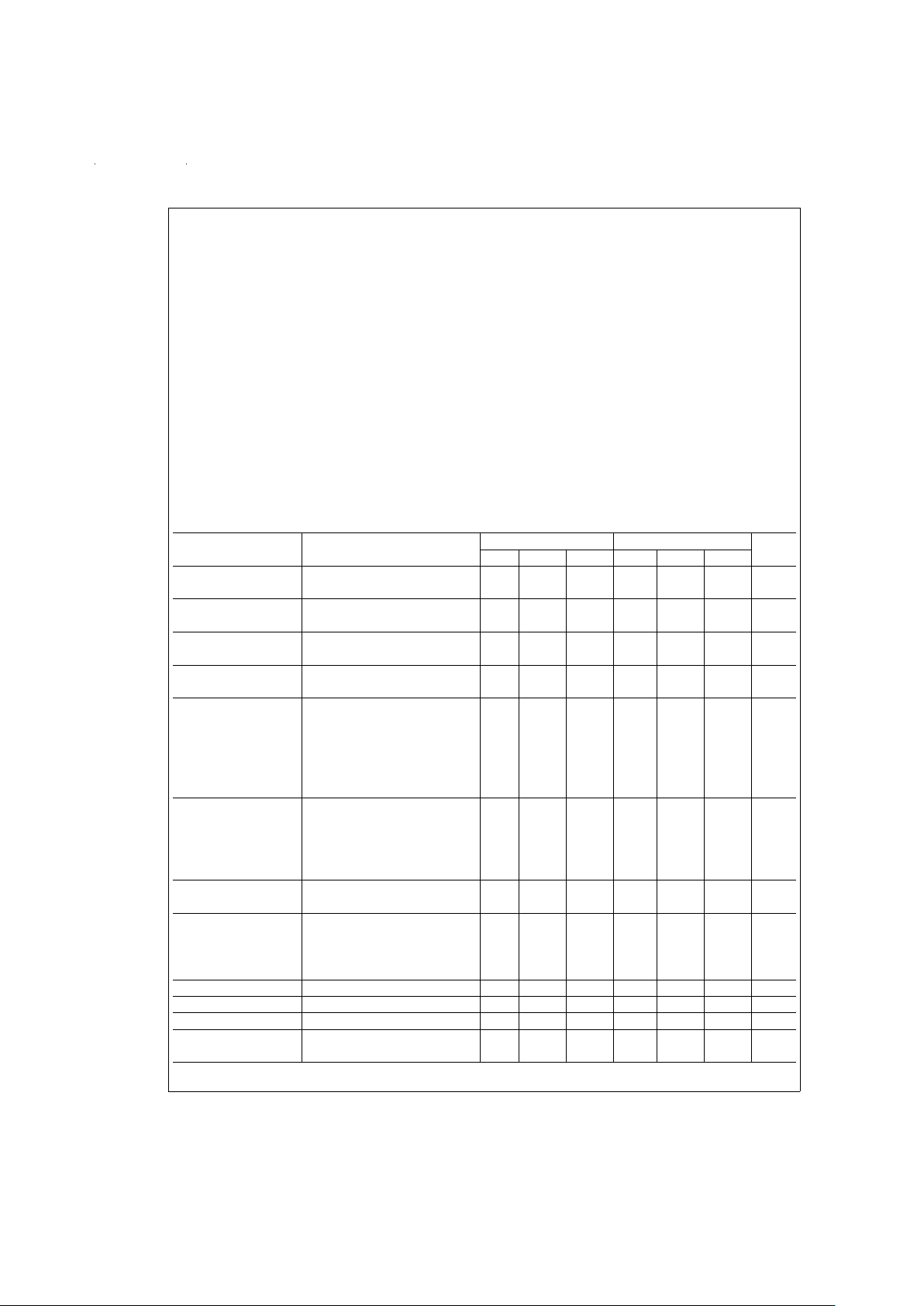
Electrical Characteristics
T
J
=
25˚C, T
MIN≤TJ≤TMAX
(Boldface type refers to limits over temperature range) (Note 5)
Parameter Conditions LM10/LM10B LM10C Units
Min Typ Max Min Typ Max
Input offset voltage 0.3 2.0 0.5 4.0 mV
3.0 5.0 mV
Input offset current 0.25 0.7 0.4 2.0 nA
(Note 6) 1.5 3.0 nA
Input bias current 10 20 12 30 nA
30 40 nA
Input resistance 250 500 150 400 kΩ
150 115 kΩ
Large signal voltage V
S
=
±
20V, I
OUT
=
0 120 400 80 400 V/mV
gain V
OUT
=
±
19.95V 80 50 V/mV
V
S
=
±
20V, V
OUT
=
±
19.4V 50 130 25 130 V/mV
I
OUT
=
±
20 mA (±15 mA) 20 15 V/mV
V
S
=
±
0.6V (0.65V), I
OUT
=
±
2 mA 1.5 3.0 1.0 3.0 V/mV
V
OUT
=
±
0.4V (±0.3V), V
CM
=
−0.4V 0.5 0.75 V/mV
Shunt gain (Note 7) 1.2V (1.3V) ≤V
OUT
≤40V, 14 33 10 33 V/mV
R
L
=
1.1 kΩ
0.1 mA≤I
OUT
≤5mA 66V/mV
1.5V≤V
+
≤40V, R
L
=
250Ω 8 25 6 25 V/mV
0.1 mA≤I
OUT
≤20 mA 44V/mV
Common-mode −20V≤V
CM
≤19.15V (19V) 93 102 90 102 dB
rejection V
S
=
±
20V 87 87 dB
Supply-voltage −0.2V≥V
−
≥−39V 90 96 87 96 dB
rejection V
+
=
1.0V (1.1V) 84 84 dB
1.0V (1.1V) ≤V
+
≤39.8V 96 106 93 106 dB
V
−
=
−0.2V 90 90 dB
Offset voltage drift 2.0 5.0 µV/˚C
Offset current drift 2.0 5.0 pA/˚C
Bias current drift T
C
<
100˚C 60 90 pA/˚C
Line regulation 1.2V (1.3V) ≤V
S
≤40V 0.001 0.003 0.001 0.008
%
/V
0≤I
REF
≤1.0 mA, V
REF
=
200 mV 0.006 0.01
%
/V
www.national.com 2
Page 3
Electrical Characteristics (Continued)
T
J
=
25˚C, T
MIN≤TJ≤TMAX
(Boldface type refers to limits over temperature range) (Note 5)
Parameter Conditions LM10/LM10B LM10C Units
Min Typ Max Min Typ Max
Load regulation 0≤I
REF
≤1.0 mA 0.01 0.1 0.01 0.15
%
V
+
−V
REF
≥1.0V (1.1V) 0.15 0.2
%
Amplifier gain 0.2V≤V
REF
≤35V 50 75 25 70 V/mV
23 15 V/mV
Feedback sense 195 200 205 190 200 210 mV
voltage 194 206 189 211 mV
Feedback current 20 50 22 75 nA
65 90 nA
Reference drift 0.002 0.003
%
/˚C
Supply current 270 400 300 500 µA
500 570 µA
Supply current change 1.2V (1.3V) ≤V
S
≤40V 15 75 15 75 µA
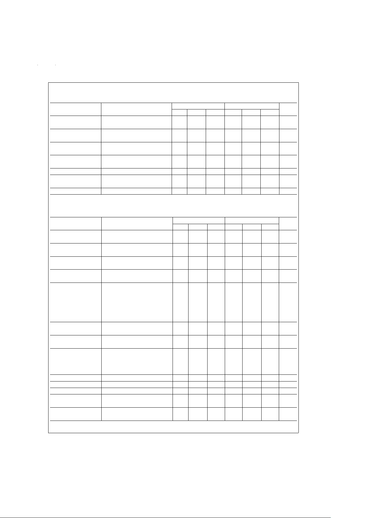
Electrical Characteristics
T
J
=
25˚C, T
MIN≤TJ≤TMAX
(Boldface type refers to limits over temperature range) (Note 5)
Parameter Conditions LM10BL LM10CL Units
Min Typ Max Min Typ Max
Input offset voltage 0.3 2.0 0.5 4.0 mV
3.0 5.0 mV
Input offset current 0.1 0.7 0.2 2.0 nA
(Note 6) 1.5 3.0 nA
Input bias current 10 20 12 30 nA
30 40 nA
Input resistance 250 500 150 400 kΩ
150 115 kΩ
Large signal voltage V
S
=
±
3.25V, I
OUT
=
0 60 300 40 300 V/mV
gain V
OUT
=
±
3.2V 40 25 V/mV
V
S
=
±
3.25V, I
OUT
=
10 mA 10 25 5 25 V/mV
V
OUT
=
±
2.75 V 43V/mV
V
S
=
±
0.6V (0.65V), I
OUT
=
±
2 mA 1.5 3.0 1.0 3.0 V/mV
V
OUT
=
±
0.4V (±0.3V), V
CM
=
−0.4V 0.5 0.75 V/mV
Shunt gain (Note 7) 1.5V≤V
+
≤6.5V, R
L
=
500Ω 8 30 6 30 V/mV
0.1 mA≤I
OUT
≤10 mA 44V/mV
Common-mode −3.25V≤V
CM
≤2.4V (2.25V) 89 102 80 102 dB
rejection V
S
=
±
3.25V 83 74 dB
Supply-voltage −0.2V≥V
−
≥−5.4V 86 96 80 96 dB
rejection V
+
=
1.0V (1.2V) 80 74 dB
1.0V (1.1V) ≤V
+
≤6.3V 94 106 80 106 dB
V
−
=
0.2V 88 74 dB
Offset voltage drift 2.0 5.0 µV/˚C
Offset current drift 2.0 5.0 pA/˚C
Bias current drift 60 90 pA/˚C
Line regulation 1.2V (1.3V) ≤V
S
≤6.5V 0.001 0.01 0.001 0.02
%
/V
0≤I
REF
≤0.5 mA, V
REF
=
200 mV 0.02 0.03
%
/V
Load regulation 0≤I
REF
≤0.5 mA 0.01 0.1 0.01 0.15
%
V
+
−V
REF
≥1.0V (1.1V) 0.15 0.2
%
www.national.com3
Page 4
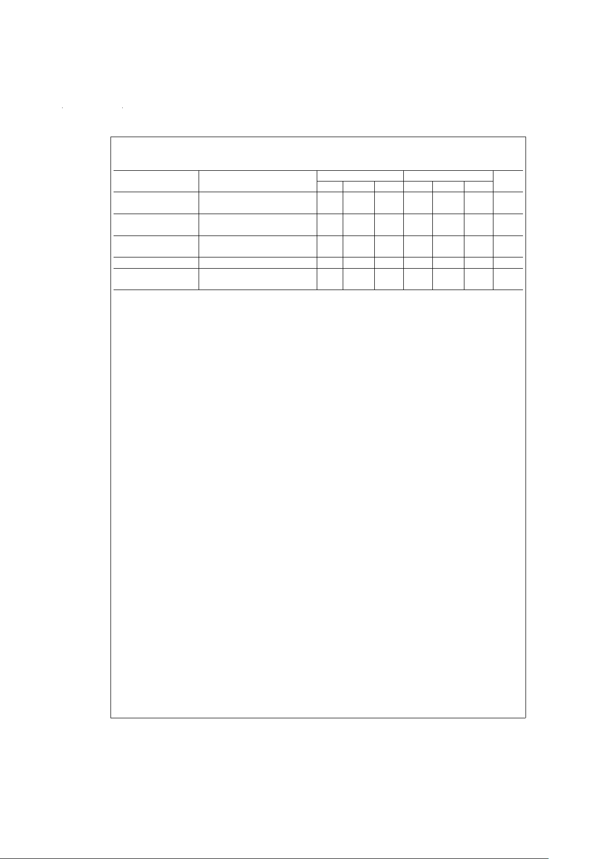
Electrical Characteristics (Continued)
T
J
=
25˚C, T
MIN≤TJ≤TMAX
(Boldface type refers to limits over temperature range) (Note 5)
Parameter Conditions LM10BL LM10CL Units
Min Typ Max Min Typ Max
Amplifier gain 0.2V≤V
REF
≤5.5V 30 70 20 70 V/mV
20 15 V/mV
Feedback sense voltage 195 200 205 190 200 210 mV
194 206 189 211 mV
Feedback current 20 50 22 75 nA
65 90 nA
Reference drift 0.002 0.003
%
/˚C
Supply current 260 400 280 500 µA
500 570 µA
Note 1: Absolute Maximum Ratings indicatelimitsbeyondwhichdamagetothe device may occur. Operating Ratings indicateconditionsforwhichthedevice is func-
tional, but do not guarantee specific performance limits.
Note 2: The Input voltage can exceed the supply voltages provided that the voltage from the input to any other terminal does not exceed the maximum differential
input voltage and excess dissipation is accounted for when V
IN
<
V−.
Note 3: The maximum, operating-junction temperature is 150˚C for the LM10, 100˚C for the LM10B(L) and 85˚C for the LM10C(L). At elevated temperatures, devices
must be derated based on package thermal resistance.
Note 4: Internal thermal limiting prevents excessive heating that could result in sudden failure, but the IC can be subjected to accelerated stress with a shorted output
and worst-case conditions.
Note 5: These specifications apply for V
−
≤VCM≤V+−0.85V (1.0V), 1.2V (1.3V)<VS≤V
MAX,VREF
=
0.2V and 0≤I
REF
≤1.0 mA, unless otherwise specified: V
MAX
=
40V
for the standard part and 6.5V for the low voltage part. Normal typeface indicates 25˚C limits. Boldface type indicates limits and altered test conditions for
full-temperature-range operation; this is −55˚C to 125˚C for the LM10, −25˚C to 85˚C for the LM10B(L) and 0˚C to 70˚C for the LM10C(L). The specifications do
not include the effects of thermal gradients (τ
1
≅
20 ms), die heating (τ
2
≅
0.2s) or package heating. Gradient effects are small and tend to offset the electrical error (see
curves).
Note 6: For T
J
>
90˚C, IOSmay exceed 1.5 nA for V
CM
=
V
−
. With T
J
=
125˚C and V
−
≤VCM≤V−+0.1V, IOS≤5 nA.
Note 7: This defines operation in floating applications such as the bootstrapped regulator or two-wire transmitter. Output is connected to the V
+
terminal of the IC
and input common mode is referred to V
−
(see typical applications). Effect of larger output-voltage swings with higher load resistance can be accounted for by adding
the positive-supply rejection error.
Note 8: Refer to RETS10X for LM10H military specifications.
Definition of Terms
Input offset voltage: That voltage which must be applied
between the input terminals to bias the unloaded output in
the linear region.
Input offset current: The difference in the currents at the input terminals when the unloaded output is in the linear region.
Input bias current: The absolute value of the average of the
two input currents.
Input resistance: The ratio of the change in input voltage to
the change in input current on either input with the other
grounded.
Large signal voltage gain: The ratio of the specified output
voltage swing to the change in differential input voltage required to produce it.
Shunt gain: The ratio of the specified output voltage swing
to the change in differential input voltage required to produce
it with the output tied to the V
+
terminal of the IC. The load
and power source are connected between the V
+
and V−ter-
minals, and input common-mode is referred to the V
−
termi-
nal.
Common-mode rejection: The ratio of the input voltage
range to the change in offset voltage between the extremes.
Supply-voltage rejection: The ratio of the specified
supply-voltage change to the change in offset voltage between the extremes.
Line regulation: The average change in reference output
voltage over the specified supply voltage range.
Load regulation: The change in reference output voltage
from no load to that load specified.
Feedback sense voltage: The voltage, referred to V
−
,on
the reference feedback terminal while operating in regulation.
Reference amplifier gain: The ratio of the specified reference output change to the change in feedback sense voltage
required to produce it.
Feedback current: The absolute value of the current at the
feedback terminal when operating in regulation.
Supply current: The current required from the power
source to operate the amplifier and reference with their outputs unloaded and operating in the linear range.
www.national.com 4
Page 5
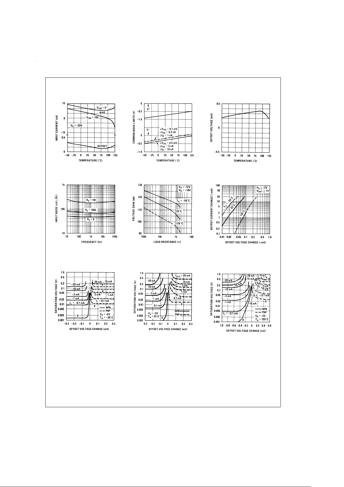
Typical Performance Characteristics (Op Amp)
Input Current
DS005652-18
Common Mode Limits
DS005652-19
Output Voltage Drift
DS005652-20
Input Noise Voltage
DS005652-21
DC Voltage Gain
DS005652-22
Transconductance
DS005652-23
Output Saturation
Characteristics
DS005652-24
Output Saturation
Characteristics
DS005652-25
Output Saturation
Characteristics
DS005652-26
www.national.com5
Page 6
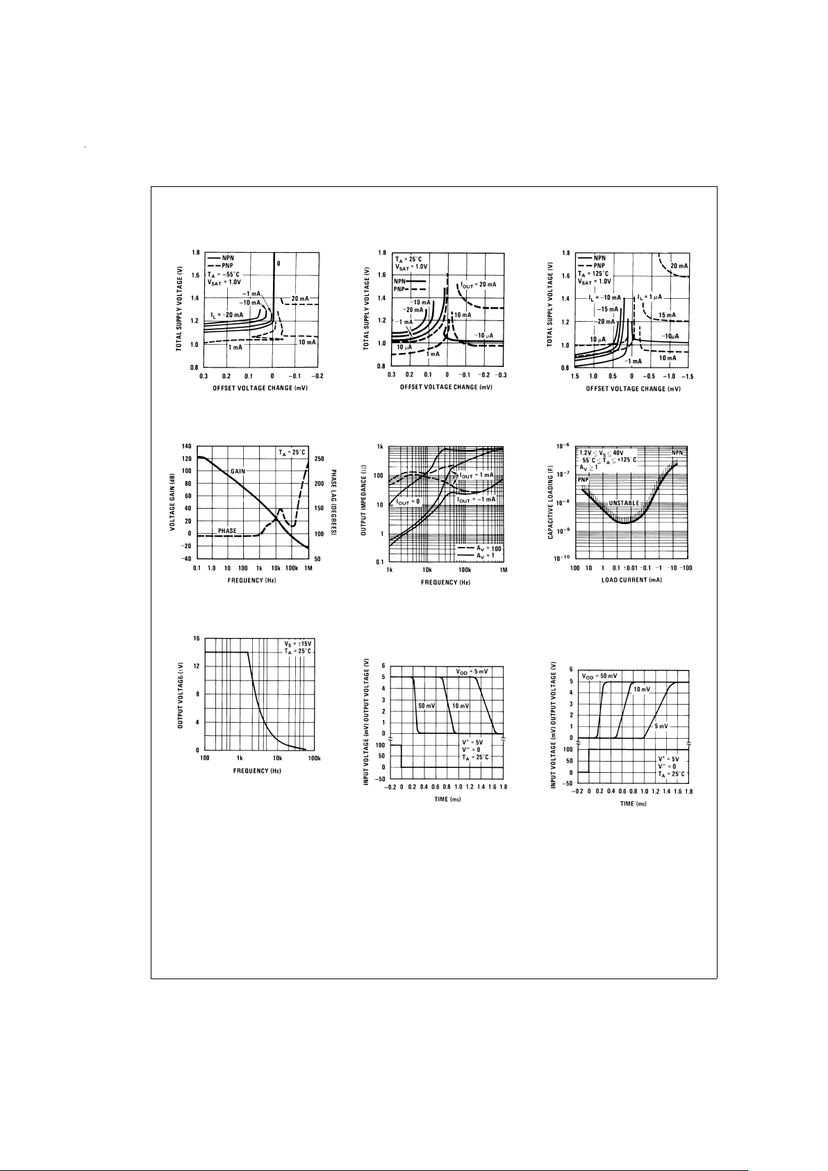
Typical Performance Characteristics (Op Amp) (Continued)
Minimum Supply Voltage
DS005652-27
Minimum Supply Voltage
DS005652-28
Minimum Supply Voltage
DS005652-29
Frequency Response
DS005652-30
Output Impedance
DS005652-31
Typical Stability Range
DS005652-32
Large Signal Response
DS005652-33
Comparator Response
Time For Various
Input Overdrives
DS005652-34
Comparator Response
Time For Various
Input Overdrives
DS005652-35
www.national.com 6
Page 7
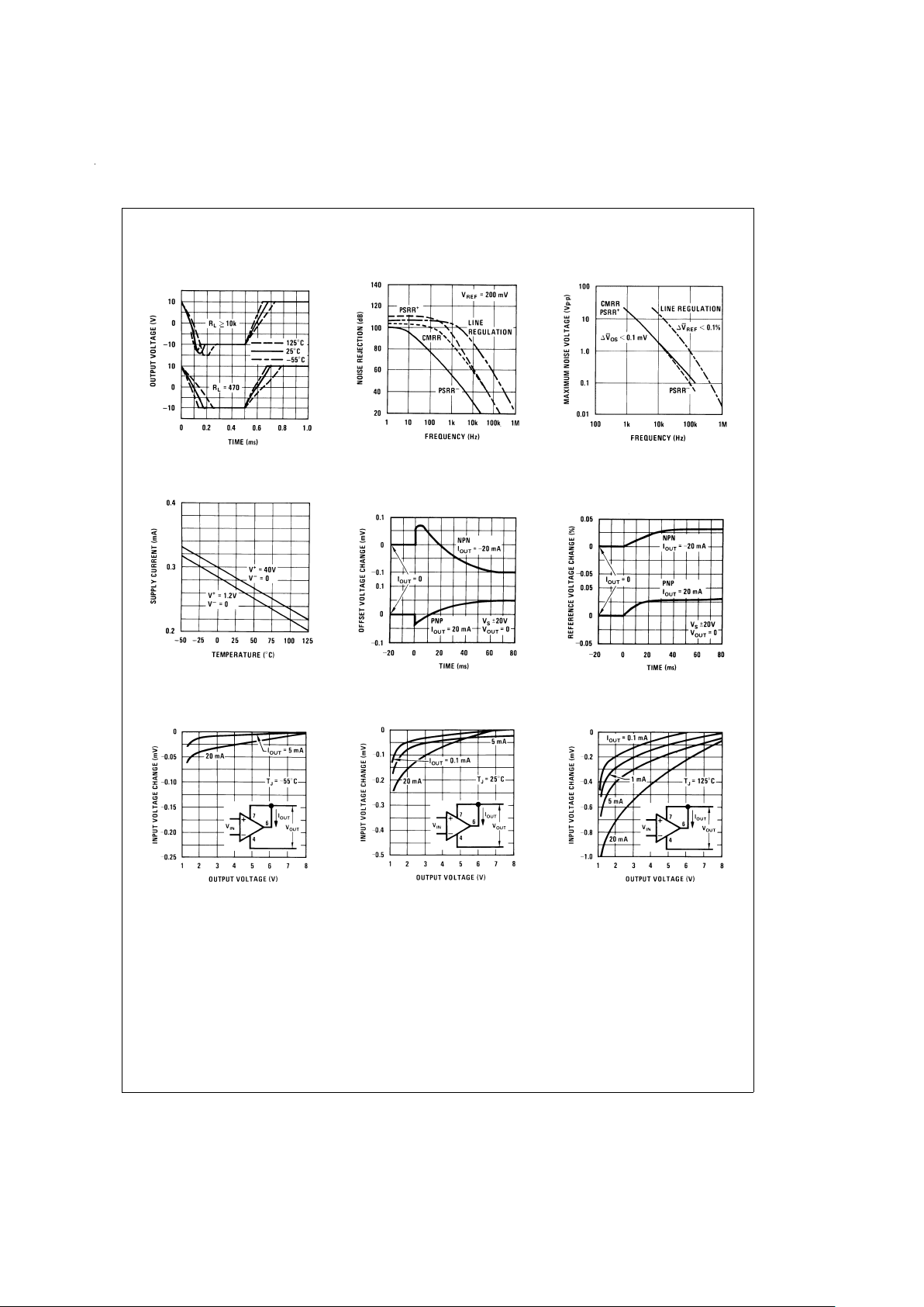
Typical Performance Characteristics (Op Amp) (Continued)
Follower Pulse
Response
DS005652-36
Noise Rejection
DS005652-37
Rejection Slew Limiting
DS005652-38
Supply Current
DS005652-39
Thermal Gradient
Feedback
DS005652-40
Thermal Gradient
Cross-coupling
DS005652-41
Shunt Gain
DS005652-42
Shunt Gain
DS005652-43
Shunt Gain
DS005652-44
www.national.com7
Page 8

Typical Performance Characteristics (Reference)
Typical Applications
(Note 10) (Pin numbers are for devices in 8-pin packages)
Op Amp Offset Adjustment
Line Regulation
DS005652-45
Load Regulation
DS005652-46
Reference Noise Voltage
DS005652-47
Minimum Supply Voltage
DS005652-48
Output Saturation
DS005652-49
Typical Stability Range
DS005652-50
Standard
DS005652-51
Limited Range
DS005652-52
Limited Range With Boosted
Reference
DS005652-53
www.national.com 8
Page 9

Typical Applications (Note 10) (Pin numbers are for devices in 8-pin packages) (Continued)
Positive Regulators (Note 9)
Low Voltage
DS005652-54
Best Regulation
DS005652-55
Zero Output
DS005652-56
Note 9: Use only electrolytic output capacitors.
Current Regulator
DS005652-57
Shunt Regulator
DS005652-58
Required For Capacitive Loading
Negative Regulator
DS005652-59
*Electrolytic
Precision Regulator
DS005652-60
www.national.com9
Page 10

Typical Applications (Note 10) (Pin numbers are for devices in 8-pin packages) (Continued)
Laboratory Power Supply
DS005652-61
*V
OUT
=
10
−4
R3
HV Regulator
DS005652-62
DS005652-84
www.national.com 10
Page 11

Typical Applications (Note 10) (Pin numbers are for devices in 8-pin packages) (Continued)
Protected HV Regulator
DS005652-63
Flame Detector
DS005652-64
*800˚C Threshold Is Established By Connecting Balance To V
REF
.
Light Level Sensor
DS005652-65
*Provides Hysteresis
Remote Amplifier
DS005652-66
Remote Thermocouple Amplifier
DS005652-67
www.national.com11
Page 12

Typical Applications (Note 10) (Pin numbers are for devices in 8-pin packages) (Continued)
Transmitter for Bridge Sensor
DS005652-68
Precision Thermocouple Transmitter
DS005652-69
10 mA≤I
OUT
≤50 mA
500˚C≤T
P
≤1500˚C
*Gain Trim
www.national.com 12
Page 13

Typical Applications (Note 10) (Pin numbers are for devices in 8-pin packages) (Continued)
Resistance Thermometer Transmitter
DS005652-70
Optical Pyrometer
DS005652-71
††
Level-shift Trim
*Scale Factor Trim
†
Copper Wire Wound
Thermocouple Transmitter
DS005652-72
200˚C≤Tp≤700˚C
1mA≤I
OUT
≤5mA
†
Gain Trim
Logarithmic Light Sensor
DS005652-73
1mA≤I
OUT
≤5mA
‡
50 µA≤ID≤500 µA
††
Center Scale Trim
†
Scale Factor Trim
*
Copper Wire Wound
www.national.com13
Page 14

Typical Applications (Note 10) (Pin numbers are for devices in 8-pin packages) (Continued)
Battery-level Indicator
DS005652-74
Battery-threshold Indicator
DS005652-75
Single-cell Voltage Monitor
DS005652-76
Flashes Above 1.2V
Rate Increases With
Voltage
Double-ended Voltage Monitor
DS005652-77
Flash Rate Increases
Above 6V and Below 15V
Meter Amplifier
DS005652-78
INPUT
10 mV, 100nA
FULL-SCALE
www.national.com 14
Page 15

Typical Applications (Note 10) (Pin numbers are for devices in 8-pin packages) (Continued)
Thermometer
DS005652-79
*Trim For Span
†
Trim For Zero
Light Meter
DS005652-80
1≤λ/λ0≤10
5
www.national.com15
Page 16

Typical Applications (Note 10) (Pin numbers are for devices in 8-pin packages) (Continued)
Microphone Amplifier
DS005652-81
Z
OUT
z
680Ω@5 kHz
A
V
≤1k
f
1
z
100 Hz
f
2
z
5 kHz
R
L
z
500
*Max Gain Trim
Isolated Voltage Sensor
DS005652-82
†
Controls “Loop Gain”
*Optional Frequency Shaping
www.national.com 16
Page 17

Typical Applications (Note 10) (Pin numbers are for devices in 8-pin packages) (Continued)
Note 10: Circuit descriptions available in application note AN-211.
Application Hints
With heavy amplifier loading to V−, resistance drops in the V−lead can adversely affect reference regulation. Lead resistance can
approach 1Ω. Therefore, the common to the reference circuitry should be connected as close as possible to the package.
Light-level Controller
DS005652-83
www.national.com17
Page 18

Operational Amplifier Schematic (Pin numbers are for 8-pin packages)
DS005652-13
www.national.com 18
Page 19

Reference and Internal Regulator (Pin numbers are for 8-pin packages)
DS005652-14
www.national.com19
Page 20

Physical Dimensions inches (millimeters) unless otherwise noted
Metal Can Package (H)
Order Number LM10BH, LM10CH, LM10CLH or LM10H/883
NS Package Number H08A
S.O. Package (WM)
Order Number LM10CWM
NS Package Number M14B
www.national.com 20
Page 21

Physical Dimensions inches (millimeters) unless otherwise noted (Continued)
LIFE SUPPORT POLICY
NATIONAL’S PRODUCTS ARE NOT AUTHORIZED FOR USE AS CRITICAL COMPONENTS IN LIFE SUPPORT
DEVICES OR SYSTEMS WITHOUT THE EXPRESS WRITTEN APPROVAL OF THE PRESIDENT OF NATIONAL
SEMICONDUCTOR CORPORATION. As used herein:
1. Life support devices or systems are devices or
systems which, (a) are intended for surgical implant
into the body, or (b) support or sustain life, and
whose failure to perform when properly used in
accordance with instructions for use provided in the
labeling, can be reasonably expected to result in a
significant injury to the user.
2. A critical component is any component of a life
support device or system whose failure to perform
can be reasonably expected to cause the failure of
the life support device or system, or to affect its
safety or effectiveness.
National Semiconductor
Corporation
Americas
Tel: 1-800-272-9959
Fax: 1-800-737-7018
Email: support@nsc.com
National Semiconductor
Europe
Fax: +49 (0) 1 80-530 85 86
Email: europe.support@nsc.com
Deutsch Tel: +49 (0) 1 80-530 85 85
English Tel: +49 (0) 1 80-532 78 32
Français Tel: +49 (0) 1 80-532 93 58
Italiano Tel: +49 (0) 1 80-534 16 80
National Semiconductor
Asia Pacific Customer
Response Group
Tel: 65-2544466
Fax: 65-2504466
Email: sea.support@nsc.com
National Semiconductor
Japan Ltd.
Tel: 81-3-5639-7560
Fax: 81-3-5639-7507
www.national.com
Dual-In-Line Package (N)
Order Number LM10CN or LM10CLN
NS Package Number N08E
LM10 Operational Amplifier and Voltage Reference
National does not assume any responsibility for use of any circuitry described, no circuit patent licenses are implied and National reserves the right at any time without notice to change said circuitry and specifications.
 Loading...