

Page 1
54LVTH162373
3.3V 16-Bit Transparent
D-Type Latches
PRELIMINARY
1OE
1Q1
1Q2
GND
1Q3
1Q4
VCC
1Q5
1Q6
GND
1Q7
1Q8
2Q1
2Q2
GND
2Q3
2Q4
VCC
2Q5
2Q6
GND
2Q7
2Q8
148
54LVTH162373
24 25
1LE
1D1
1D2
GND
1D3
1D4
VCC
1D5
1D6
GND
1D7
1D8
2D1
2D2
GND
2D3
2D4
VCC
2D5
2D6
GND
2D7
2D8
2LE2OE
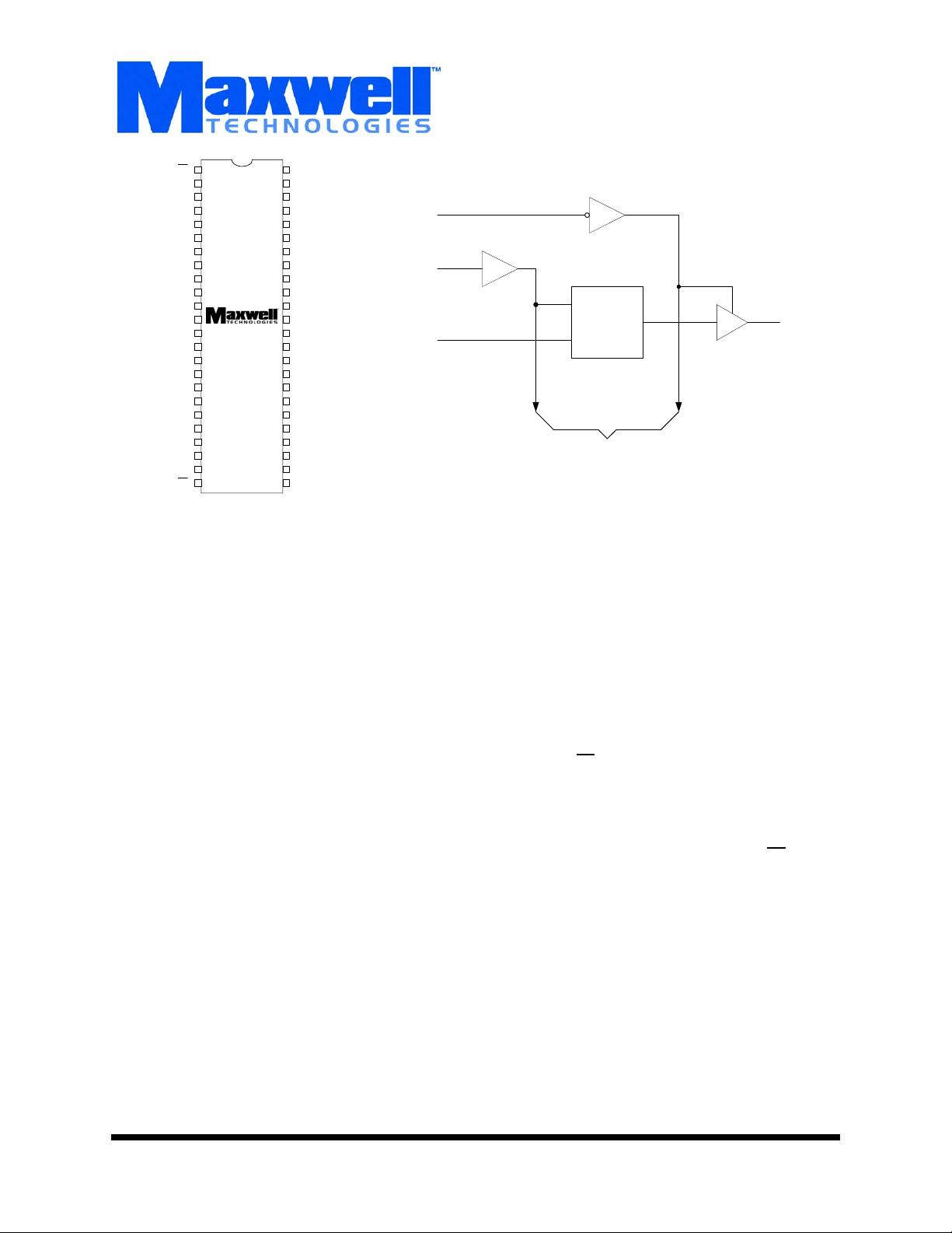
Logic Diagram (PositiveLogic)
1OE/2OE
1LE/2LE
1D1/2D1
FEATURES:
• 3.3V low voltage advanced BiCMOS technology (LVT) 16bit transparent D-type latches with 3-state outputs
• Total dose hardness:
- > 100 krad (Si), depending upon space mission
• Excellent Single Event Effect:
- SEL
: No LU > 119 MeV/mg/cm
TH
• Package: 48 pin RAD-PAK® flat package
• Operating temperature range:
- 55 to 125
• Distributed V
°
C
and GND pin configuration minimizes high-
CC
speed switching noise
• Supports mixed-mode signal operation
- 5V input and output voltages with 3.3V V
• Supports unregulated battery operation down to 2.7V
• Supports live insertion
• Bus-hold data inputs eliminate the need for external pullup
resistors
2
CC
1/24
48/25
47/36
C1
1D
To Seven Other Channels
2/13
1Q1/2Q1
Logic Diagram
DESCRIPTION:
Maxwell Technologies’ 54LVTH162373 16-bit transparent Dtype latches with 3-state output features a greater than 100
krad (Si) total dose tolerance, depending upon space mission.
The 54LVTH162373 is designed for low voltage (3.3V) V
operation, but with the capability to provide a TTL interface to
a 5V system environment. It is suitable for implementing buffer
registers, I/O ports, bidirectional bus drivers, and working registers. The 54LVTH162373 can be used as two 8-bit latches or
one 16-bit latch. When the latch-enable (LE) input is low, the
Q output are latched at the levels set up at the data (D) inputs.
When LE is high, the Q outputs follow the D inputs. A buffered
output-enable (OE
) input can be used to place the eight outputs in either a normal logic state or a high impedance state.
In the high impedance state, the outputs neither load nor drive
the bus lines significantly. The high impedance state and the
increased drive provide the capability to drive bus lines without the need for interface or pullup components. OE
affect internal operations of the latch. Old data can be retained
or new data can be entered while the outputs are in the high
impedance state.
CC
does not
Memory
1000596
(858) 503-3300 - Fax: (858) 503-3301 - www.maxwell.com
Maxwell Technologies' patented R
ogy incorporates radiation shielding in the microcircuit package. It eliminates the need for box shielding while providing
the required radiation shielding for a lifetime in orbit or space
mission. In a GEO orbit, R
krad (Si) radiation dose tolerance. This product is available
with screening up to Class S.
12.19.01 Rev 1
AD-PAK® packaging technol-
AD-PAK provides greater than 100
All data sheets are subject to change without notice
©2001 Maxwell Technologies
All rights reserved.
1
Page 2
3.3V 16-Bit Transparent D-Type
54LVTH162373
PRELIMINARY
TABLE 1. PINOUT DESCRIPTION
PIN SYMBOL DESCRIPTION
1, 24 1OE-2OE Output Enable
2, 3, 5, 6, 8, 9, 11, 12 1Q1-1Q8 Outputs
4, 10, 15, 21, 28, 34, 39, 45 GND Ground
7, 31, 42 V
CC
13, 14, 16, 17, 19, 20, 22, 23 2Q1-2Q8 Outputs
25, 48 2LE-1LE Latch Enable
26, 27, 29, 30, 32, 31, 32,
2D8-2D1 Inputs
33, 35, 36
37, 38, 40, 41, 43, 44, 46, 47 1D8-1D1 Inputs
TABLE 2. 54LVTH162373 ABSOLUTE MAXIMUM RATINGS
PARAMETER SYMBOL MIN MAX UNIT
Supply voltage range V
Input voltage range
Voltage range applied to any output in the high state or power-off
1
state
Current into any output in the low state I
Current into any output in the high state
Input clamp current (V
Output clamp current (V
Maximum power dissipation at TA = 55
Storage temperature range T
1
2
< 0) I
I
< O) IOK -- -50 mA
O
°C 3
Power Supply
CC
V
I
V
O
O
I
O
IK
P
D
S
-0.5 4.6 V
-0.5 7 V
-0.5 7 V
-- 30 mA
-- 30 mA
-- -50 mA
-- 0.85 mW
-65 150
Memory
°
C
1. The input and output negative-voltage ratings may be exceeded if the input and output clamp-current ratings are observed.
2. This current flows only when the output is in the high state and VO > VCC.
3. The maximum package power dissipation is calculated using a junction temperature of 150 °C and a board trace length of 750
mils.
TABLE 3. DELTA LIMITS
PARAMETER VARIATION
1000596
I
CC(OL)
I
CC(OH)
I
CC(OD)
±10% of specified value in Table 5
±10% of specified value in Table 5
±10% of specified value in Table 5
12.19.01 Rev 1
All data sheets are subject to change without notice
©2001 Maxwell Technologies
All rights reserved.
2
Page 3
3.3V 16-Bit Transparent D-Type
54LVTH162373
TABLE 4. 54LVTH162373 RECOMMENDED OPERATING CONDITIONS
ARAMETER SYMBOL MIN MAX UNIT
PRELIMINARY
P
Supply voltage V
High-level input voltage V
Low-level input voltage V
Input voltage V
High-level output current I
Low-level output current I
Input transition rise or fall rate (outputs enabled)
Operating temperature T
1. Unused control inputs must be held high or low to prevent them from floating.
TABLE 5. 54LVTH162373 DC ELECTRICAL CHARACTERISTICS
(VCC = 3.3V ±10%, TA = -55 to 125°C, UNLESS OTHERWISE SPECIFIED)
ARAMETER SYMBOL TEST CONDITIONS MIN MAX UNIT
P
Input Clamp Voltage V
High-Level Output Voltage V
Low-Level Output Voltage V
Input Current I
Hold Current I
I(HOLD)VCC
Output Disabled Leakage
Current - High
Output Disabled Leakage
Current - Low
Power Up Current I
Power Down Current I
VCC = 2.7 II = -18mA -- -1.2 V
IK
OHVCC
OLVCC
I
= 3V IOH = -12 mA 2 -- V
= 3V IOL = 12 mA -- 0.8 V
VCC = 0 or 3.6V VI = 5.5V -- 10 µA
V
= 3.6V VI = VCC or GND Control
CC
V
= 3.6V VI = V
CC
= 3V VI = 0.8V Data
I
OZHVCC
I
OZLVCC
OZPU
OZPD
= 3.6V, VO = 3V -- 5 µA
= 3.6V, VO = 0.5V -- -5 µA
2
VCC = 0 to 1.5V, VO = 0.5V to 3V, OE = don’t care -- ±100 µA
2
VCC = 1.5V to 0, VO = 0.5V to 3V, OE = don’t care -- ±100 µA
1
CC
IH
IL
I
OH
OL
2.7 3.6 V
2--V
-- 0.8 V
-- 5.5 V
-- -12 mA
-- 12 mA
∆t/∆v-- 10 ns/V
A
-55 125
-- ±1
inputs
CC
V
= 0 -- -5
I
Data
Inputs
-- 1
75 -- µA
V
= 2V -75 --
I
Inputs
°
C
Memory
1000596
12.19.01 Rev 1
All data sheets are subject to change without notice
©2001 Maxwell Technologies
All rights reserved.
3
Page 4

3.3V 16-Bit Transparent D-Type
TABLE 5. 54LVTH162373 DC ELECTRICAL CHARACTERISTICS
(VCC = 3.3V ±10%, TA = -55 to 125°C, UNLESS OTHERWISE SPECIFIED)
P
PRELIMINARY
Supply Current I
Delta Supply Current
Input Capacitance C
Input Output Capacitance C
ARAMETER SYMBOL TEST CONDITIONS MIN MAX UNIT
VCC = 3.6V
CC
I
= 0
O
V
= VCC or GND
I
1
∆I
V
CC
I
O
2
2
= 3V to 3.6V, One input at VCC -0.6V, Other inputs
CC
at V
or GND
CC
VI = 3V or 0 -- 8 pF
VO = 3V or 0 -- 15 pF
54LVTH162373
Outputs
high
Outputs
low
Outputs
disabled
-- 0.19 mA
-- 5
-- 0.19
-- 0.2 mA
1. This is the increase in supply current for each input that is at the specified TTL voltage level rather than V
2. Guaranteed by design.
TABLE 6. 54LVTH162373 AC ELECTRICAL CHARACTERISTICS
(VCC = 3.3V ±10%, TA = -55 to 125°C, UNLESS OTHERWISE SPECIFIED)
ARAMETER SYMBOL
P
Pulse duration, LE high t
Setup time, data before LEØ t
Hold time, data after LEØ t
Propagation Delay Time
D to Q
Propagation Delay Time
LE to Q
Output Enable Time
OE
to Q
Output Disable Time
OE
to Q
t
t
t
t
t
t
t
t
W
SU
H
PLH
PHL
PLH
PHL
PZH
PZL
PHZ
PLZ
VCC = 3.3V ± 0.3V V
MIN MAX MIN MAX
3.3 -- 3.0 -- ns
1.5 -- 0.6 -- ns
1.8 -- 2 -- ns
1.3 5.2 -- 6.0 ns
1.4 4.9 -- 5.0
2.1 6.0 -- 6.5 ns
2.1 5.2 -- 4.9
1.3 8.0 -- 7.4 ns
1.3 5.5 -- 6.2
2.0 6.8 -- 6.9 ns
1.0 7.6 -- 6.7
CC
= 2.7V
or GND.
CC
Memory
U
NIT
1000596
12.19.01 Rev 1
All data sheets are subject to change without notice
©2001 Maxwell Technologies
All rights reserved.
4
Page 5

3.3V 16-Bit Transparent D-Type
fp
PRELIMINARY
OE
L HHH
LHLL
LLXQ
HXXZ
TABLE 7. FUNCTION TABLE
(EACH 8-BIT SECTION)
INPUTS
LE D
FIGURE 1. LOAD CIRCUIT
54LVTH162373
OUTPUT
Q
0
Memory
Figure Note:
1. C
includes probe and jig capacitance.
L
PARAMETER MEASUREMENT INFORMATION
FIGURE 2. PULSE DURATION
TEST S1
t
PLH/tPHL
t
PLZ/tPZL
t
PHZ/tPZH
OPEN
6V
GND
1000596
12.19.01 Rev 1
All data sheets are subject to change without notice
©2001 Maxwell Technologies
All rights reserved.
5
Page 6

3.3V 16-Bit Transparent D-Type
FIGURE 3. SETUP AND HOLD TIMES
PRELIMINARY
FIGURE 4. PROPAGATION DELAY TIMES INVERTING AND NON-INVERTING OUTPUTS
54LVTH162373
Memory
1000596
FIGURE 5. ENABLE AND DISABLE TIMES LOW- AND HIGH-LEVEL ENABLING
12.19.01 Rev 1
All data sheets are subject to change without notice
©2001 Maxwell Technologies
6
All rights reserved.
Page 7

3.3V 16-Bit Transparent D-Type
Figure Notes:
2. Waveform 1 is for an output with internal conditions such that the output is low except when disabled by the output control.
PRELIMINARY
Waveform 2 is for an output with internal conditions such that the output is high except when disabled by the output control.
3. All input pulses are supplied by generators having the following characteristics: PRR <
ns.
4. The outputs are measured one at a time with one transition per measurement.
54LVTH162373
10 MHz, ZO = 5Ω, tr < 2.5 ns, tf < 2.5
Memory
1000596
12.19.01 Rev 1
All data sheets are subject to change without notice
©2001 Maxwell Technologies
All rights reserved.
7
Page 8

3.3V 16-Bit Transparent D-Type
PRELIMINARY
54LVTH162373
Memory
48 PIN RAD-PAK® FLAT PACKAGE
SYMBOL DIMENSION
MIN NOM MAX
A 0.144 0.160 0.176
b 0.008 0.010 0.014
c 0.004 0.006 0.007
D -- 0.620 0.640
E 0.370 0.380 0.390
E1 -- -- 0.410
E2 0.200 0.210 0.220
E3 0.075 0.085 --
e 0.025 BSC
L 0.275 0.285 0.295
Q 0.013 0.019 0.045
S1 0.005 0.018 --
N48
F48-01
Note: All dimensions in inches
1000596
12.19.01 Rev 1
All data sheets are subject to change without notice
©2001 Maxwell Technologies
All rights reserved.
8
Page 9

3.3V 16-Bit Transparent D-Type
Important Notice:
These data sheets are created using the chip manufacturer’s published specifications. Maxwell Technologies verifies
PRELIMINARY
functionality by testing key parameters either by 100% testing, sample testing or characterization.
The specifications presented within these data sheets represent the latest and most accurate information available to
date. However, these specifications are subject to change without notice and Maxwell Technologies assumes no
responsibility for the use of this information.
Maxwell Technologies’ products are not authorized for use as critical components in life support devices or systems
without express written approval from Maxwell Technologies.
Any claim against Maxwell Technologies must be made within 90 days from the date of shipment from Maxwell Technologies. Maxwell Technologies’ liability shall be limited to replacement of defective parts.
54LVTH162373
Memory
1000596
12.19.01 Rev 1
All data sheets are subject to change without notice
©2001 Maxwell Technologies
All rights reserved.
9
Page 10

3.3V 16-Bit Transparent D-Type
)
Product Ordering Options
54LVTH162373
PRELIMINARY
54LVTH162373
Model Number
RP
F X
Feature
Screening Flow
Package
Option Details
Monolithic
S = Maxwell Class S
B = Maxwell Class B
E = Engineering (testing @ +25°C
I = Industrial (testing @ -55°C,
+25°C, +125°C)
Memory
F = Flat Pack
1000596
Radiation Feature
Base Product
Nomenclature
12.19.01 Rev 1
RP = R
AD-PAK® package
3.3V 16-Bit Transparent D-Type
Latches
All data sheets are subject to change without notice
10
©2001 Maxwell Technologies
All rights reserved.
 Loading...