

Datasheet 54LVTH162244RPFS, 54LVTH162244RPFE, 54LVTH162244RPFB, 54LVTH162244RPFI Datasheet (MAXWELL)
Page 1
54LVTH162244
16-Bit Buffers/Drivers with
3-State Outputs
Memory
FEATURES:
•RAD-PAK® radiation-hardened against natural space radia-
tion
• Total dose hardness:
- > 100 krad (Si), depending upon space mission
• Output ports have equivalent 22external resistors are required
• Support mixed-mode signal operation (5V input and output
voltages with 3.3V V
• Support unregulated battery operation down to 2.7V
•Typical V
T
= 25°C
A
•I
and power-up 3-state support hot insertion
OFF
• Bus hold on data inputs eliminates the need for external
pull-up/pull-down resistors
• Distributed V
speed switching noise
• Flow-through architecture optimizes PCB layout
• Package: 48 pin R
(Output ground bounce) < 0.8V at VCC = 3.3V,
OLP
CC
)
CC
and GND pin configuration minimizes high-
AD-PAK flat pack
Ω series resistors, so no
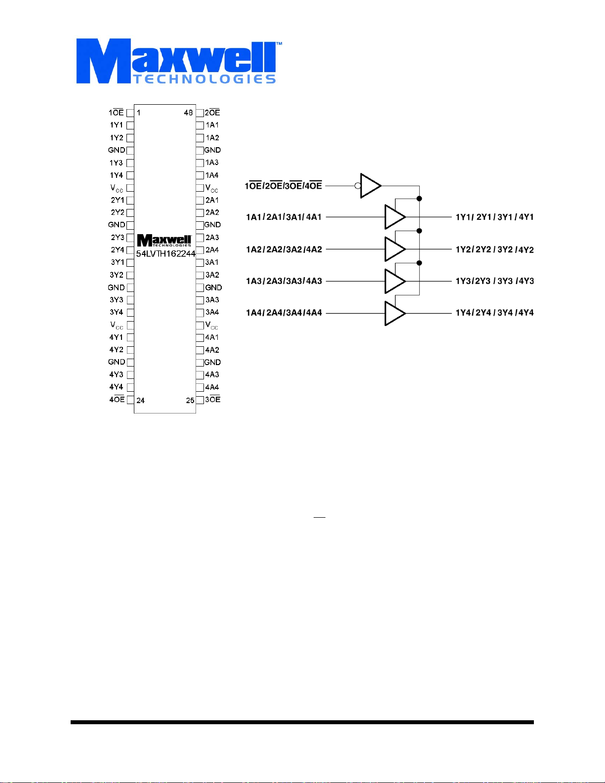
Logic Diagram
DESCRIPTION:
Maxwell Technologies’ 54LVTH162244 devices are 16-bit buffers and line drivers designed for low-voltage (3.3V) V
ation, but with the capability to provide a TTL interface to a 5V
system environment. These devices can be used as four 4-bit
buffers, two 8-bit buffers, or one 16-bit buffer. These devices
provide true outputs and symmetrical active-low output-enable
(OE
) inputs.
The outputs, which are designed to source or sink up to 12
mA, include equivalent 22shoot and undershoot. Active bus-hold circuitry is provided to
hold unused or floating data inputs at a valid logic level.
Maxwell Technologies' patented R
ogy incorporates radiation shielding in the microcircuit package. It eliminates the need for box shielding while providing
the required radiation shielding for a lifetime in orbit or space
mission. In a GEO orbit, R
krad (Si) radiation dose tolerance. This product is available
with screening up to Class S.
Ω series resistors to reduce over-
AD-PAK® packaging technol-
AD-PAK provides greater than 100
CC
oper-
1000607
(858) 503-3300 - Fax: (858) 4503-3301 - www.maxwell.com
12.19.01 Rev 1
All data sheets are subject to change without notice
©2001 Maxwell Technologies.
All rights reserved.
1
Page 2
16-Bit Buffers/Drivers with 3-State Outputs
TABLE 1. PINOUT DESCRIPTION
PIN SYMBOL DESCRIPTION
1, 48, 25, 24 1OE-4OE Output Enable
2, 3, 5, 6 1Y1-1Y4 Output
4, 10, 15, 21, 28, 34,
39, 45
7, 18, 31, 42 V
8, 9, 11, 12 2Y1-2Y4 Output
13, 14, 16, 17 3Y1-3Y4 Output
19, 20, 22, 23 4Y1-4Y4 Output
47, 46, 44, 43 1A1-1A4 Input
41, 40, 38, 37 2A1-2A4 Input
36, 35, 33, 32 3A1-3A4 Input
30, 29, 27, 26 4A1-4A4 Input
GND Ground
CC
Supply Voltage
54LVTH162244
Memory
TABLE 2. 162244 ABSOLUTE MAXIMUM RATINGS
P
ARAMETER SYMBOL MIN MAX UNIT
Supply Voltage Range V
Input Voltage Range
2
Voltage range applied to any output in the high-impedance or
power-off state
Voltage range applied to any output in the high state
2
2
Current into any output in the low state I
Current into any output in the high state
3
Input clamp current I
Output clamp current I
Operating Temperature T
Storage Temperature Range T
Operating Temperature Range T
CC
V
I
V
O
V
O
O
I
O
(VI < 0) -- -50 mA
IK
(VO < 0) -- -50 mA
OK
A
S
A
1
-0.5 4.6 V
-0.5 7 V
-0.5 7 V
-0.5 to V
CC
0.5 V
-- 30 mA
30 -- mA
-55 125 °C
-65 150
-55 125 °C
°
C
1. Stresses beyond listed under “absolute maximum ratings” may cause permanent damage to the device. These are stress ratings only and functional operation of the device at these or any other conditions beyond those indicated under “recommended
operating conditions” is not implied. Exposure to absolute-maximum-rated conditions for extended periods may affect device
reliability.
2. The input and output negative-voltage ratings may be exceeded if the input and output clamp-current ratings are observed.
3. This current flows only when the output is in the high state and VO > VCC.
1000607
12.19.01 Rev 1
All data sheets are subject to change without notice
©2001 Maxwell Technologies.
All rights reserved.
2
Page 3
16-Bit Buffers/Drivers with 3-State Outputs
TABLE 3. DELTA LIMITS
PARAMETER VARIATION
54LVTH162244
I
CC(OP)
I
OZH
I
OZL
TABLE 4. 162244 RECOMMENDED OPERATING CONDITIONS
ARAMETER SYMBOL MIN MAX UNIT
P
Supply Voltage V
High-level Input Voltage V
Low-level Input Voltage V
Input Voltage V
High-level output current I
Low-level output current I
Input Transition Rise or Fall Rate Outputs
±10% of specified value on Table 5
±10% of specified value on Table 5
±10% of specified value on Table 5
CC
IH
IL
I
OH
OL
2.7 3.6 V
2--V
-- 0.8 V
-- 5.5 V
-- -12 mA
-- 12 mA
∆t/∆v-- 10 ns/V
1
enabled
Power-up ramp rate
∆t/∆V
Operating Temperature T
CC
A
200 -- µs/V
-55 125
1. All unused control inputs of the device must be held at high or low to ensure proper device operation.
Memory
°
C
P
ARAMETER SYMBOL TEST CONDITIONS MIN MAX UNIT
Input Clamp Voltage V
High-Level Output Voltage V
Low-Level Output Voltage V
Input Current I
Hold Current I
Output Disabled Leakage
Current - High
1000607
TABLE 5. 162244 DC ELECTRICAL CHARACTERISTICS
(VCC = 3.3V ±10%, TA = -55 TO +125°C, UNLESS OTHERWISE SPECIFIED)
VCC = 2.7 II = -18mA -- -1.2 V
IK
OHVCC
OL
I
I(HOLD)VCC
I
OZHVCC
= 3V IOH = -12 mA 2 -- V
VCC = 3V IOL = 12 mA -- 0.8 V
VCC = 0 or 3.6V VI = 5.5V -- 10 µA
V
= 3.6V VI = VCC or
CC
Control inputs -- ±1
GND
V
= 3.6V VI = V
CC
CC
V
= 0 -- -5
I
Data Inputs -- 1
= 3V VI = 0.8V Data Inputs 75 -- µA
V
= 2V -75 --
I
= 3.6V, VO = 3V -- 5 µA
12.19.01 Rev 1
All data sheets are subject to change without notice
3
©2001 Maxwell Technologies.
All rights reserved.
Page 4

16-Bit Buffers/Drivers with 3-State Outputs
TABLE 5. 162244 DC ELECTRICAL CHARACTERISTICS
(VCC = 3.3V ±10%, TA = -55 TO +125°C, UNLESS OTHERWISE SPECIFIED)
P
ARAMETER SYMBOL TEST CONDITIONS MIN MAX UNIT
54LVTH162244
Output Disabled Leakage
I
OZLVCC
= 3.6V, VO = 0.5V -- -5 µA
Current - Low
Power Up Current I
Power Down Current I
Supply Current I
Delta Supply Current
Input Capacitance C
Input Output Capacitance C
OZPU
OZPD
∆I
2
VCC = 0 to 1.5V, VO = 0.5V to 3V, OE = don’t care -- ±100 µA
2
VCC = 1.5V to 0, VO = 0.5V to 3V, OE = don’t care -- ±100 µA
VCC = 3.6V Outputs high -- 0.19 mA
CC
I
= 0 Outputs low -- 5
O
V
= VCC or GND Outputs disabled -- 0.19
I
1
V
CC
I
O
2
2
= 3V to 3.6V, One input at VCC -0.6V, Other inputs
CC
at V
or GND
CC
VI = 3V or 0 -- 8 pF
VO = 3V or 0 -- 15 pF
-- 0.2 mA
1. This is the increase in supply current for each input that is at the specified TTL voltage level rather than V
2. Guaranteed by design.
TABLE 6. 162244 AC ELECTRICAL CHARACTERISTICS
(TA = -55 TO +125°C, CL = 50 PF, UNLESS OTHERWISE SPECIFIED)
P
ARAMETER SYMBOL
VCC = 3.3V ±V VCC = 2.7V
or GND.
CC
Memory
U
NIT
Propogation Delay Time
A to Y
Output Enable Time
OE
to Y
Output Disable Time
OE
to Y
Output Skew t
1000607
t
PLH
t
PHL
t
PZH
t
PZL
t
PHZ
t
PLZ
sk(o)
MIN MAX MIN MAX
1.1 4.6 -- 5.1 ns
1.1 3.9 -- 4.5
1.1 5.4 -- 6.7 ns
1.3 4.9 -- 6.1
1.6 5.9 -- 6.5 ns
15.9--5.8
-- -- -- -- ns
12.19.01 Rev 1
All data sheets are subject to change without notice
4
©2001 Maxwell Technologies.
All rights reserved.
Page 5

16-Bit Buffers/Drivers with 3-State Outputs
TABLE 7. FUNCTION TABLE
(EACH 4-BIT BUFFER)
INPUTS OUTPUT
OE
AY
LHH
LLL
HXZ
FIGURE 1. LOAD CIRCUIT FOR OUTPUTS
54LVTH162244
Memory
Figure Note:
1. C
includes probe and jog capacitance
L
.
PARAMETER MEASUREMENT INFORMATION
TEST S1
t
PLH/tPHL
t
PLZ/tPZL
t
PHZ/tPZH
Open
6V
GND
FIGURE 2. PULSE DURATION
1000607
12.19.01 Rev 1
All data sheets are subject to change without notice
©2001 Maxwell Technologies.
All rights reserved.
5
Page 6

16-Bit Buffers/Drivers with 3-State Outputs
FIGURE 3. SETUP AND HOLD TIMES
FIGURE 4. PROPAGATION DELAY TIMES INVERTING AND NON-INVERTING OUTPUTS
54LVTH162244
Memory
FIGURE 5. OUTPUT ENABLE TIMING
Figure Notes:
2. All input pulses are supplied by generators having the following characteristics: PRR <
ns.
3. Waveform 1 is for an output with internal conditions such that the output is low except when disabled by the output control.
Waveform 2 is for an output with internal conditions such that the output is high except when disabled by the output control.
4. The outputs are measured one at a time with one transition per measurement.
10 MHz, Z
= 50 Ω, t
O
< 2.5 ns, tf < 2.5
r
1000607
12.19.01 Rev 1
All data sheets are subject to change without notice
©2001 Maxwell Technologies.
All rights reserved.
6
Page 7

16-Bit Buffers/Drivers with 3-State Outputs
54LVTH162244
Memory
48 PIN RAD-PAK® FLAT PACKAGE
SYMBOL DIMENSION
MIN NOM MAX
A 0.121 0.130 0.139
b 0.008 0.010 0.014
c 0.004 0.006 0.006
D -- 0.620 0.640
E 0.370 0.380 0.390
E1 -- -- 0.410
E2 0.200 0.210 0.220
E3 0.075 0.085 --
e 0.025 BSC
L 0.275 0.285 0.295
Q 0.000 0.019 0.045
S1 0.005 0.018 --
N48
F48-01
Note: All dimensions in inches
1000607
12.19.01 Rev 1
All data sheets are subject to change without notice
©2001 Maxwell Technologies.
All rights reserved.
7
Page 8

16-Bit Buffers/Drivers with 3-State Outputs
Important Notice:
These data sheets are created using the chip manufacturer’s published specifications. Maxwell Technologies verifies
functionality by testing key parameters either by 100% testing, sample testing or characterization.
The specifications presented within these data sheets represent the latest and most accurate information available to
date. However, these specifications are subject to change without notice and Maxwell Technologies assumes no
responsibility for the use of this information.
Maxwell Technologies’ products are not authorized for use as critical components in life support devices or systems
without express written approval from Maxwell Technologies.
Any claim against Maxwell Technologies must be made within 90 days from the date of shipment from Maxwell Technologies. Maxwell Technologies’ liability shall be limited to replacement of defective parts.
54LVTH162244
Memory
1000607
12.19.01 Rev 1
All data sheets are subject to change without notice
©2001 Maxwell Technologies.
All rights reserved.
8
Page 9

16-Bit Buffers/Drivers with 3-State Outputs
)
Product Ordering Options
Model Number
54LVTH162244
54LVTH162244
RP
F X
Feature
Screening Flow
Package
Option Details
Monolithic
S = Maxwell Class S
B = Maxwell Class B
E = Engineering (testing @ +25°C
I = Industrial (testing @ -55°C,
+25°C, +125°C)
F = Flat Pack
Memory
1000607
Radiation Feature
Base Product
Nomenclature
12.19.01 Rev 1
RP = R
AD-PAK® package
16-Bit Buffers/Drivers with 3-State
Outputs
All data sheets are subject to change without notice
©2001 Maxwell Technologies.
All rights reserved.
9
 Loading...