

Datasheet 54RHSCT630CC, 54RHSCT630CB, 54QHSCT630FS, 54QHSCT630FL, 54QHSCT630FE Datasheet (DYNEX)
...Page 1
54HSC/T630
1/10
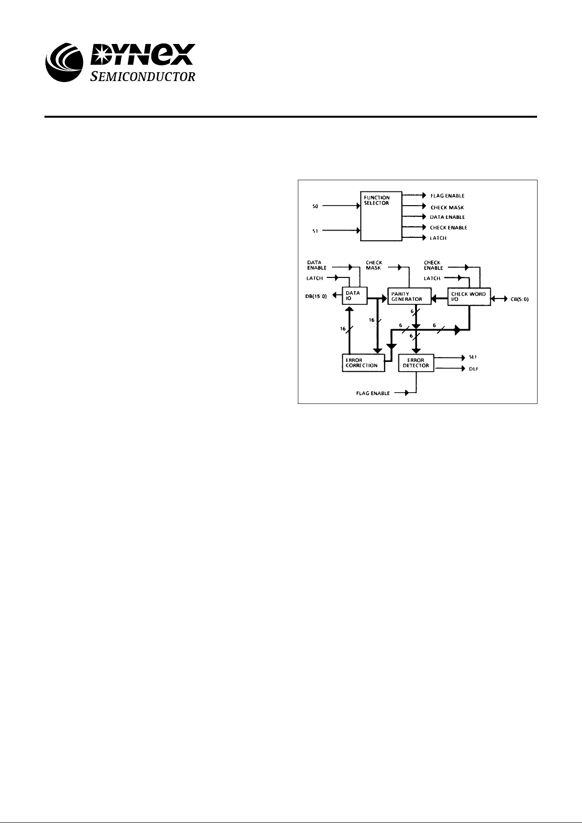
The 54HSC/T630 is a 16-bit parallel Error Detection and
Correction circuit. It uses a modified Hamming code to
generate a 6-bit check word from each 16-bit data word. The
check word is stored with the data word during a memory write
cycle. During a memory read cycle a 22-bit word is taken from
memory and checked for errors.
Single bit errors in data words are flagged and corrected.
Single bit errors in check words are flagged but not corrected.
The position of the incorrect bit is pinpointed, in both cases, by
the 6-bit error syndrome code which is output during the error
correction cycle.
Two bit errors are flagged but not corrected. Any
combination of two bit errors occurring within the 22-bit word
read from memory, (ie two errors in the 16-bit data word, two
bits in the 16-bit check word or one error in each) will be
correctly identified.
The gross errors of all bits, low or high, will be detected.
The control signals S1 and S0 select the function to be
performed by the EDAC They control the generation of check
words and the latching and correction of data (see table 1)
When errors are detected, flags are placed on outputs SEF
and DEF (see table 2).
Figure 1: Block Diagram
FEATURES
■ Radiation Hard:
Dose Rate Upset Exceeding 3x10
10
Rad(Si)/sec
Total Dose for Functionality Upto 1x10⁶ Rad(Si)
■ High SEU Immunity, Latch Up Free
■ CMOS-SOS Technology
■ All Inputs and Outputs Fully TTL Compatible (54HST630)
or CMOS Compatible (54HSC630)
■ Low Power
■ Detects and Corrects Single-Bit Errors
■ Detects and Flags Dual-Bit Errors
■ High Speed:
Write Cycle - Generates Checkword In 40ns Typical
Read Cycle - Flags Errors In 20ns Typical
54HSC/T630
Radiation hard 16-Bit ParallelError
Detection & Correction
Replaces June 1999 version, DS3595-4.0 DS3595-5.0 January 2000
Page 2
54HSC/T630
2/10
Table 1: Control Functions
Control Error Flags
Cycle S1 S0 EDAC Function Data UO Checkword SEF DEF
WRITE Low Low Generates Checkword Input Data Output Checkword Low Low
READ Low High Read Data BCheckword Input Data Input Checkword Low Low
READ High High Latch & Flag Error Latch Data Latch Checkword Enabled Enabled
READ High Low Correct Data Word & Output Output Syndrome Bits Enabled Enabled
Generate Syndrome Bits Corrected
Data
Table 2: Error Functions
Total Number of Errors Error Flags Data Correction
16-bit Data 6-bit Checkword SEF DEF
0 0 Low Low Not Applicable
1 0 High Low Correctlon
0 1 High Low Correction
1 1 High High Interrupt
2 0 High High Interrupt
0 2 High High Interrupt
ERROR DETECTION & CORRECTION
During a memory write cycle, six check bits (CBO-CB5)
are generated by eight-input parity generators using the data
bits defined in Table 3. During a memory read cycle, the 6-bit
checkword is retrieved along with the actual data.
Error detection is accomplished as the 6-bit checkword and
the 16-bit data word from memory are applied to internal parity
generators/checkers. If the parity of all six groupings of data
and check bits are correct, it is assumed that no error has
occurred and both error flags will be low. It should be noted
that the sense of two of the check bits, bits CBO and CB1, is
inverted to ensure that the gross-error condition of all lows and
all highs is detected.
If the parity of one or more of the check groups is incorrect,
an error has occurred and the proper error flag or flags will be
set high. Any single error in the 16bit data word will change the
sense of exactly three bits of the 6-bit checkword. Any single
error in the 6bit checkword changes the sense of only that one
bit. In either case, the single error flag will be set high while the
dual error flag will remain low.
Any two-bit error will change the sense of an even number
of check bits. The two-bit error is not correctable since the
parity tree can only identify singlebit errors. Both error flags are
set high when any two-bit error is detected.
Three or more simultaneous bit errors cause the EDAC to
transmit that no error, a correctable error, or an uncorrectable
error has occurred and hence produce erroneous results in all
three cases.
Error correction is accomplished by identifying the bad bit
and inverting it. Identification of the erroneous bit is achieved
by comparing the 16-bit word and 6-bit checkword from
memory with the new checkword with one (checkword error)
or three (data word error) inverted bits.
As the corrected word is made available on the data word l/
O port, the checkword l/O port presents a 6-bit syndrome error
code. This syndrome code can be used to identify the
corrupted bit in memory (see Table 4. overleaf).
Page 3
54HSC/T630
3/10
14
X
X
X
13
X
X
X
12
X
X
X
11
X
X
X
10
X
X
X
9
X
X
X
8
X
X
X
16-bit Data Word
Checkword
Bit
CB0
CB1
CB2
CB3
CB4
CB5
2
X
X
X
15
X
X
X
7
X
X
X
6
X
X
X
5
X
X
X
4
X
X
X
1
X
X
X
3
X
X
X
0
X
X
X
The six check bits are partly bits derived from the matrix of data bits as indicated by 'X' for each bit.
Table 3: Check Word Generation
Error Location
DB15
H
H
L
H
L
L
CB0
L
H
H
H
H
H
CB1
H
L
H
H
H
H
CB2
H
H
L
H
H
H
CB3
H
H
H
L
H
H
CB4
H
H
H
H
L
H
CB5
H
H
H
H
H
L
No
Error
H
H
H
H
H
H
DB0
L
L
H
L
H
H
DB1
L
H
L
L
H
H
DB2
H
L
L
L
H
H
DB3
L
L
H
H
L
H
DB4
L
H
L
H
L
H
DB5
H
L
L
H
L
H
DB6
H
L
H
L
L
H
DB7
H
H
L
L
L
H
DB8
L
L
H
H
H
L
DB9
L
H
L
H
H
L
DB10
L
H
H
L
H
L
DB11
H
L
H
L
H
L
DB12
H
H
L
L
H
L
DB13
L
H
H
H
L
L
DB14
H
L
H
H
L
L
Syndrome
Error
Code
CB0
CB1
CB2
CB3
CB4
CB5
Table 4: Error Syndrome Codes
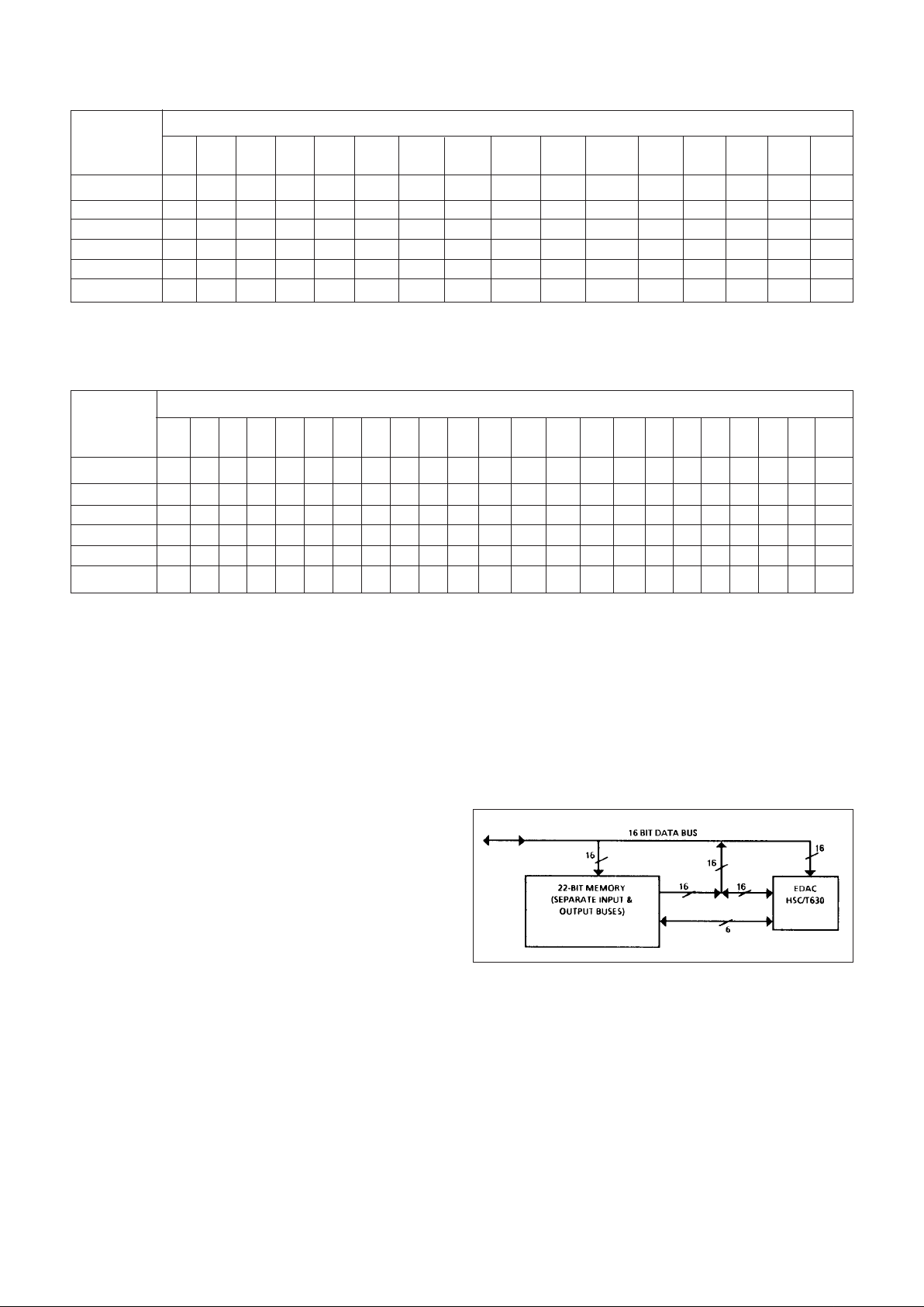
APPLICATIONS
Although many semiconductor memories have separate
input and output pins, it is possible to design the error
detection and correction function using a single EDAC. EDAC
data and check bit pins function as inputs or outputs
dependent upon the state of control signals S0 and S1. It
becomes necessary to use wired AND logic, with fairly
complex timing system, to control the EDAC and data bus.
This scheme becomes difficult to implement both in terms of
board layout and timing. System performance is also
adversely affected, See Figure 2.
Optimised systems can be implemented using two EDAC’s
in parallel, One of the units is used strictly as an encoder
during the memory write cycle. Both controls S0 and Sl are
grounded, The encoder chip will generate the 6-bit check word
for memory storage along with the 16-bit data.
The second of the two EDAC’s will be used as a decoder
during the memory read cycle. This decoder chip requires
timing pulses for correct operation. Control S1 is set low and
S0 high as the memory read cycle begins. After the memory
output data is valid, the control S1 input is moved from the low
to a high. This low-to-high transition latches the 22-bit word
from memory into internal registers of this second EDAC and
enables the two error flags. If no error occurs, the CPU can
accept the 16-bit word directly from memory. If a single error
has occurred, the CPU must move the control SO input from
the high to a low to output corrected data and the error
syndrome bits. Any dual error should be an interrupt condition.
In most applications, status registers will be used to keep
tabs on error flags and error syndrome bits. If repeated
patterns of error flags and syndrome bits occur, the CPU will
be able to recognize these symptoms as a “hard” error. The
syndrome bits can be used to pinpoint the faulty memory chip,
See Figure 3.
Figure 2: Error Detection and Correction Using a
Single EDAC Unit
Page 4

54HSC/T630
4/10
Figure 3: Error Detection and Correction Using Two EDAC Units
S1 S0 Function
L H Start READ
H H Latch data & flag errors
H L Correct data & Output syndrome bits
DC CHARACTERISTICS AND RATINGS
Parameter Min Max Units
Supply Voltage -0.5 7 V
Input Voltage V
SS
-0.3 VDD+0.3 V
Current Through Any Pin -20 +20 mA
Operating Temperature -55 125 °C
Storage Temperature -65 150 °C
Note: Stresses above those listed may cause permanent
damage to the device. This is a stress rating only and
functional operation of the device at these conditions, or at
any other condition above those indicated in the operations
section of this specification, is not implied. Exposure to
absolute maximum rating conditions for extended periods
may affect device reliability.
Table 5: Absolute Maximum Ratings
Subgroup Definition
1 Static characteristics specified in Table 6 at +25°C
2 Static characteristics specified in Table 6 at +125°C
3 Static characteristics specified in Table 6 at -55°C
9 Switching characteristics specified in Table 7 at +25°C
10 Switching characteristics specified in Table 7 at +125°C
11 Switching characteristics specified in Table 7 at -55°C
DEFINITION OF SUBGROUPS
Page 5

54HSC/T630
5/10
Total dose radiation not
exceeding 3x10⁵ Rad(SI)
Symbol Parameter Conditions Min Typ Max Units
V
DD
Supply Voltage - 4.5 5.0 5.5 V
V
IH1
TTL Input High Voltage - 2.0 - - V
V
IL1
TTL Input Low Voltage - - - 0.8 V
V
IH2
CMOS Input High Voltage - 3.5 - - V
V
IL2
CMOS Input Low Voltage - - - 1.5 V
V
OH1
TTL Output High Voltage IOH = -4mA 2.4 - - V
V
OL1
TTL Output Low Voltage IOL = 12mA (CB or DB), - - 0.4 V
IOL = 4mA (SEF or DEF)
V
OH2
CMOS Output High Voltage IOH = -4mA VDD-0.5 - - V
V
OL2
CMOS Output Low Voltage IOL = 12mA (CB or DB), - - 0.5 V
I
OL
= 4mA (SEF or DEF)
I
1L
Input Low Current VDD = 5.5, VIN = V
SS
- - -10 µA
I
1H
Input High Current VDD = 5.5, VIN = V
DD
--50µA
I2LIO Low Current VDD = 5.5, VIN = V
SS
- - -50 µA
I
2H
IO High Current VDD = 5.5, VIN = V
DD
--50µA
IDDPower Supply Current VDD = Max, S0 & S1 at - - 1 mA
5.5V, All CB & DB pins
grounded, DEF & SEF
open
VDD = 5V±10%, over full operating temperature range.
Mil-Std-883, method 5005, subgroups 1, 2, 3
Parameters at higher radiation levels available on request.
Table 6: Electrical Characteristics
Parameter
t
PLH
Propogation delay time, low-to-high-level output (Note 4)
t
PLH
Propogation delay time, low-to-high-level output (Note 4)
t
PLH
Propogation delay time, low-to-high-level output (Note 5)
t
PLH
Propogation delay time, low-to-high-level output (Note 5)
t
PZH
Output enable time to high level (Note 6)
t
PZL
Output enable time to low level (Note 6)
t
PHZ
Output disable time to high level (Note 7)
t
PLZ
Output disable time to low level (Note 7)
tS Set-up time to S1 ›
tH Hold time after S1 ›
1. VDD = 5V ±10% and CL = 50pF, over full operating temperature and total dose = 300K Rad(Si)
2. Input Pulse VSS to 3.0 Volts.(TTL), VDD -1V (CMOS).
3. Times Measurement Reference Level 1.5 Volts.
4. These parameters describe the time intervals taken to generate the check word during the memory write cycle.
5. These parameters describe the time intervals taken to flag errors during memory read cycle.
6. These parameters describe the time intervals taken to correct and output the data word and to generate and output the syndrome error code during
the memory read cycle.
7. These parameters describe the time intervals taken to disable the CB & DB buses in preparation for a new data word during the memory read cycle.
8. Mil-Std-883, method 5005, subgroups 9, 10, 11
9.
Parameters at higher radiation levels available on request.
From
(Input)
DB
DB
S1 ⇑
S1 ⇑
S0 ⇓
S0 ⇓
S0 ⇑
S0 ⇑
CB, DB
CB, DB
To
(Output)
CB
CB
DEF
SEF
CB, DB
CB, DB
CB, DB
CB, DB
-
-
Min.
-
-
-
-
-
-
-
30
15
Max.
58
58
29
29
40
45
45
65
-
-
Units
ns
ns
ns
ns
ns
ns
ns
ns
ns
ns
Conditions (HST)
S0 = 0V, S1 = 0V
S0 = 0V, S1 = 0V
S0 = 3V
S0 = 3V
S1 = 3V (fig. 5)
S1 = 3V (fig. 4)
S1 = 3V (fig. 5)
S1 = 3V (fig. 4)
-
-
Conditions (HSC)
S0 = 0V, S1 = 0V
S0 = 0V, S1 = 0V
S0 = V
DD
-1V
S0 = VDD-1V
S1 = VDD-1V (fig. 5)
S1 = VDD-1V (fig. 4)
S1 = VDD-1V (fig. 5)
S1 = V
DD
-1V (fig. 4)
-
-
AC ELECTRICAL CHARACTERISTICS
Table 7: AC Electrical Characteristics
Page 6

54HSC/T630
6/10
Figure 4: Output Load Circuit Figure 5: Output Load Circuit
Figure 6: Read, Flag and Correct, Made Switching Waveforms
(Note 6)
(Note 6)
(Note 5)
(Note 5)
(Note 7)
(Note 7)
t
s
Page 7

54HSC/T630
7/10
PIN ASSIGNMENTS
Figure 7: 28-Lead Ceramic DIL (Solder Seal)
- Package Style C
Figure 8: 28-Lead Flatpack (Solder Seal) - Package Style F
PACKAGE OUTLINES
Figure 9: 28-Lead Ceramic DIL (Solder Seal) - Package Style C
D
W
A
e b Z
H
A
1
15°
M
E
C
e
1
Seating Plane
114
2815
Ref
Millimetres Inches
Min. Nom. Max. Min. Nom. Max.
A - - 5.715 - - 0.225
A1 0.38 - 1.53 0.015 - 0.060
b 0.35 - 0.59 0.014 - 0.023
c 0.20 - 0.36 0.008 - 0.014
D - - 36.02 - - 1.418
e - 2.54 Typ. - - 0.100 Typ. -
e1 - 15.24 Typ. - - 0.600 Typ. -
H 4.71 - 5.38 0.185 - 0.212
Me - - 15.90 - - 0.626
Z - - 1.27 - - 0.050
W - - 1.53 - - 0.060
XG404
Page 8

54HSC/T630
8/10
Ref
Millimetres Inches
Min. Nom. Max. Min. Nom. Max.
A - - 2.97 - - 0.117
b 0.38 - 0.48 0.015 - 0.019
c 0.076 - 0.152 0.003 - 0.006
D 18.08 - 18.49 0.712 - 0.728
E 12.50 - 12.90 0.492 - 0.508
E2 9.45 - 9.85 0.372 - 0.388
e 1.14 - 1.40 0.045 - 0.055
L 8.00 - 9.27 0.315 - 0.365
Q 0.66 - - 0.026 - -
S - - 1.14 - - 0.045
XG543
Figure 10: 28-Lead Ceramic Flatpack (Solder Seal) - Package Style F
E
b
e
D
L
A
Q
c
Pin 1
S
E2
Page 9

54HSC/T630
9/10
RADIATION TOLERANCE
Total Dose Radiation Testing
For product procured to guaranteed total dose radiation
levels, each wafer lot will be approved when all sample
devices from each lot pass the total dose radiation test.
The sample devices will be subjected to the total dose
radiation level (Cobalt-60 Source), defined by the ordering
code, and must continue to meet the electrical parameters
specified in the data sheet. Electrical tests, pre and post
irradiation, will be read and recorded.
GEC Plessey Semiconductors can provide radiation
testing compliant with Mil-Std-883 method 1019 Ionizing
Radiation (total dose) test.
ORDERING INFORMATION
For details of reliability, QA/QC, test and assembly
options, see ‘Manufacturing Capability and Quality
Assurance Standards’ Section 9.
Unique Circuit Designator
‘Blank’
R
Q
H *
No tolerance implied
100 kRads (Si) Guaranteed
300 kRads (Si) Guaranteed
1000 kRads (Si) Guaranteed
*HSC Onl
y
Radiation Tolerance
CFCeramic DIL (Solder Seal)
Flatpack (Solder Seal)
Package Type
QA/QCI Process
(See Section 9 Part 4)
Test Process
(See Section 9 Part 3)
Assembly Process
(See Section 9 Part 2)
L
C
D
E
B
S
Rel 0
Rel 1
Rel 2
Rel 3/4/5/STACK
Class B
Class S
Reliability Level
54xHSC/T630xxxxx
Total Dose (Function to specification)* 3x10⁵ Rad(Si)
Transient Upset (Stored data loss) 5x10¹⁰ Rad(Si)/sec
Transient Upset (Survivability) >1x10
12
Rad(Si)/sec
Neutron Hardness (Function to specification) >1x10¹⁵ n/cm
2
Single Event Upset** <1x10
-10
Errors/bit day
Latch Up Not possible
* Other total dose radiation levels available on request
** Worst case galactic cosmic ray upset - interplanetary/high altitude orbit
Figure 11: Radiation Hardness Parameters
Page 10

54HSC/T630
10/10
CUSTOMER SERVICE CENTRES
France, Benelux, Italy and Spain Tel: +33 (0)1 69 18 90 00. Fax: +33 (0)1 64 46 54 50
North America Tel: 011-800-5554-5554. Fax: 011-800-5444-5444
UK, Germany, Scandinavia & Rest Of World Tel: +44 (0)1522 500500. Fax: +44 (0)1522 500020
SALES OFFICES
France, Benelux, Italy and Spain Tel: +33 (0)1 69 18 90 00. Fax: +33 (0)1 64 46 54 50
Germany Tel: 07351 827723
North America Tel: (613) 723-7035. Fax: (613) 723-1518. Toll Free: 1.888.33.DYNEX (39639) /
Tel: (831) 440-1988. Fax: (831) 440-1989 / Tel: (949) 733-3005. Fax: (949) 733-2986.
UK, Germany, Scandinavia & Rest Of World Tel: +44 (0)1522 500500. Fax: +44 (0)1522 500020
These offices are supported by Representatives and Distributors in many countries world-wide.
© Dynex Semiconductor 2000 Publication No. DSxxxx-y Issue No. x.x January 2000
TECHNICAL DOCUMENTATION – NOT FOR RESALE. PRINTED IN UNITED KINGDOM
HEADQUARTERS OPERATIONS
DYNEX SEMICONDUCTOR LTD
Doddington Road, Lincoln.
Lincolnshire. LN6 3LF. United Kingdom.
Tel: 00-44-(0)1522-500500
Fax: 00-44-(0)1522-500550
DYNEX POWER INC.
Unit 7 - 58 Antares Drive,
Nepean, Ontario, Canada K2E 7W6.
Tel: 613.723.7035
Fax: 613.723.1518
Toll Free: 1.888.33.DYNEX (39639)
This publication is issued to provide information only which (unless agreed by the Company in writing) may not be used, applied or reproduced for any purpose nor form part of any order or contract nor to be regarded
as a representation relating to the products or services concerned. No warranty or guarantee express or implied is made regarding the capability, performance or suitability of any product or service. The Company
reserves the right to alter without prior notice the specification, design or price of any product or service. Information concerning possible methods of use is provided as a guide only and does not constitute any
guarantee that such methods of use will be satisfactory in a specific piece of equipment. It is the user's responsibility to fully determine the performance and suitability of any equipment using such information and
to ensure that any publication or data used is up to date and has not been superseded. These products are not suitable for use in any medical products whose failure to perform may result in significant injury
or death to the user. All products and materials are sold and services provided subject to the Company's conditions of sale, which are available on request.
All brand names and product names used in this publication are trademarks, registered trademarks or trade names of their respective owners.
http://www.dynexsemi.com
e-mail: power_solutions@dynexsemi.com
Datasheet Annotations:
Dynex Semiconductor annotate datasheets in the top right hard corner of the front page, to indicate product status. The annotations are as follows:-
Target Information: This is the most tentative form of information and represents a very preliminary specification. No actual design work on the product has been started.
Preliminary Information: The product is in design and development. The datasheet represents the product as it is understood but details may change.
Advance Information: The product design is complete and final characterisation for volume production is well in hand.
No Annotation: The product parameters are fixed and the product is available to datasheet specification.
 Loading...