

Page 1
TL/F/9556
54F/74F545 Octal Bidirectional Transceiver with TRI-STATE Outputs
May 1995
54F/74F545 Octal Bidirectional
Transceiver with TRI-STATE
É
Outputs
General Description
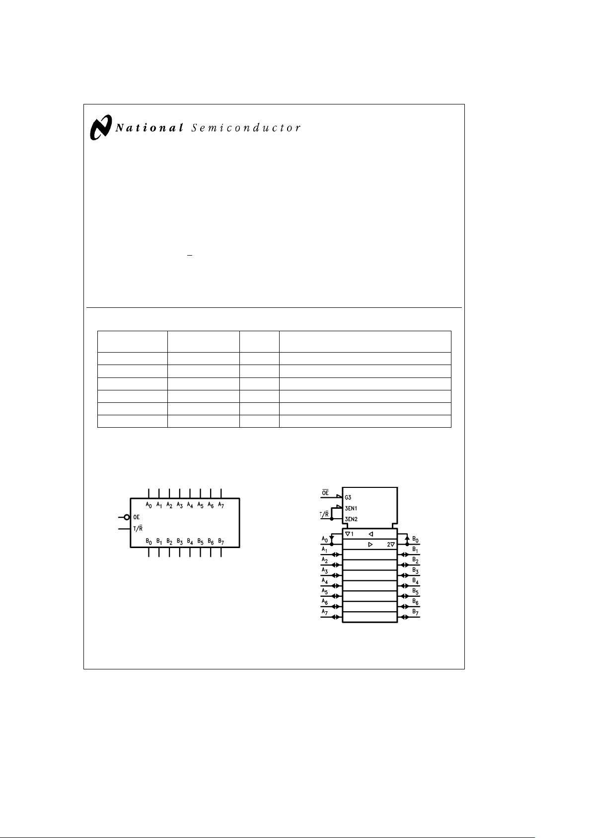
The ’F545 is an 8-bit, TRI-STATE, high-speed transceiver. It
provides bidirectional drive for bus-oriented microprocessor
and digital communications systems. Straight through bidirectional transceivers are featured, with 24 mA (20 mA Mil)
bus drive capability on the A ports and 64 mA (48 mA Mil)
bus drive capability on the B ports.
One input, Transmit/Receive (T/R
) determines the direction
of logic signals through the bidirectional transceiver. Transmit enables data from A ports to B ports; Receive enables
data from B ports to A ports. The Output Enable input disables both A and B ports by placing them in a TRI-STATE
condition.
Features
Y
Higher drive than 8304
Y
8-bit bidirectional data flow reduces system package
count
Y
TRI-STATE inputs/outputs for interfacing with bus-oriented systems
Y
24 mA (20 mA Mil) and 64 mA (48 mA Mil) bus drive
capability on A and B ports, respectively
Y
Transmit/Receive and Output Enable simplify control
logic
Y
Guaranteed 4000V minimum ESD protection
Y
Pin for Pin compatible with Intel 8286
Commercial Military
Package
Package Description
Number
74F545PC N20A 20-Lead (0.300×Wide) Molded Dual-In-Line
54F545DM (Note 2) J20A 20-Lead Ceramic Dual-In-Line
74F545SC (Note 1) M20B 20-Lead (0.300×Wide) Molded Small Outline, JEDEC
74F545SJ (Note 1) M20D 20-Lead (0.300×Wide) Molded Small Outline, EIAJ
54F545FM (Note 2) W20A 20-Lead Cerpack
54F545LM (Note 2) E20A 20-Lead Ceramic Leadless Chip Carrier, Type C
Note 1: Devices also available in 13×reel. Use suffixeSCX and SJX.
Note 2: Military grade device with environmental and burn-in processing. Use suffix
e
DMQB, FMQB and LMQB.
Logic Symbols
TL/F/9556– 3
IEEE/IEC
TL/F/9556– 5
TRI-STATEÉis a registered trademark of National Semiconductor Corporation.
C
1995 National Semiconductor Corporation RRD-B30M105/Printed in U. S. A.
Page 2
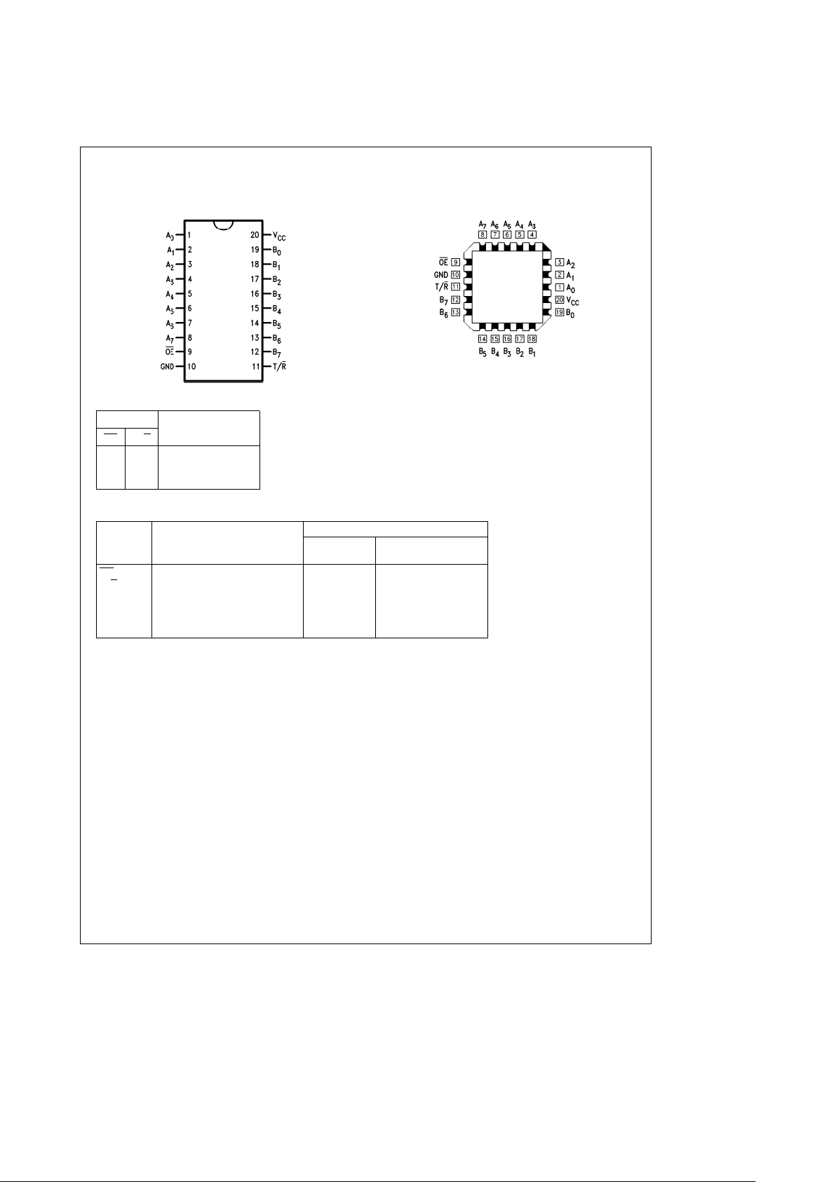
Connection Diagrams
Pin Assignment for
DIP, SOIC and Flatpak
TL/F/9556– 1
Pin Assignment
for LCC
TL/F/9556– 2
Truth Table
Inputs
Outputs
OE T/R
L L Bus B Data to Bus A
L H Bus A Data to Bus B
H X High Z
HeHIGH Voltage Level
L
e
LOW Voltage Level
X
e
Immaterial
Z
e
High Impedance
Unit Loading/Fan Out
54F/74F
Pin Names Description
U.L. Input I
IH/IIL
HIGH/LOW Output IOH/I
OL
OE Output Enable Input (Active LOW) 1.0/2.0 20 mA/b1.2 mA
T/R
Transmit/Receive Input 1.0/2.0 20 mA/b1.2 mA
A
0–A7
Side A TRI-STATE Inputs or 3.5/1.083 70 mA/b650 mA
TRI-STATE Outputs 150/40 (33.3)
b
3 mA/24 mA (20 mA)
B0–B
7
Side B TRI-STATE Inputs or 3.5/1.083 70 mA/b650 mA
TRI-STATE Outputs 600/106.6 (80)
b
12 mA/64 mA (48 mA)
2
Page 3
Absolute Maximum Ratings (Note 1)
If Military/Aerospace specified devices are required,
please contact the National Semiconductor Sales
Office/Distributors for availability and specifications.
Storage Temperature
b
65§Ctoa150§C
Ambient Temperature under Bias
b
55§Ctoa125§C
Junction Temperature under Bias
b
55§Ctoa175§C
Plastic
b
55§Ctoa150§C
V
CC
Pin Potential to
Ground Pin
b
0.5V toa7.0V
Input Voltage (Note 2)
b
0.5V toa7.0V
Input Current (Note 2)
b
30 mA toa5.0 mA
Voltage Applied to Output
in HIGH State (with V
CC
e
0V)
Standard Output
b
0.5V to V
CC
TRI-STATE Output
b
0.5V toa5.5V
Current Applied to Output
in LOW State (Max) twice the rated I
OL
(mA)
ESD Last Passing Voltage (Min) 4000V
Note 1: Absolute maximum ratings are values beyond which the device may
be damaged or have its useful life impaired. Functional operation under
these conditions is not implied.
Note 2: Either voltage limit or current limit is sufficient to protect inputs.
Recommended Operating
Conditions
Free Air Ambient Temperature
Military
b
55§Ctoa125§C
Commercial 0
§
Ctoa70§C
Supply Voltage
Military
a
4.5V toa5.5V
Commercial
a
4.5V toa5.5V
DC Electrical Characteristics
Symbol Parameter
54F/74F
Units V
CC
Conditions
Min Typ Max
V
IH
Input HIGH Voltage 2.0 V Recognized as a HIGH Signal
V
IL
Input LOW Voltage 0.8 V Recognized as a LOW Signal
V
CD
Input Clamp Diode Voltage
b
1.2 V Min I
IN
eb
18 mA (OE, T/R)
V
OH
Output HIGH 54F 10% V
CC
2.5 I
OH
eb
1mA(An)
Voltage 54F 10% V
CC
2.4 I
OH
eb
3mA(An)
54F 10% V
CC
2.0 I
OH
eb
12 mA (Bn)
74F 10% V
CC
2.5
V Min
I
OH
eb
1mA(An)
74F 10% V
CC
2.4 I
OH
eb
3mA(An)
74F 10% V
CC
2.0 I
OH
eb
15 mA (Bn)
74F 5% V
CC
2.7 I
OH
eb
1mA(An)
74F 5% V
CC
2.7 I
OH
eb
3mA(An)
V
OL
Output LOW 54F 10% V
CC
0.5 I
OL
e
20 mA (An)
Voltage 54F 10% V
CC
0.55
V Min
I
OL
e
48 mA (Bn)
74F 10% V
CC
0.5 I
OL
e
24 mA (An)
74F 10% V
CC
0.55 I
OL
e
64 mA (Bn)
I
IH
Input HIGH 54F 20.0
mA Max
V
IN
e
2.7V (OE, T/R)
Current 74F 5.0
I
BVI
Input HIGH Current 54F 100
mA Max
V
IN
e
7.0V (OE, T/R)
Breakdown Test 74F 7.0
I
BVIT
Input HIGH Current 54F 1.0
mA Max
V
IN
e
5.5V (An,Bn)
Breakdown (I/O) 74F 0.5
I
CEX
Output HIGH 54F 250
mA Max
V
OUT
e
V
CC
Leakage Current 74F 50
V
ID
Input Leakage
74F 4.75 V 0.0
I
ID
e
1.9 mA
Test All Other Pins Grounded
I
OD
Output Leakage
74F 3.75 m A 0.0
V
IOD
e
150 mV
Circuit Current All Other Pins Grounded
I
IL
Input LOW Current
b
1.2 mA Max V
IN
e
0.5V (OE, T/R)
I
IH
a
I
OZH
Output Leakage Current 70 mA Max V
OUT
e
2.7V (An,Bn)
I
IL
a
I
OZL
Output Leakage Current
b
650 mA Max V
OUT
e
0.5V (An,Bn)
I
OS
Output Short-Circuit Current
b
60
b
150
mA Max
V
OUT
e
0V (An)
b
100
b
225 V
OUT
e
0V (Bn)
3
Page 4

DC Electrical Characteristics (Continued)
Symbol Parameter
54F/74F
Units V
CC
Conditions
Min Typ Max
I
ZZ
Bus Drainage Test 500 mA 0.0V V
OUT
e
5.25V
I
CCH
Power Supply Current 70 90 mA Max V
O
e
HIGH
I
CCL
Power Supply Current 95 120 mA Max V
O
e
LOW
I
CCZ
Power Supply Current 85 110 mA Max V
O
e
HIGH Z
AC Electrical Characteristics
74F 54F 74F
T
A
ea
25§C
T
A,VCC
e
Mil TA,V
CC
e
Com
Symbol Parameter V
CC
ea
5.0V
C
L
e
50 pF C
L
e
50 pF
Units
C
L
e
50 pF
Min Typ Max Min Max Min Max
t
PLH
Propagation Delay 2.5 4.2 6.0 2.0 7.5 2.5 7.0
ns
t
PHL
Anto Bnor Bnto A
n
2.5 4.6 6.0 2.0 7.5 2.5 7.0
t
PZH
Output Enable Time 3.0 5.3 7.0 2.5 9.0 3.0 8.0
t
PZL
3.5 6.0 8.0 3.0 10.0 3.5 9.0
ns
t
PHZ
Output Disable Time 3.0 5.0 6.5 2.5 9.0 3.0 7.5
t
PLZ
2.0 5.0 6.5 2.0 10.0 2.0 7.5
Logic Diagram
TL/F/9556– 4
Please note that this diagram is provided only for the understanding of logic operations and should not be used to estimate propagation delays.
Ordering Information
The device number is used to form part of a simplified purchasing code where the package type and temperature range are
defined as follows:
74F 545 S C X
Temperature Range Family Special Variations
74F
e
Commercial QBeMilitary grade device with
54F
e
Military environmental and burn-in
processing
Device Type
X
e
Devices shipped in 13×reel
Package Code
Temperature Range
P
e
Plastic DIP
C
e
Commercial (0§Ctoa70§C)
D
e
Ceramic DIP
M
e
Military (b55§Ctoa125§C)
F
e
Flatpak
L
e
Leadless Chip Carrier (LCC)
S
e
Small Outline SOIC JEDEC
SJ
e
Small Outline SOIC EIAJ
4
Page 5

Physical Dimensions inches (millimeters)
20-Lead Ceramic Leadless Chip Carrier (L)
NS Package Number E20A
20-Lead Ceramic Dual-In-Line Package (D)
NS Package Number J20A
5
Page 6

Physical Dimensions inches (millimeters) (Continued)
20-Lead (0.300×Wide) Molded Small Outline Package, JEDEC (S)
NS Package Number M20B
20-Lead (0.300×Wide) Molded Small Outline Package, EIAJ
NS Package Number M20D
6
Page 7

Physical Dimensions inches (millimeters) (Continued)
20-Lead (0.300×Wide) Molded Dual-In-Line Package (P)
NS Package Number N20A
7
Page 8

54F/74F545 Octal Bidirectional Transceiver with TRI-STATE Outputs
Physical Dimensions inches (millimeters) (Continued)
20-Lead Ceramic Flatpak (F)
NS Package Number W20A
LIFE SUPPORT POLICY
NATIONAL’S PRODUCTS ARE NOT AUTHORIZED FOR USE AS CRITICAL COMPONENTS IN LIFE SUPPORT
DEVICES OR SYSTEMS WITHOUT THE EXPRESS WRITTEN APPROVAL OF THE PRESIDENT OF NATIONAL
SEMICONDUCTOR CORPORATION. As used herein:
1. Life support devices or systems are devices or 2. A critical component is any component of a life
systems which, (a) are intended for surgical implant support device or system whose failure to perform can
into the body, or (b) support or sustain life, and whose be reasonably expected to cause the failure of the life
failure to perform, when properly used in accordance support device or system, or to affect its safety or
with instructions for use provided in the labeling, can effectiveness.
be reasonably expected to result in a significant injury
to the user.
National Semiconductor National Semiconductor National Semiconductor National Semiconductor
Corporation Europe Hong Kong Ltd. Japan Ltd.
1111 West Bardin Road Fax: (
a
49) 0-180-530 85 86 13th Floor, Straight Block, Tel: 81-043-299-2309
Arlington, TX 76017 Email: cnjwge@tevm2.nsc.com Ocean Centre, 5 Canton Rd. Fax: 81-043-299-2408
Tel: 1(800) 272-9959 Deutsch Tel: (
a
49) 0-180-530 85 85 Tsimshatsui, Kowloon
Fax: 1(800) 737-7018 English Tel: (
a
49) 0-180-532 78 32 Hong Kong
Fran3ais Tel: (
a
49) 0-180-532 93 58 Tel: (852) 2737-1600
Italiano Tel: (
a
49) 0-180-534 16 80 Fax: (852) 2736-9960
National does not assume any responsibility for use of any circuitry described, no circuit patent licenses are implied and National reserves the right at any time without notice to change said circuitry and specifications.
 Loading...