

Page 1
TL/F/9538
54F/74F410 Register StackÐ16 x 4 RAM TRI-STATE Output Register
August 1995
54F/74F410 Register StackÐ16x4RAM
TRI-STATE
É
Output Register
General Description
The ’F410 is a register-oriented high-speed 64-bit Read/
Write Memory organized as 16-words by 4-bits. An edgetriggered 4-bit output register allows new input data to be
written while previous data is held. TRI-STATE outputs are
provided for maximum versatility. The ’F410 is fully compatible with all TTL families.
Features
Y
Edge-triggered output register
Y
Typical access time of 35 ns
Y
TRI-STATE outputs
Y
Optimized for register stack operation
Y
18-pin package
Y
9410 replacement
Commercial Military
Package
Package Description
Number
74F410PC N18A 18-Lead (0.300×Wide) Molded Dual-In-Line
54F410DM (Note 1) J18A 18-Lead Ceramic Dual-In-Line
74F410SC M20B 20-Lead (0.300×Wide) Molded Small Outline, JEDEC
54F410LM W20A 20-Lead Cerpak
Note 1: Military grade device with environmental and burn-in processing. Use suffixeDMQB, LMQB
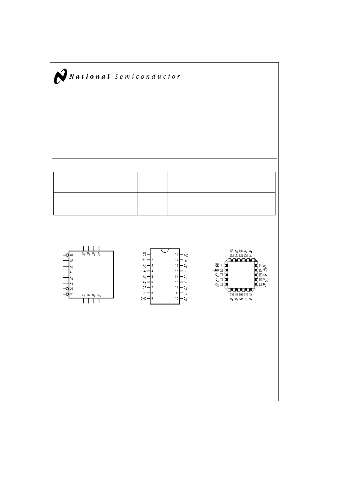
Logic Symbol
TL/F/9538– 3
Connection Diagrams
Pin Assignment
for DIP and SOIC
TL/F/9538– 1
Pin Assignment
for LCC
TL/F/9538– 2
TRI-STATEÉis a registered trademark of National Semiconductor Corporation.
C
1995 National Semiconductor Corporation RRD-B30M105/Printed in U. S. A.
Page 2
Unit Loading/Fan Out
54F/74F
Pin Names Description
U.L. Input I
IH/IIL
HIGH/LOW Output IOH/I
OL
A0–A
3
Address Inputs 1.0/1.0 20 mA/b0.6 mA
D
0–D3
Data Inputs 1.0/1.0 20 mA/b0.6 mA
CS
Chip Select Input (Active LOW) 1.0/2.0 20 mA/b1.2 mA
OE Output Enable Input (Active LOW) 1.0/1.0 20 mA/b0.6 mA
WE
Write Enable Input (Active LOW) 1.0/1.0 20 mA/b0.6 mA
CP Clock Input (Outputs Change on
LOW-to-HIGH Transition) 1.0/2.0 20 mA/
b
1.2 mA
Q
0–Q3
TRI-STATE Outputs 150/40 (33.3)b3 mA/24 mA (20 mA)
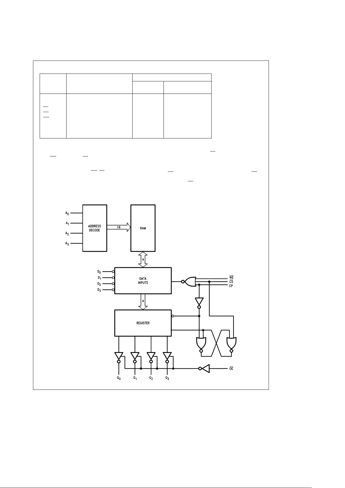
Functional Description
Write OperationÐWhen the three control inputs, Write En-
able (WE
), Chip Select (CS), and Clock (CP), are LOW the
information on the data inputs (D
0–D3
) is written into the
memory location selected by the address inputs (A
0–A3
). If
the input data changes while WE
,CS, and CP are LOW, the
contents of the selected memory location follow these
changes, provided setup and hold time criteria are met.
Read OperationÐWhenever CS
is LOW and CP goes from
LOW-to-HIGH, the contents of the memory location selected by the address inputs (A
0–A3
) are edge-triggered into
the Output Register.
The (OE
) input controls the output buffers. When OE is
HIGH the four outputs (Q
0–Q3
) are in a high impedance or
OFF state; when OE
is LOW, the outputs are determined by
the state of the Output Register.
Block Diagram
TL/F/9538– 4
2
Page 3
Absolute Maximum Ratings (Note 1)
If Military/Aerospace specified devices are required,
please contact the National Semiconductor Sales
Office/Distributors for availability and specifications.
Storage Temperature
b
65§Ctoa150§C
Ambient Temperature under Bias
b
55§Ctoa125§C
Junction Temperature under Bias
b
55§Ctoa175§C
Plastic
b
55§Ctoa150§C
V
CC
Pin Potential to
Ground Pin
b
0.5V toa7.0V
Input Voltage (Note 2)
b
0.5V toa7.0V
Input Current (Note 2)
b
30 mA toa5.0 mA
Voltage Applied to Output
in HIGH State (with V
CC
e
0V)
Standard Output
b
0.5V to V
CC
TRI-STATE Output
b
0.5V toa5.5V
Current Applied to Output
in LOW State (Max) twice the rated I
OL
(mA)
Note 1: Absolute maximum ratings are values beyond which the device may
be damaged or have its useful life impaired. Functional operation under
these conditions is not implied.
Note 2: Either voltage limit or current limit is sufficient to protect inputs.
Recommended Operating
Conditions
Free Air Ambient Temperature
Military
b
55§Ctoa125§C
Commercial 0
§
Ctoa70§C
Supply Voltage
Military
a
4.5V toa5.5V
Commercial
a
4.5V toa5.5V
DC Electrical Characteristics
Symbol Parameter
54F/74F
Units V
CC
Conditions
Min Typ Max
V
IH
Input HIGH Voltage 2.0 V Recognized as a HIGH Signal
V
IL
Input LOW Voltage 0.8 V Recognized as a LOW Signal
V
CD
Input Clamp Diode Voltage
b
1.2 V Min I
IN
eb
18 mA
V
OH
Output HIGH 54F 10% V
CC
2.5 I
OH
eb
1mA
Voltage 54F 10% V
CC
2.4 I
OH
eb
3mA
74F 10% V
CC
2.5 V Min I
OH
eb
1mA
74F 10% V
CC
2.4 I
OH
eb
3mA
74F 5% V
CC
2.7 I
OH
eb
3mA
V
OL
Output LOW 54F 10% V
CC
0.5
V Min
I
OL
e
20 mA
Voltage 74F 10% V
CC
0.5 I
OL
e
24 mA
I
IH
Input HIGH 54F 20.0
mA Max V
IN
e
2.7V
Current 74F 5.0
I
BVI
Input HIGH Current 54F 100
mA Max V
IN
e
7.0V
Breakdown Test 74F 7.0
I
CEX
Output HIGH 54F 250
mA Max V
OUT
e
V
CC
Leakage Current 74F 50
V
ID
Input Leakage
74F 4.75 V 0.0
I
ID
e
1.9 mA
Test All Other Pins Grounded
I
OD
Output Leakage
74F 3.75 mA 0.0
V
IOD
e
150 mV
Circuit Current All Other Pins Grounded
I
IL
Input LOW Current
b
0.6
mA Max
V
IN
e
0.5V (An,Dn,OE,WE)
b
1.2 V
IN
e
0.5V (CS, CP)
I
OZH
Output Leakage Current 50 mA Max V
OUT
e
2.7V
I
OZL
Output Leakage Current
b
50 mA Max V
OUT
e
0.5V
I
OS
Output Short-Circuit Current
b
60
b
150 mA Max V
OUT
e
0V
I
ZZ
Bus Drainage Test 500 mA 0.0V V
OUT
e
5.25V
3
Page 4

DC Electrical Characteristics (Continued)
Symbol Parameter
54F/74F
Units V
CC
Conditions
Min Typ Max
I
CCH
Power Supply Current 47 70 mA Max V
O
e
HIGH
I
CCL
Power Supply Current 47 70 mA Max V
O
e
LOW
I
CCZ
Power Supply Current 47 70 mA Max V
O
e
HIGH Z
AC Electrical Characteristics
74F 54F 74F
T
A
ea
25§C
T
A,VCC
e
Mil TA,V
CC
e
Com
Symbol Parameter V
CC
ea
5.0V
C
L
e
50 pF C
L
e
50 pF
Units
C
L
e
50 pF
Min Max Min Max Min Max
t
PLH
Propagation Delay 3.0 8.5 2.5 11.0 2.5 9.5
ns
t
PHL
CP to Q 3.5 9.0 3.0 12.0 3.0 10.0
t
PZH
Enable Time 3.0 8.0 2.5 10.5 2.5 9.0
t
PZL
OE to Q 3.5 9.0 3.0 13.0 3.0 10.0
t
PHZ
Disable Time 2.5 6.5 2.0 8.5 2.0 7.5
ns
t
PLZ
OE to Q 2.5 7.0 2.0 9.5 2.0 8.0
AC Operating Requirements
74F 54F 74F
Symbol Parameter
T
A
ea
25§C
T
A,VCC
e
Mil TA,V
CC
e
Com Units
V
CC
ea
5.0V
Min Max Min Max Min Max
READ MODE
ts(H) Setup Time, HIGH or LOW 15.0 23 17.0
t
s
(L) Anto CP 15.0 23 17.0
th(H) Hold Time, HIGH or LOW 0 0 0
ns
t
h
(L) Anto CP 0 0 0
WRITE MODE
ts(H) Setup Time, HIGH or LOW 0 0 0
t
s
(L) Anto WE 000
t
h
(H) Hold Time, HIGH or LOW 0 0 0
ns
t
h
(L) Anto WE 000
t
s
(H) Setup Time, HIGH or LOW 5.0 8.5 6.0
t
s
(L) Dnto WE 5.0 8.5 6.0
th(H) Hold Time, HIGH or LOW 0 2.5 0
ns
t
h
(L) Dnto WE 0 2.5 0
t
w
WE Pulse Width
7.5 9.5 8.5 ns
Required to Write
t
w
CS Pulse Width
7.5 9.5 8.5 ns
Required to Write
t
w
CP Pulse Width
7.5 9.5 8.5 ns
Required to Write
Note: Military temperature range for this device isb40§Ctoa85§C.
4
Page 5

Ordering Information
The device number is used to form part of a simplified purchasing code where a package type and temperature range are
defined as follows:
74F 410 S C X
Temperature Range Family Special Variations
74F
e
Commercial XeDevices shipped in 13×reels
54F
e
Military QBeMilitary grade device with
environmental and burn-in
Device Type
processing
Package Code
Temperature Range
P
e
Plastic DIP
C
e
Commercial (0§Ctoa70§C)
S
e
Small Outline (SOIC)
M
e
Military (b55§Ctoa125§C)
D
e
Ceramic DIP
L
e
Package Leadless Chip Carrier
5
Page 6

Physical Dimensions inches (millimeters)
18-Lead Ceramic Dual-In-Line Package (D)
NS Package Number J18A
20-Lead (0.300×Wide) Molded Small Outline Package, JEDEC (S)
NS Package Number M20B
6
Page 7

Physical Dimensions inches (millimeters) (Continued)
18-Lead (0.300×Wide) Molded Dual-In-Line Package (P)
NS Package Number N18A
7
Page 8

54F/74F410 Register StackÐ16 x 4 RAM TRI-STATE Output Register
Physical Dimensions inches (millimeters) (Continued)
20-Lead Cerpack
NS Package Number W20A
LIFE SUPPORT POLICY
NATIONAL’S PRODUCTS ARE NOT AUTHORIZED FOR USE AS CRITICAL COMPONENTS IN LIFE SUPPORT
DEVICES OR SYSTEMS WITHOUT THE EXPRESS WRITTEN APPROVAL OF THE PRESIDENT OF NATIONAL
SEMICONDUCTOR CORPORATION. As used herein:
1. Life support devices or systems are devices or 2. A critical component is any component of a life
systems which, (a) are intended for surgical implant support device or system whose failure to perform can
into the body, or (b) support or sustain life, and whose be reasonably expected to cause the failure of the life
failure to perform, when properly used in accordance support device or system, or to affect its safety or
with instructions for use provided in the labeling, can effectiveness.
be reasonably expected to result in a significant injury
to the user.
National Semiconductor National Semiconductor National Semiconductor National Semiconductor
Corporation Europe Hong Kong Ltd. Japan Ltd.
1111 West Bardin Road Fax: (
a
49) 0-180-530 85 86 13th Floor, Straight Block, Tel: 81-043-299-2309
Arlington, TX 76017 Email: cnjwge@tevm2.nsc.com Ocean Centre, 5 Canton Rd. Fax: 81-043-299-2408
Tel: 1(800) 272-9959 Deutsch Tel: (
a
49) 0-180-530 85 85 Tsimshatsui, Kowloon
Fax: 1(800) 737-7018 English Tel: (
a
49) 0-180-532 78 32 Hong Kong
Fran3ais Tel: (
a
49) 0-180-532 93 58 Tel: (852) 2737-1600
Italiano Tel: (
a
49) 0-180-534 16 80 Fax: (852) 2736-9960
National does not assume any responsibility for use of any circuitry described, no circuit patent licenses are implied and National reserves the right at any time without notice to change said circuitry and specifications.
 Loading...