

Page 1
查询54F322供应商
54F/74F322
Octal Serial/Parallel Register with Sign Extend
54F/74F322 Octal Serial/Parallel Register with Sign Extend
May 1995
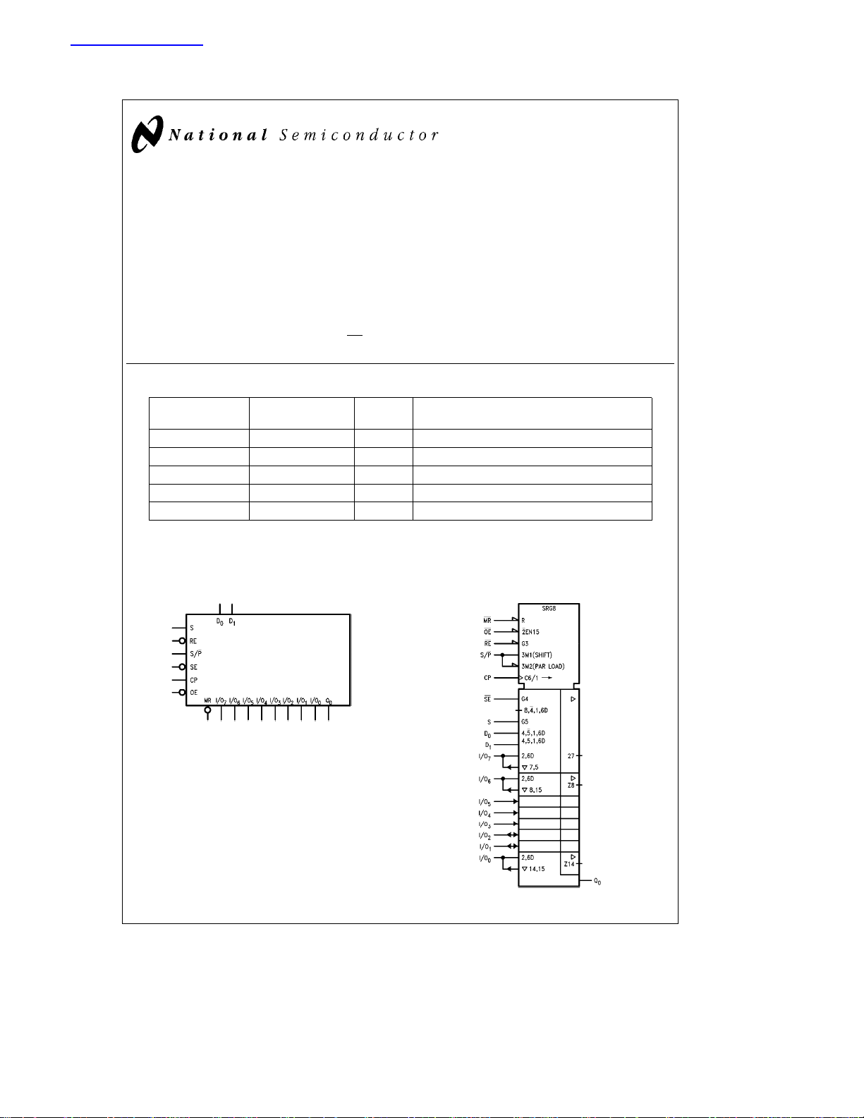
General Description
The ’F322 is an 8-bit shift register with provision for either
serial or parallel loading and with TRI-STATE
puts plus a bi-state serial output. Parallel data inputs and
parallel outputs are multiplexed to minimize pin count. State
changes are initiated by the rising edge of the clock. Four
synchronous modes of operation are possible: hold (store),
shift right with serial entry, shift right with sign extend and
parallel load. An asynchronous Master Reset (MR
overrides clocked operation and clears the register.
Commercial Military
74F322PC N20A 20-Lead (0.300×Wide) Molded Dual-In-Line
54F322DM (Note 2) J20A 20-Lead Ceramic Dual-In-Line
74F322SJ (Note 1) M20D 20-Lead (0.300×Wide) Molded Small Outline, EIAJ
54F322FM (Note 2) W20A 20-Lead Cerpack
54F322LM (Note 2) E20A 20-Lead Ceramic Leadless Chip Carrier, Type C
Note 1: Devices also available in 13×reel. Use suffixeSJX.
Note 2: Military grade device with environmental and burn-in processing. Use suffix
parallel out-
É
) input
Package
Number
Features
Y
Multiplexed parallel I/O ports
Y
Separate serial input and output
Y
Sign extend function
Y
TRI-STATE outputs for bus applications
Package Description
e
DMQB, FMQB and LMQB.
Logic Symbols
IEEE/IEC
TL/F/9516– 3
TL/F/9516– 5
TRI-STATEÉis a registered trademark of National Semiconductor Corporation.
C
1995 National Semiconductor Corporation RRD-B30M105/Printed in U. S. A.
TL/F/9516
Page 2
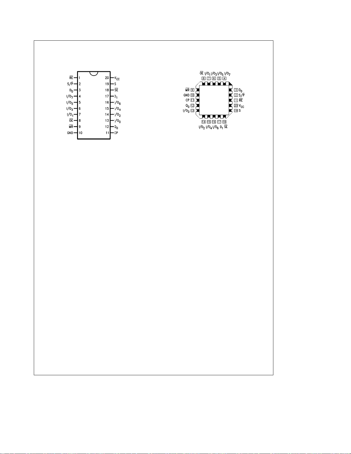
Connection Diagrams
Pin Assignment
for DIP, SOIC and Flatpak
Pin Assignment
for LCC
TL/F/9516– 2
TL/F/9516– 1
2
Page 3
Unit Loading/Fan Out
54F/74F
Pin Names Description
U.L. Input I
HIGH/LOW Output IOH/I
IH/IIL
OL
RE Register Enable Input (Active LOW) 1.0/1.0 20 mA/b0.6 mA
S/P
SE
Serial (HIGH) or Parallel (LOW) Mode Control Input 1.0/1.0 20 mA/b0.6 mA
Sign Extend Input (Active LOW) 1.0/3.0 20 mA/b1.8 mA
S Serial Data Select Input 1.0/2.0 20 mA/b1.2 mA
D
0,D1
CP Clock Pulse Input (Active Rising Edge) 1.0/1.0 20 mA/b0.6 mA
MR
OE
Q
0
I/O
Serial Data Inputs 1.0/1.0 20 mA/b0.6 mA
Asynchronous Master Reset Input (Active LOW) 1.0/1.0 20 mA/b0.6 mA
TRI-STATE Output Enable Input (Active LOW) 1.0/1.0 20 mA/b0.6 mA
Bi-State Serial Output 50/33.3
–I/O7Multiplexed Parallel Data Inputs or 3.5/1.083 70 mA/b0.65 mA
0
TRI-STATE Parallel Data Outputs 150/40 (33.3)
b
1 mA/b20 mA
b
3 mA/24 mA (20 mA)
Functional Description
The ’F322 contains eight D-type edge triggered flip-flops
and the interstage gating required to perform right shift and
the intrastage gating necessary for hold and synchronous
parallel load operations. A LOW signal on RE
enables shifting or parallel loading, while a HIGH signal enables the hold
mode. A HIGH signal on S/P
enables shift right, while a
LOW signal disables the TRI-STATE output buffers and enables parallel loading. In the shift right mode a HIGH signal
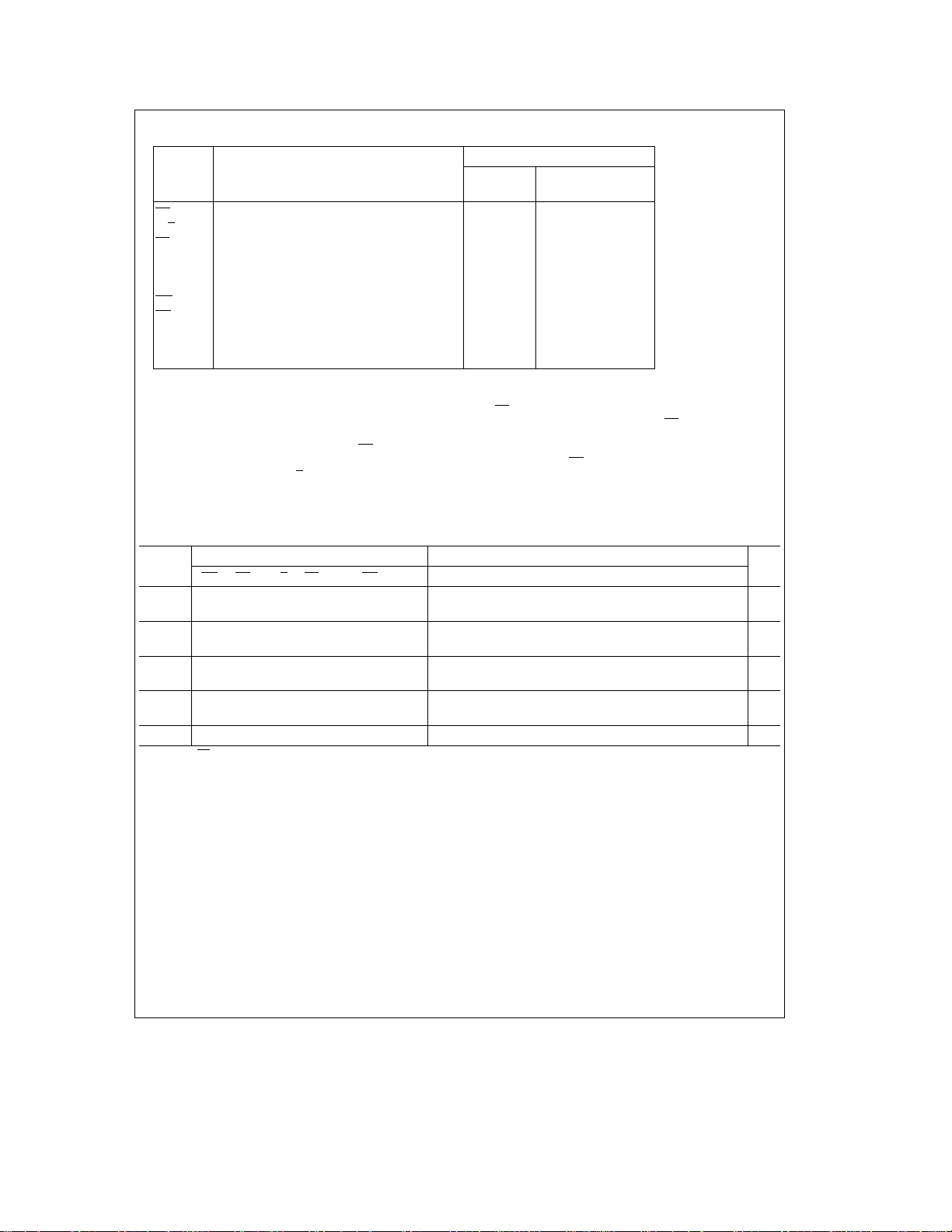
Mode Select Table
Mode
Inputs Outputs
MR RE S/P SE SOE* CP I/O7I/O6I/O5I/O4I/O3I/O2I/O1I/O
Clear L X X X X L X L L L L L L L L L
LXXXXHXZZZZZZZZL
Parallel
Load
HL L XXXLI
Shift H L H H L L L D
Right H L H H H L L D
Sign
Extend
HLHLXLLO
Hold H H X X X L L NC NC NC NC NC NC NC NC NC
*When the OE input is HIGH all I/Onterminals are at the high impedance state; sequential operation or clearing of the register is not affected.
Note 1: I
the I/O terminal.
Note 2: D
Note 3: O
H
L
Z
L
NC
e
The level of the steady-state input at the respective I/O terminal is loaded into the flip-flop while the flip-flop outputs (except Q0) are isolated from
7–I0
e
The level of the steady-state inputs to the serial multiplexer input.
0,D1
e
The level of the respective Qnflip-flop prior to the last Clock LOW-to-HIGH transition.
7–O0
e
HIGH Voltage Level
e
LOW Voltage Level
e
High Impedance Output State
e
LOW-to-HIGH Transition
e
No Change
on SE
enables serial entry from either D0or D1, as determined by the S input. A LOW signal on SE
but Q
reloads its contents, thus performing the sign extend
7
function required for the ’F384 Twos Complement Multiplier.
A HIGH signal on OE
disables the TRI-STATE output buff-
enables shift right
ers, regardless of the other control inputs. In this condition
the shifting and loading operations can still be performed.
Q
0
7I6I5I4I3I2I1I0I0
O
O
O
0
7
O
1
O7O6O5O4O3O2O1O
7
6
O
7
6
O4O
5
O
O4O
5
O
3
3
O1O
2
O
O1O
2
0
1
1
1
3
Page 4

Logic Diagram
Please note that this diagram is provided only for the understanding of logic operations and should not be used to estimate propagation delays.
4
TL/F/9516– 4
Page 5

Absolute Maximum Ratings (Note 1)
If Military/Aerospace specified devices are required,
please contact the National Semiconductor Sales
Office/Distributors for availability and specifications.
Storage Temperature
Ambient Temperature under Bias
Junction Temperature under Bias
Plastic
Pin Potential to
V
CC
Ground Pin
Input Voltage (Note 2)
Input Current (Note 2)
Note 1: Absolute maximum ratings are values beyond which the device may
be damaged or have its useful life impaired. Functional operation under
these conditions is not implied.
Note 2: Either voltage limit or current limit is sufficient to protect inputs.
b
65§Ctoa150§C
b
55§Ctoa125§C
b
55§Ctoa175§C
b
55§Ctoa150§C
b
0.5V toa7.0V
b
0.5V toa7.0V
b
30 mA toa5.0 mA
DC Electrical Characteristics
Symbol Parameter
V
V
V
V
V
I
IH
I
BVI
I
BVIT
I
CEX
V
I
OD
I
IL
I
IH
I
OZH
I
IL
I
OZL
I
OS
I
ZZ
I
CC
Input HIGH Voltage 2.0 V Recognized as a HIGH Signal
IH
Input LOW Voltage 0.8 V Recognized as a LOW Signal
IL
Input Clamp Diode Voltage
CD
Output HIGH 54F 10% VCC2.5 I
OH
Voltage 54F 10% V
Output LOW 54F 10% V
OL
Voltage 74F 10% V
Input HIGH 54F 20.0
Current 74F 5.0
Input HIGH Current 54F 100
Breakdown Test 74F 7.0
Input HIGH Current 54F 1.0
Breakdown Test (I/O) 74F 0.5
Output HIGH 54F 250
Leakage Current 74F 50
Input Leakage
ID
Test All Other Pins Grounded
Output Leakage
Circuit Current All Other Pins Grounded
Input LOW Current
a
Output Leakage Current
a
Output Leakage Current
Output Short-Circuit Current
Bus Drainage Test 500 mA 0.0V V
Power Supply Current 60 90 mA Max
74F 10% V
74F 10% V
74F 5% V
74F 5% V
74F 10% V
74F 4.75 V 0.0
74F 3.75 mA 0.0
Min Typ Max
2.4 I
CC
2.5
CC
2.4 I
CC
2.7 I
CC
2.7 I
CC
CC
CC
CC
b
60
54F/74F
Voltage Applied to Output
in HIGH State (with V
Standard Output
CC
e
0V)
TRI-STATE Output
Current Applied to Output
in LOW State (Max) twice the rated I
Recommended Operating
Conditions
Free Air Ambient Temperature
Military
Commercial 0
Supply Voltage
Military
Commercial
Units V
b
1.2 V Min I
CC
V Min
0.5 I
0.5 V Min I
0.5 I
mA Max
mA Max
mA Max
mA Max
b
0.6 mA Max V
b
1.2 mA Max V
b
1.8 mA Max V
70 mA Max V
b
650 mA Max
b
150 mA Max V
I
V
V
V
V
I
V
V
IN
OH
OH
OH
OH
OH
OH
OL
OL
OL
IN
IN
IN
OUT
ID
IOD
IN
IN
IN
I/O
I/O
OUT
OUT
eb
e
e
e
Conditions
18 mA
eb
1mA(Q0, I/On)
eb
3 mA (I/On)
eb
1mA(Q0, I/On)
eb
3 mA (I/On)
eb
1mA(Q0, I/On)
eb
3 mA (I/On)
e
20 mA (Q0, I/On)
e
20 mA (Q0)
e
24 mA ( I/On)
e
2.7V
e
7.0V (Non-I/O Inputs)
e
5.5V (I/On)
e
V
CC
1.9 mA
e
150 mV
e
0.5V (RE, S/P,Dn, CP, MR,OE)
0.5V (S)
0.5V (SE)
e
2.7V (I/On)
e
0.5V (I/On)
e
0V
e
5.25V
b
0.5V to V
b
0.5V toa5.5V
OL
b
55§Ctoa125§C
Ctoa70§C
§
a
4.5V toa5.5V
a
4.5V toa5.5V
CC
(mA)
5
Page 6

AC Electrical Characteristics
74F 54F 74F
Symbol Parameter V
A
ea
5.0V
CC
e
50 pF
C
L
T
A,VCC
e
50 pF C
C
L
e
Mil TA,V
ea
T
25§C
Min Typ Max Min Max Min Max
f
t
t
t
t
t
t
t
t
t
t
t
t
t
t
max
PLH
PHL
PLH
PHL
PHL
PHL
PZH
PZL
PHZ
PLZ
PZH
PZL
PHZ
PLZ
Maximum Clock Frequency 70 90 50 70 MHz
Propagation Delay 3.5 7.0 7.5 3.5 9.5 3.5 8.5
CP to I/O
n
5.0 8.5 11.0 3.5 10.0 5.0 12.0
Propagation Delay 3.5 7.0 9.0 3.5 11.0 3.5 10.0
CP to Q
0
Propagation Delay
to I/O
MR
n
Propagation Delay
MR to Q
0
3.5 7.0 8.0 3.5 10.0 3.5 9.0
6.0 10.0 13.0 6.0 15.0 6.0 14.0 ns
5.5 7.5 12.0 5.5 14.0 5.5 13.0 ns
Output Enable Time 3.0 6.5 9.0 3.0 12.5 3.0 10.0
OE to I/O
n
4.0 8.5 11.0 4.0 14.5 4.0 12.0
Output Disable Time 2.0 4.5 6.0 2.0 8.0 2.0 7.0
OE to I/O
n
2.0 5.0 7.0 2.0 10.0 2.0 8.0
Output Enable Time 4.5 8.0 10.5 4.5 13.5 4.5 11.5
S/P to I/O
n
5.5 10.0 14.0 5.5 17.0 5.5 15.0
Output Disable Time 5.0 9.0 11.5 5.0 16.5 5.0 12.5
S/P to I/O
n
6.0 12.0 15.5 6.0 19.5 6.0 16.5
AC Operating Requirements
74F 54F 74F
ea
T
25§C
Symbol Parameter
A
ea
CC
5.0V
V
Min Max Min Max Min Max
ts(H) Setup Time, HIGH or LOW 6.0 14.0 7.0
(L) RE to CP 14.0 18.0 16.0
t
s
th(H) Hold Time, HIGH or LOW 0 0 0
(L) RE to CP 0 0 0
t
h
ts(H) Setup Time, HIGH or LOW 6.5 8.5 7.5
(L) D0,D1or I/Onto CP 6.5 8.5 7.5
t
s
th(H) Hold Time, HIGH or LOW 2.0 3.0 3.0
(L) D0,D1or I/Onto CP 2.0 3.0 3.0
t
h
ts(H) Setup Time, HIGH or LOW 7.0 9.0 8.0
ts(L) SE to CP 2.5 11.0 3.5
th(H) Hold Time, HIGH or LOW 2.0 2.0 2.0
(L) SE to CP 0.0 1.0 0.0
t
h
ts(H) Setup Time, HIGH or LOW 11.0 13.0 12.0
(L) S/P to CP 13.5 21.0 15.5
t
s
ts(H) Setup Time, HIGH or LOW 6.5 8.5 7.5
ts(L) S to CP 9.0 11.0 10.0
th(H) Hold Time, HIGH or LOW 0 1.0 0
(L) S or S/P to CP 0 0 0
t
h
tw(H) CP Pulse Width, HIGH or LOW
(L)
t
w
7.0 8.0 7.0 ns
tw(L) MR Pulse Width, LOW 5.5 7.5 6.5
t
rec
Recovery Time
MR to CP
8.0 12.0 8.0 ns
6
T
A,VCC
e
Mil TA,V
e
CC
e
50 pF
L
e
CC
Com
Units
ns
ns
ns
Com Units
ns
ns
ns
ns
ns
ns
ns
ns
ns
Page 7

Ordering Information
The device number is used to form part of a simplified purchasing code where the package type and temperature range are
defined as follows:
74F 322 S C X
Temperature Range Family Special Variations
e
74F
Commercial QBeMilitary grade device with
e
54F
Military environmental and burn-in
Device Type
Package Code
e
Plastic DIP
P
e
Ceramic DIP
D
e
Flatpak
F
e
SJ
Small Outline SOIC EIAJ
e
L
Leadless Chip Carrier (LCC)
processing
e
Devices shipped in 13×reel
X
Temperature Range
e
Commercial (0§Ctoa70§C)
C
e
Military (b55§Ctoa125§C)
M
Physical Dimensions inches (millimeters)
20-Lead Ceramic Leadless Chip Carrier (L)
NS Package Number E20A
7
Page 8

Physical Dimensions inches (millimeters) (Continued)
20-Lead Ceramic Dual-In-Line Package (D)
NS Package Number J20A
8
Page 9

Physical Dimensions inches (millimeters) (Continued)
20-Lead (0.300×Wide) Molded Small Outline Package, EIAJ (SJ)
20-Lead (0.300×Wide) Molded Dual-In-Line Package (P)
NS Package Number M20D
NS Package Number N20A
9
Page 10

Physical Dimensions inches (millimeters) (Continued)
20-Lead Ceramic Flatpak (F)
NS Package Number W20A
54F/74F322 Octal Serial/Parallel Register with Sign Extend
LIFE SUPPORT POLICY
NATIONAL’S PRODUCTS ARE NOT AUTHORIZED FOR USE AS CRITICAL COMPONENTS IN LIFE SUPPORT
DEVICES OR SYSTEMS WITHOUT THE EXPRESS WRITTEN APPROVAL OF THE PRESIDENT OF NATIONAL
SEMICONDUCTOR CORPORATION. As used herein:
1. Life support devices or systems are devices or 2. A critical component is any component of a life
systems which, (a) are intended for surgical implant support device or system whose failure to perform can
into the body, or (b) support or sustain life, and whose be reasonably expected to cause the failure of the life
failure to perform, when properly used in accordance support device or system, or to affect its safety or
with instructions for use provided in the labeling, can effectiveness.
be reasonably expected to result in a significant injury
to the user.
National Semiconductor National Semiconductor National Semiconductor National Semiconductor
Corporation Europe Hong Kong Ltd. Japan Ltd.
1111 West Bardin Road Fax: (
Arlington, TX 76017 Email: cnjwge@tevm2.nsc.com Ocean Centre, 5 Canton Rd. Fax: 81-043-299-2408
Tel: 1(800) 272-9959 Deutsch Tel: (
Fax: 1(800) 737-7018 English Tel: (
National does not assume any responsibility for use of any circuitry described, no circuit patent licenses are implied and National reserves the right at any time without notice to change said circuitry and specifications.
Fran3ais Tel: (
Italiano Tel: (
a
49) 0-180-530 85 86 13th Floor, Straight Block, Tel: 81-043-299-2309
a
49) 0-180-530 85 85 Tsimshatsui, Kowloon
a
49) 0-180-532 78 32 Hong Kong
a
49) 0-180-532 93 58 Tel: (852) 2737-1600
a
49) 0-180-534 16 80 Fax: (852) 2736-9960
 Loading...