

Page 1
TL/F/9492
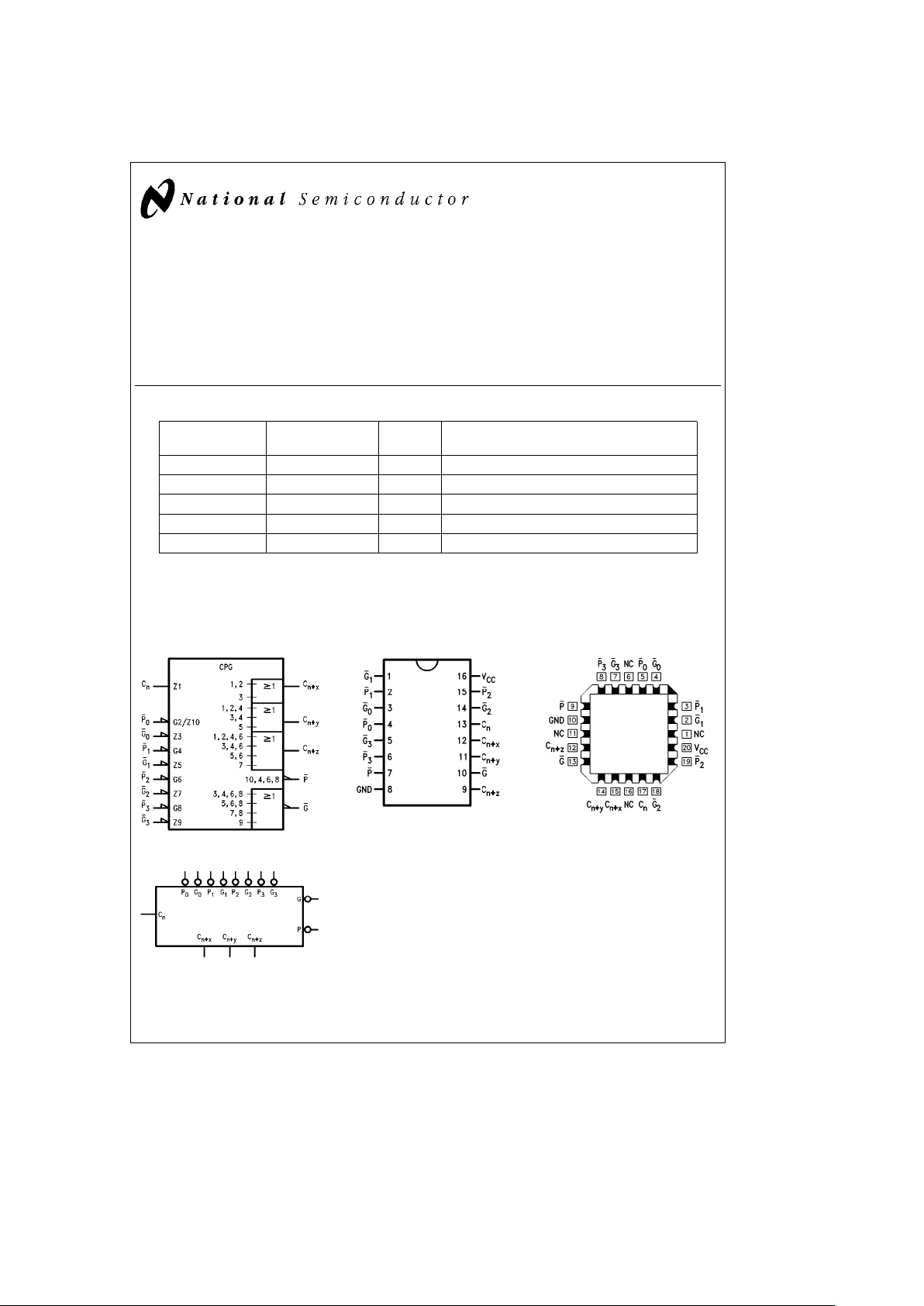
54F/74F182 Carry Lookahead Generator
December 1994
54F/74F182
Carry Lookahead Generator
General Description
The ’F182 is a high-speed carry lookahead generator. It is
generally used with the ’F181 or ’F381 4-bit arithmetic logic
units to provide high-speed lookahead over word lengths of
more than four bits.
Features
Y
Provides lookahead carries across a group of four
ALUs
Y
Multi-level lookahead high-speed arithmetic operation
over long word lengths
Y
Guaranteed 4000V minimum ESD protection
Commercial Military
Package
Package Description
Number
74F182PC N16E 16-Lead (0.300×Wide) Molded Dual-In-Line
54F182DM (Note 2) J16A 16-Lead Ceramic Dual-In-Line
74F182SJ (Note 1) M16D 16-Lead (0.300×Wide) Molded Small Outline, EIAJ
54F182FM (Note 2) W16A 16-Lead Cerpack
54F182LM (Note 2) E20A 20-Lead Ceramic Leadless Chip Carrier, Type C
Note 1: Devices also available in 13×reel. Use suffixeSCX and SJX.
Note 2: Military grade device with environmental and burn-in processing. Use suffix
e
DMQB, FMQB and LMQB
Logic Symbols Connection Diagrams
IEEE/IEC
TL/F/9492– 6
TL/F/9492– 3
Pin Assignment for
DIP, SOIC and Flatpak
TL/F/9492– 1
Pin Assignment
for LCC
TL/F/9492– 2
TRI-STATEÉis a registered trademark of National Semiconductor Corporation.
C
1995 National Semiconductor Corporation RRD-B30M105/Printed in U. S. A.
Page 2
Unit Loading/Fan Out
54F/74F
Pin Names Description
U.L. Input I
IH/IIL
HIGH/LOW Output IOH/I
OL
C
n
Carry Input 1.0/2.0 20 mA/b1.2 mA
G
0,G2
Carry Generate Inputs (Active LOW) 1.0/14.0 20 mA/b8.4 mA
G
1
Carry Generate Input (Active LOW) 1.0/16.0 20 mA/b9.6 mA
G
3
Carry Generate Input (Active LOW) 1.0/8.0 20 mA/b4.8 mA
P
0,P1
Carry Propagate Inputs (Active LOW) 1.0/8.0 20 m A/b4.8 mA
P
2
Carry Propagate Input (Active LOW) 1.0/6.0 20 mA/b3.6 mA
P
3
Carry Propagate Input (Active LOW) 1.0/4.0 20 mA/b2.4 mA
C
nax
b
C
naz
Carry Outputs 50/33.3
b
1 mA/20 mA
G
Carry Generate Output (Active LOW) 50/33.3
b
1 mA/20 mA
P
Carry Propagate Output (Active LOW) 50/33.3
b
1 mA/20 mA
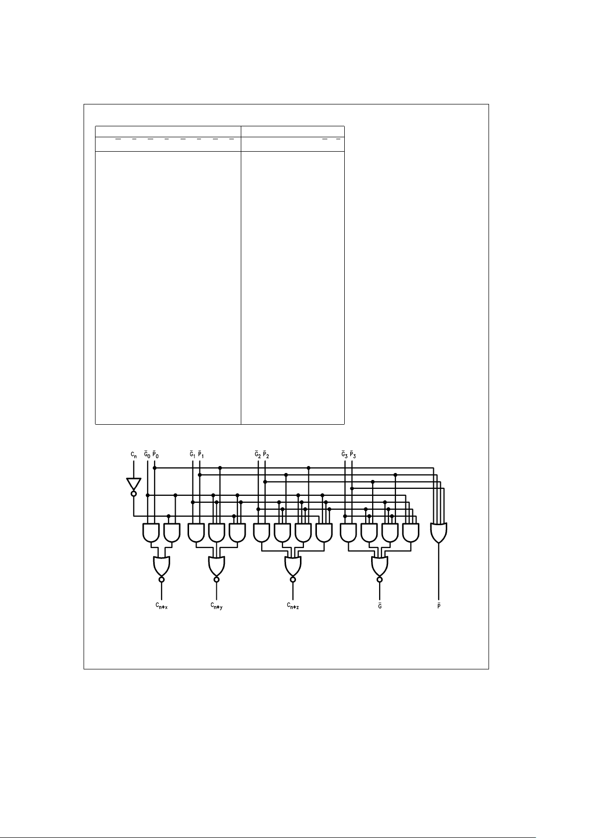
Functional Description
The ’F182 carry lookahead generator accepts up to four
pairs of Active LOW Carry Propagate (P
0–P3
) and Carry
Generate (G
0–G3
) signals and an Active HIGH Carry input
(C
n
) and provides anticipated Active HIGH carries (C
nax
,
C
nay,Cnaz
) across four groups of binary adders. The
’F182 also has Active LOW Carry Propagate (P
) and Carry
Generate (G
) outputs which may be used for further levels
of lookahead. The logic equations provided at the outputs
are:
C
nax
e
G
0
a
P0C
n
C
nay
e
G
1
a
P1G
0
a
P1P0C
n
C
naz
e
G
2
a
P2G
1
a
P2P1G
0
a
P2P1P0C
n
G
e
G
3
a
P3G
2
a
P3P2G
1
a
P3P2P1G
0
P
e
P2P2P1P
0
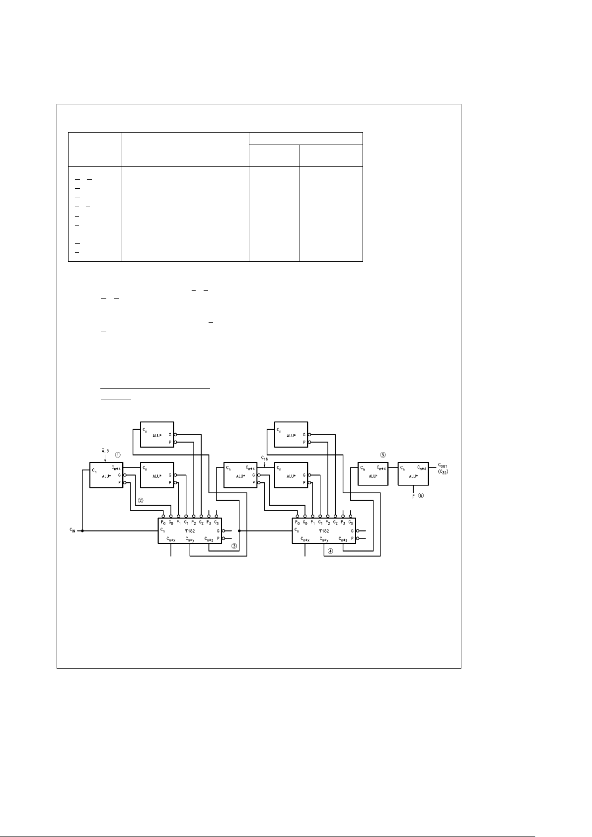
Also, the ’F182 can be used with binary ALUs in an active
LOW or active HIGH input operand mode. The connections
(Figure 1)
to and from the ALU to the carry lookahead generator are identical in both cases. Carries are rippled between lookahead blocks. The critical speed path follows the
circled numbers. There are several possible arrangements
for the carry interconnects, but all achieve about the same
speed. A 28-bit ALU is formed by dropping the last ’F181 or
’F381.
TL/F/9492– 5
FIGURE 1. 32-Bit ALU with Rippled Carry between 16-Bit Lookahead ALUs
*ALUs may be either ’F181 or ’F381
2
Page 3
Truth Table
Inputs Outputs
CnG0P0G1P1G2P2G3P3C
naxCnayCnaz
G P
XHH L
LHX L
XLX H
HXL H
XXXHH L
XHHH X L
LHXHX L
XXXLX H
XLXXL H
HXLXL H
XXXXXHH L
X XXHHHX L
XHHHXHX L
LHXHXHX L
XXXXXL X H
XXXLXXL H
XLXXLXL H
HXLXLXL H
X XXXXHH H
XXXHHHX H
X HHHXHX H
H HXHXHX H
X XXXXLX L
X XXLXXL L
XLXXLXL L
L XLXLXL L
HXXX H
XHXX H
XXHX H
XXXH H
LLLL L
H
e
HIGH Voltage Level
L
e
LOW Voltage Level
X
e
Immaterial
Logic Diagram
TL/F/9492– 4
Please note that this diagram is provided only for the understanding of logic operations and should not be used to estimate propagation delays.
3
Page 4

Absolute Maximum Ratings (Note 1)
If Military/Aerospace specified devices are required,
please contact the National Semiconductor Sales
Office/Distributors for availability and specifications.
Storage Temperature
b
65§Ctoa150§C
Ambient Temperature under Bias
b
55§Ctoa125§C
Junction Temperature under Bias
b
55§Ctoa175§C
Plastic
b
55§Ctoa150§C
V
CC
Pin Potential to
Ground Pin
b
0.5V toa7.0V
Input Voltage (Note 2)
b
0.5V toa7.0V
Input Current (Note 2)
b
30 mA toa5.0 mA
Voltage Applied to Output
in HIGH State (with V
CC
e
0V)
Standard Output
b
0.5V to V
CC
TRI-STATEÉOutput
b
0.5V toa5.5V
Current Applied to Output
in LOW State (Max) twice the rated I
OL
(mA)
ESD Last Passing Voltage (Min) 4000V
Note 1: Absolute maximum ratings are values beyond which the device may
be damaged or have its useful life impaired. Functional operation under
these conditions is not implied.
Note 2: Either voltage limit or current limit is sufficient to protect inputs.
Recommended Operating
Conditions
Free Air Ambient Temperature
Military
b
55§Ctoa125§C
Commercial 0
§
Ctoa70§C
Supply Voltage
Military
a
4.5V toa5.5V
Commercial
a
4.5V toa5.5V
DC Electrical Characteristics
Symbol Parameter
54F/74F
Units V
CC
Conditions
Min Typ Max
V
IH
Input HIGH Voltage 2.0 V Recognized as a HIGH Signal
V
IL
Input LOW Voltage 0.8 V Recognized as a LOW Signal
V
CD
Input Clamp Diode Voltage
b
1.2 V Min I
IN
eb
18 mA
V
OH
Output HIGH 54F 10% V
CC
2.5 I
OH
eb
1mA
Voltage 74F 10% V
CC
2.5 V Min I
OH
eb
1mA
74F 5% V
CC
2.7 I
OH
eb
1mA
V
OL
Output LOW 54F 10% V
CC
0.5
V Min
I
OL
e
20 mA
Voltage 74F 10% V
CC
0.5 I
OL
e
20 mA
I
IH
Input HIGH 54F 20.0
mA Max
V
IN
e
2.7V
Current 74F 5.0
I
BVI
Input HIGH Current 54F 100
mA Max
V
IN
e
7.0V
Breakdown Test 74F 7.0
I
CEX
Output HIGH 54F 250
mA Max
V
OUT
e
V
CC
Leakage Current 74F 50
V
ID
Input Leakage
74F 4.75 V 0.0
I
ID
e
1.9 mA
Test All Other Pins Grounded
I
OD
Output Leakage
74F 3.75 mA 0.0
V
IOD
e
150 mV
Circuit Current All Other Pins Grounded
I
IL
Input LOW
b
1.2 V
IN
e
0.5V (Cn)
Current
b
2.4 V
IN
e
0.5V (P3)
b
3.6
mA Max
V
IN
e
0.5V (P2)
b
4.8 V
IN
e
0.5V (G3,P0,P1)
b
8.4 V
IN
e
0.5V (G0,G2)
b
9.6 V
IN
e
0.5V (G1)
I
OS
Output Short-Circuit Current
b
60
b
150 mA Max V
OUT
e
0V
I
CCH
Power Supply Current 18.4 28.0 mA Max V
O
e
HIGH
I
CCL
Power Supply Current 23.5 36.0 mA Max V
O
e
LOW
4
Page 5

AC Electrical Characteristics
74F 54F 74F
T
A
ea
25§C
T
A,VCC
e
Mil TA,V
CC
e
Com
Symbol Parameter V
CC
ea
5.0V
C
L
e
50 pF C
L
e
50 pF
Units
C
L
e
50 pF
Min Typ Max Min Max Min Max
t
PLH
Propagation Delay 3.0 6.6 8.5 3.0 12.0 3.0 9.5
ns
t
PHL
Cnto C
nax,Cnay,Cnaz
3.0 6.8 9.0 3.0 11.0 3.0 10.0
t
PLH
Propagation Delay
2.5 6.2 8.0 2.5 11.0 2.5 9.0
t
PHL
P0,P1,orP2to
1.5 3.7 5.0 1.0 7.0 1.5 6.0
ns
C
nax,Cnay
,orC
naz
t
PLH
Propagation Delay
2.5 6.5 8.5 2.5 11.0 2.5 9.5
t
PHL
G0,G1,orG2to
1.5 3.9 5.2 1.0 7.0 1.5 6.0
ns
C
nax,Cnay
,orC
naz
t
PLH
Propagation Delay 3.0 7.9 10.0 3.0 12.0 3.0 11.0
ns
t
PHL
P1,P2,orP3to G 3.0 6.0 8.0 2.5 10.0 3.0 9.0
t
PLH
Propagation Delay 3.0 8.3 10.5 3.0 12.0 3.0 11.5
ns
t
PHL
Gnto G 3.0 5.7 7.5 2.5 10.0 3.0 8.5
t
PLH
Propagation Delay 3.0 5.7 7.5 2.5 10.0 3.0 8.5
ns
t
PHL
Pnto P 2.5 4.1 5.5 2.5 8.0 2.5 6.5
Ordering Information
The device number is used to form part of a simplified purchasing code where the package type and temperature range are
defined as follows:
74F 182 P C QB
Temperature Range Family Special Variations
74F
e
Commercial QBeMilitary grade with
54F
e
Military environmental and burn-in
processing shipped in tubes
Device Type
Temperature Range
Package Code
C
e
Commercial (0§Ctoa70§C)
P
e
Plastic DIP
M
e
Military (b55§Ctoa125§C)
D
e
Ceramic DIP
F
e
Flatpak
L
e
Leadless Chip Carrier (LCC)
SJ
e
Small Outline SOIC EIAJ
5
Page 6

Physical Dimensions inches (millimeters)
20-Lead Ceramic Leadless Chip Carrier (L)
NS Package Number E20A
16-Lead Ceramic Dual-In-Line Package (D)
NS Package Number J16A
6
Page 7

Physical Dimensions inches (millimeters) (Continued)
16-Lead (0.300×Wide) Molded Small Outline Package, EIAJ (SJ)
NS Package Number M16D
16-Lead (0.300×Wide) Molded Dual-In-Line Package (P)
NS Package Number N16E
7
Page 8

54F/74F182 Carry Lookahead Generator
Physical Dimensions inches (millimeters) (Continued)
16-Lead Ceramic Flatpak (F)
NS Package Number W16A
LIFE SUPPORT POLICY
NATIONAL’S PRODUCTS ARE NOT AUTHORIZED FOR USE AS CRITICAL COMPONENTS IN LIFE SUPPORT
DEVICES OR SYSTEMS WITHOUT THE EXPRESS WRITTEN APPROVAL OF THE PRESIDENT OF NATIONAL
SEMICONDUCTOR CORPORATION. As used herein:
1. Life support devices or systems are devices or 2. A critical component is any component of a life
systems which, (a) are intended for surgical implant support device or system whose failure to perform can
into the body, or (b) support or sustain life, and whose be reasonably expected to cause the failure of the life
failure to perform, when properly used in accordance support device or system, or to affect its safety or
with instructions for use provided in the labeling, can effectiveness.
be reasonably expected to result in a significant injury
to the user.
National Semiconductor National Semiconductor National Semiconductor National Semiconductor
Corporation Europe Hong Kong Ltd. Japan Ltd.
1111 West Bardin Road Fax: (
a
49) 0-180-530 85 86 13th Floor, Straight Block, Tel: 81-043-299-2309
Arlington, TX 76017 Email: cnjwge@tevm2.nsc.com Ocean Centre, 5 Canton Rd. Fax: 81-043-299-2408
Tel: 1(800) 272-9959 Deutsch Tel: (
a
49) 0-180-530 85 85 Tsimshatsui, Kowloon
Fax: 1(800) 737-7018 English Tel: (
a
49) 0-180-532 78 32 Hong Kong
Fran3ais Tel: (
a
49) 0-180-532 93 58 Tel: (852) 2737-1600
Italiano Tel: (
a
49) 0-180-534 16 80 Fax: (852) 2736-9960
National does not assume any responsibility for use of any circuitry described, no circuit patent licenses are implied and National reserves the right at any time without notice to change said circuitry and specifications.
 Loading...