

Page 1
查询54ACT74供应商
December 1994
54F/74F11
Triple 3-Input AND Gate
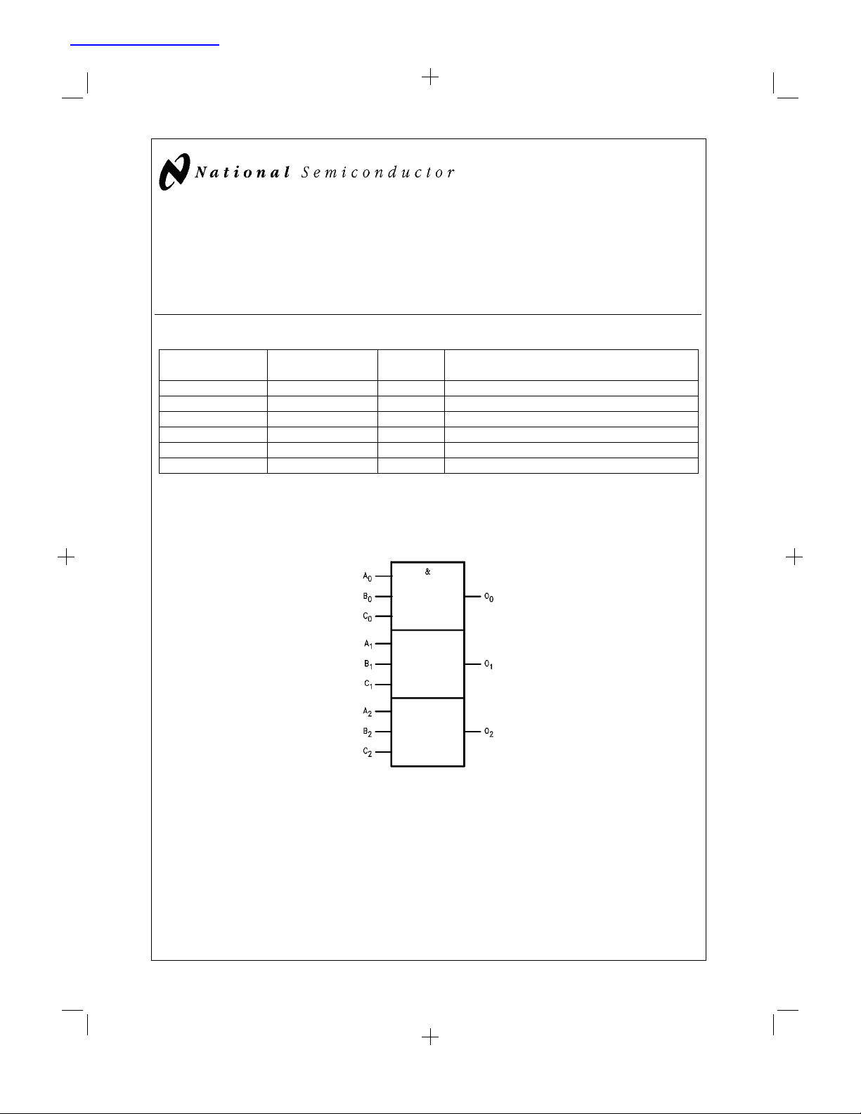
General Description
This device contains three independent gates, each of which
performs the logic AND function.
Ordering Code: See Section 0
Commercial Military Package Package Description
Number
74F11PC N14A 14-Lead (0.300" Wide) Molded Dual-In-Line
54F11DM (Note 2) J14A 14-Lead Ceramic Dual-In-Line
74F11SC (Note 1) M14A 14-Lead (0.150" Wide) Molded Small Outline, JEDEC
74F11SJ (Note 1) M14D 14-Lead (0.300" Wide) Molded Small Outline, EIAJ
54F11FM (Note 2) W14B 14-Lead Cerpack
54F11LM (Note 2) E20A 20-Lead Ceramic Leadless Chip Carrier, Type C
Note 1: Devices also available in 13" reel. Use suffix=SCX and SJX.
Note 2: Military grade device with environmental and burn-in processing. Use suffix=DMQB, FMQB and LMQB.
Logic Symbol
54F/74F11 Triple 3-Input AND Gate
54F/74F11
DSXXX
TRI-STATE®is a registered trademark of National Semiconductor Corporation.
IEEE/IEC
DS009459-3
© 1997 National Semiconductor Corporation DS009459 www.national.com
PrintDate=1997/08/26 PrintTime=16:09:23 9520 ds009459 Rev. No. 1 cmserv
Proof 1
1
Page 2
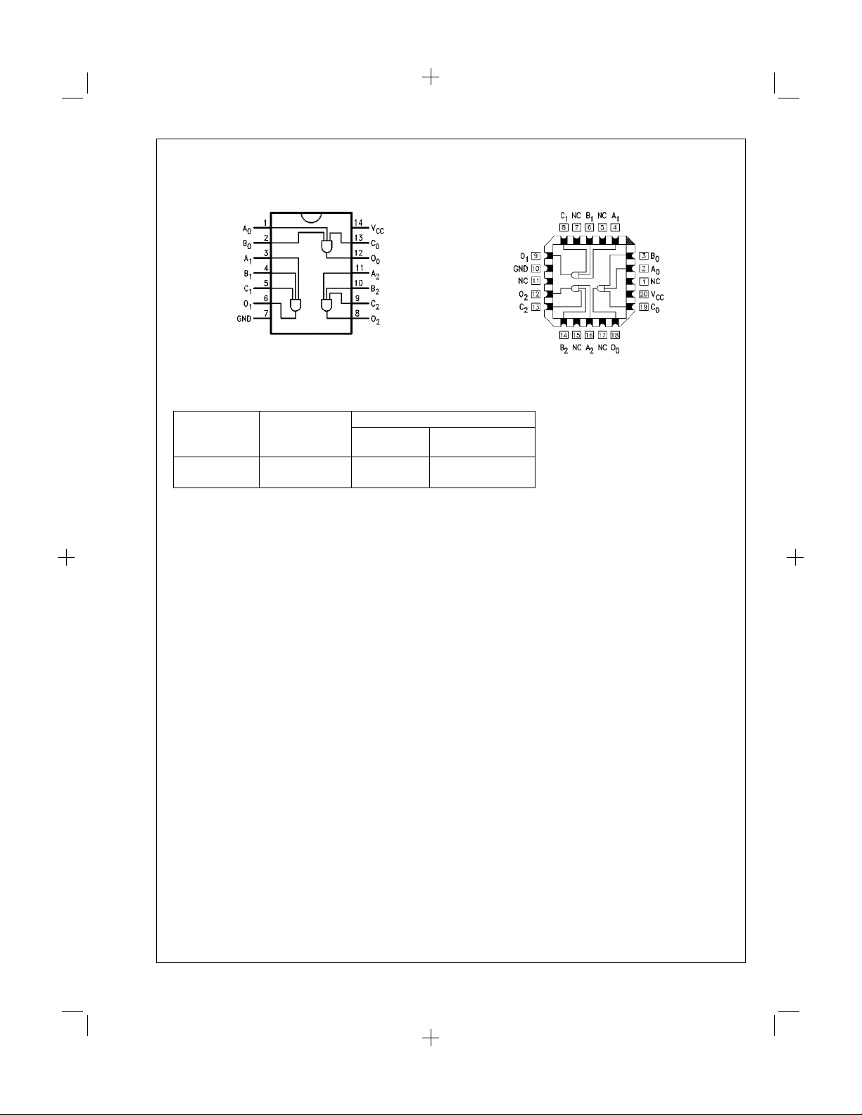
Connection Diagrams
Pin Assignment for
DIP, SOIC and Flatpak
DS009459-2
Unit Loading/Fan Out
See Section 0 for U.L. definitions
54F/74F
Pin Names Description U.L. Input I
HIGH/LOW Output IOH/I
An,Bn,C
O
n
n
Inputs 1.0/1.0 20 µA/−0.6 mA
Outputs 50/33.3 −1 mA/20 mA
Pin Assignment
for LCC
DS009459-1
DSXXX
IH/IIL
OL
www.national.com 2
PrintDate=1997/08/26 PrintTime=16:09:25 9520 ds009459 Rev. No. 1 cmserv Proof 2
Page 3
Absolute Maximum Ratings (Note 3)
If Military/Aerospace specified devices are required,
Current Applied to Output
in LOW State (Max) twice the rated I
please contact the National Semiconductor Sales Office/
Distributors for availability and specifications.
Storage Temperature −65˚C to +150˚C
Ambient Temperature under Bias −55˚C to +125˚C
Junction Temperature under Bias −55˚C to +175˚C
Plastic −55˚C to +150˚C
Pin Potential to
V
CC
Ground Pin −0.5V to +7.0V
Input Voltage (Note 4) −0.5V to +7.0V
Input Current (Note 4) −30 mA to +5.0 mA
Voltage Applied to Output
=
in HIGH State (with V
0V)
CC
Standard Output −0.5V to V
Recommended Operating
Conditions
Free Air Ambient Temperature
Military −55˚C to +125˚C
Commercial 0˚C to +70˚C
Supply Voltage
Military +4.5V to +5.5V
Commercial +4.5V to +5.5V
Note 3: Absolute maximum ratings are values beyond which the device may
be damaged or have its useful life impaired. Functional operation under these
conditions is not implied.
Note 4: Either voltage limit or current limit is sufficient to protect inputs.
CC
TRI-STATE®Output −0.5V to +5.5V
DC Electrical Characteristics
Symbol Parameter 54F/74F Units V
Min Typ Max
V
IH
V
IL
V
CD
V
OH
V
OL
I
IH
I
BVI
I
CEX
V
ID
I
OD
I
IL
I
OS
I
CCH
I
CCL
Input HIGH Voltage 2.0 V Recognized as a HIGH Signal
Input LOW Voltage 0.8 V Recognized as a LOW Signal
Input Clamp Diode Voltage −1.2 V Min I
Output HIGH 54F 10%V
Voltage 74F 10%V
74F 5%V
Output LOW 54F 10%V
Voltage 74F 10%V
2.5 I
CC
2.5 V Min I
CC
2.7 I
CC
CC
CC
0.5 V Min I
0.5 I
Input HIGH 54F 20.0 µA Max V
Current 74F 5.0
Input HIGH Current 54F 100 µA Max V
Breakdown Test 74F 7.0
Output HIGH 54F 250 µA Max V
Leakage Current 74F 50
Input Leakage 74F 4.75 V 0.0 I
Test All other pins grounded
Output Leakage 74F 3.75 µA 0.0 V
Circuit Current All other pins grounded
Input LOW Current −0.6 mA Max V
Output Short-Circuit Current −60 −150 mA Max V
Power Supply Current 4.1 6.2 mA Max V
Power Supply Current 6.5 9.7 mA Max V
(mA)
OL
IN
OH
OH
OH
OL
OL
ID
IN
IN
OUT
IOD
IN
OUT
O
O
=
−18 mA
=
−1 mA
=
−1 mA
=
−1 mA
=
20 mA
=
20 mA
=
2.7V
=
7.0V
=
=
1.9 µA
=
=
0.5V
=
=
HIGH
=
LOW
Conditions
V
CC
150 mV
0V
CC
AC Electrical Characteristics
See Section 0 for Waveforms and Load Configurations
74F 54F 74F
=
+25˚C T
T
A
=
Symbol Parameter V
+5.0V C
CC
=
50 pF
C
L
Min Typ Max Min Max Min Max
t
PLH
t
PHL
Propagation Delay 3.0 4.2 5.6 2.5 7.5 3.0 6.6 ns
An,Bn,Cnto O
n
2.5 4.1 5.5 2.0 7.5 2.5 6.5
3 www.national.com
PrintDate=1997/08/26 PrintTime=16:09:27 9520 ds009459 Rev. No. 1 cmserv Proof 3
=
A,VCC
Mil T
=
50 pF C
L
=
A,VCC
Com Fig.
=
50 pF Units No.
L
kk-kk
DSXXX
DSXXX
Book
Extract
End
Page 4

THIS PAGE IS IGNORED IN THE DATABOOK
4
PrintDate=1997/08/26 PrintTime=16:09:28 9520 ds009459 Rev. No. 1 cmserv Proof 4
Page 5

Ordering Information
The device number is used to form part of a simplified purchasing code where the package type and temperature range are defined as follows:
DS009459-4
Physical Dimensions inches (millimeters) unless otherwise noted
20-Lead Ceramic Leadless Chip Carrier (L)
NS Package Number E20A
5 www.national.com
PrintDate=1997/08/26 PrintTime=16:09:28 9520 ds009459 Rev. No. 1 cmserv Proof 5
Page 6

Physical Dimensions inches (millimeters) unless otherwise noted (Continued)
14-Lead Ceramic Dual-In-Line Package (D)
NS Package Number J14A
14-Lead (0.150" Wide) Molded Small Outline, JEDEC (S)
www.national.com 6
NS Package Number M14A
PrintDate=1997/08/26 PrintTime=16:09:29 9520 ds009459 Rev. No. 1 cmserv Proof 6
Page 7

Physical Dimensions inches (millimeters) unless otherwise noted (Continued)
14-Lead (0.300" Wide) Molded Small Outline, EIAJ (SJ)
14-Lead (0.300" Wide) Molded Dual-In-Line Package (P)
NS Package Number M14D
NS Package Number N14A
7 www.national.com
PrintDate=1997/08/26 PrintTime=16:09:30 9520 ds009459 Rev. No. 1 cmserv
7
Proof 7
Page 8

Physical Dimensions inches (millimeters) unless otherwise noted (Continued)
54F/74F11 Triple 3-Input AND Gate
14-Lead Ceramic Flatpak (F)
NS Package Number W14B
LIFE SUPPORT POLICY
NATIONAL’S PRODUCTS ARE NOT AUTHORIZED FOR USE AS CRITICAL COMPONENTS IN LIFE SUPPORT DEVICES OR SYSTEMS WITHOUT THE EXPRESS WRITTEN APPROVAL OF THE PRESIDENT OF NATIONAL SEMICONDUCTOR CORPORATION. As used herein:
1. Life support devices or systems are devices or sys-
tems which, (a) are intended for surgical implant into
the body, or (b) support or sustain life, and whose failure to perform when properly used in accordance
2. A critical component in any componentof a life support
device or system whose failure to perform can be reasonably expected to cause the failure ofthe lifesupport
device or system, or to affect its safety or effectiveness.
with instructions for use provided in the labeling, can
be reasonably expected to result in a significant injury
to the user.
National Semiconductor
Corporation
Americas
Tel: 1-800-272-9959
Fax: 1-800-737-7018
Email: support@nsc.com
www.national.com
National does not assume any responsibility for use of any circuitry described, no circuit patent licenses are implied and National reserves the right at any time without notice to change said circuitry and specifications.
National Semiconductor
Europe
Fax: +49 (0) 1 80-530 85 86
Email: europe.support@nsc.com
Deutsch Tel: +49 (0) 1 80-530 85 85
English Tel: +49 (0) 1 80-532 78 32
Français Tel: +49 (0) 1 80-532 93 58
Italiano Tel: +49 (0) 1 80-534 16 80
National Semiconductor
Hong Kong Ltd.
13th Floor, Straight Block,
Ocean Centre, 5 Canton Rd.
Tsimshatsui, Kowloon
Hong Kong
Tel: (852) 2737-1600
Fax: (852) 2736-9960
National Semiconductor
Japan Ltd.
Tel: 81-3-5620-6175
Fax: 81-3-5620-6179
PrintDate=1997/08/26 PrintTime=16:09:31 9520 ds009459 Rev. No. 1 cmserv Proof 8
 Loading...