

Datasheet 5962R9160301VFA, 5962R9160301VEA, 5962R9160301V2A, 5962R9160301MFA, 5962R9160301MEA Datasheet (NSC)
...Page 1

54AC169•54ACT169
4-Stage Synchronous Bidirectional Counter
General Description
The ’AC/’ACT169 is fully synchronous 4-stage up/down
counter. The ’AC/’ACT169 is a modulo-16 binary counter. It
features a preset capability for programmable operation,
carry lookahead for easy cascading and a U/D input to control the direction of counting. All state changes, whether in
counting or parallel loading, are initiated by the
LOW-to-HIGH transition of the Clock.
Features
n ICCreduced by 50
%
n Synchronous counting and loading
n Built-In lookahead carry capability
n Presettable for programmable operation
n Outputs source/sink 24 mA
n ’ACT has TTL-compatible inputs
n Standard Microcircuit Drawing (SMD)
5962-91603
Logic Symbols
Pin
Names
Description
CEP
Count Enable Parallel Input
CET
Count Enable Trickle Input
CP Clock Pulse Input
P
0–P3
Parallel Data Inputs
PE
Parallel Enable Input
U/D
Up-Down Count Control Input
Q
0–Q3
Flip-Flop Outputs
TC
Terminal Count Output
FACT™is a trademark of Fairchild Semiconductor Corporation.
DS100276-1
IEEE/IEC
DS100276-2
July 1998
54AC169
•
54ACT169 4-Stage Synchronous Bidirectional Counter
© 1998 National Semiconductor Corporation DS100276 www.national.com
Page 2
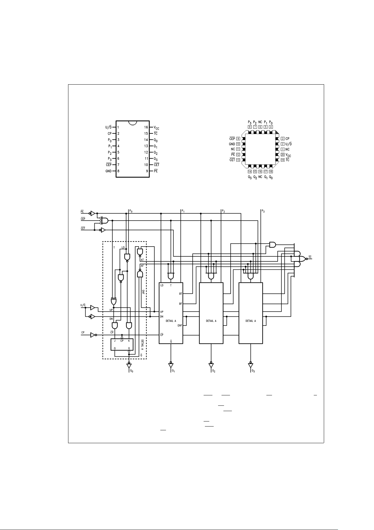
Connection Diagrams
Logic Diagram
Functional Description
The ’AC/’ACT169 uses edge-triggered J-K-type flip-flops
and have no constraints on changing the control or data input signals in either state of the Clock. The only requirement
is that the various inputs attain the desired state at least a
setup time before the rising edge of the clock and remain
valid for the recommended hold time thereafter. The parallel
load operation takes precedence over the other operations,
as indicated in the Mode Select Table.When PE is LOW, the
data on the P0–P3inputs enters the flip-flops on the next rising edge of the Clock. In order for counting to occur, both
CEP and CET must be LOW and PE must be HIGH; the U/D
input then determines the direction of counting. The Terminal
Count (TC) output is normally HIGH and goes LOW, provided that CET is LOW, when a counter reaches zero in the
Count Down mode or reaches 15 in the Count Up mode. The
TC output state is not a function of the Count Enable Parallel
(CEP) input level. If an illegal state occurs, the ’AC169 will
return to the legitimate sequence within two counts. Since
Pin Assignment
for DIP and Flatpak
DS100276-3
Pin Assignment
for LCC
DS100276-4
DS100276-5
Please note that this diagram is provided only for the understanding of logic operations and should not be used to estimate propagation delays.
www.national.com 2
Page 3

Functional Description (Continued)
the TC signal is derived by decoding the flip-flop states,
there exists the possibility of decoding spikes on TC. For this
reason the use of TC as a clock signal is not recommended
(see logic equations below).
1. Count Enable=CEP
•
CET•PE
2. Up: TC=Q
0
•
Q
1
•
Q2Q
3
•
(Up)•CET
3. Down: TC=Q
0
•
Q
1
•
Q
2
•
Q
3
•
(Down)•CET
Mode Select Table
PE CEP CET U/D Action on Rising
Clock Edge
L X X X Load (P
n
to Qn)
H L L H Count Up (Increment)
H L L L Count Down (Decrement)
H H X X No Change (Hold)
H X H X No Change (Hold)
H=HIGH Voltage Level
L=LOW Voltage Level
X=Immaterial
State Diagrams
DS100276-6
3 www.national.com
Page 4

Absolute Maximum Ratings (Note 1)
If Military/Aerospace specified devices are required,
please contact the National Semiconductor Sales Office/
Distributors for availability and specifications.
Supply Voltage (V
CC
) −0.5V to +7.0V
DC Input Diode Current (I
IK
)
V
I
=
−0.5V −20 mA
V
I
=
V
CC
+ 0.5V +20 mA
DC Input Voltage (V
I
) −0.5V to VCC+ 0.5V
DC Output Diode Current (I
OK
)
V
O
=
−0.5V −20 mA
V
O
=
V
CC
+ 0.5V +20 mA
DC Output Voltage (V
O
) −0.5V to VCC+ 0.5V
DC Output Source
or Sink Current (I
O
)
±
50 mA
DC V
CC
or Ground Current
per Output Pin (I
CC
or I
GND
)
±
50 mA
Storage Temperature (T
STG
) −65˚C to +150˚C
Junction Temperature (T
J
)
CDIP 175˚C
Recommended Operating
Conditions
Supply Voltage (VCC)
’AC 2.0V to 6.0V
’ACT 4.5V to 5.5V
Input Voltage (V
I
) 0VtoV
CC
Output Voltage (VO) 0VtoV
CC
Operating Temperature (TA)
54AC/ACT −55˚C to +125˚C
Minimum Input Edge Rate (∆V/∆t)
’AC Devices
V
IN
from 30%to 70%of V
CC
V
CC
@
3.3V, 4.5V, 5.5V 125 mV/ns
Minimum Input Edge Rate (∆V/∆t)
’ACT Devices
V
IN
from 0.8V to 2.0V
V
CC
@
4.5V, 5.5V 125 mV/ns
Note 1: Absolute maximum ratings are those values beyond which damage
to the device may occur. The databook specifications should be met, without
exception, to ensure that the system design is reliable over its power supply,
temperature, and output/input loading variables. National does not recommend operation of FACT
™
circuits outside databook specifications.
DC Characteristics for ’AC Family Devices
54AC
Symbol Parameter V
CC
T
A
=
Units Conditions
(V) −55˚C to +125˚C
Guaranteed
Limits
V
IH
Minimum High Level 3.0 2.1 V
OUT
=
0.1V
Input Voltage 4.5 3.15 V or V
CC
− 0.1V
5.5 3.85
V
IL
Maximum Low Level 3.0 0.9 V
OUT
=
0.1V
Input Voltage 4.5 1.35 V or V
CC
− 0.1V
5.5 1.65
V
OH
Minimum High Level 3.0 2.9 I
OUT
=
−50 µA
Output Voltage 4.5 4.4 V
5.5 5.4
(Note 2)
V
IN
=
V
IL
or V
IH
3.0 2.4 IOH= −12 mA
4.5 3.7 V I
OH
= −24 mA
5.5 4.7 I
OH
= −24 mA
V
OL
Maximum Low Level 3.0 0.1 I
OUT
=
50 µA
Output Voltage 4.5 0.1 V
5.5 0.1
(Note 2)
V
IN
=
V
IL
or V
IH
3.0 0.50 IOL=12mA
4.5 0.50 V I
OL
=24mA
5.5 0.50 I
OL
=24mA
I
IN
Maximum Input 5.5
±
1.0 µA V
I
=
V
CC
, GND
Leakage Current
www.national.com 4
Page 5

DC Characteristics for ’AC Family Devices (Continued)
54AC
Symbol Parameter V
CC
T
A
=
Units Conditions
(V) −55˚C to +125˚C
Guaranteed
Limits
I
OLD
Minimum Dynamic
Output Current (Note 3)
5.5 50 mA V
OLD
=
1.65V Max
I
OHD
5.5 −50 mA V
OHD
=
3.85V Min
I
CC
Maximum Quiescent 5.5 80.0 µA V
IN
=
V
CC
Supply Current or GND
Note 2: All outputs loaded; thresholds on input associated with output under test.
Note 3: Maximum test duration 2.0 ms, one output loaded at a time.
Note 4: I
IN
and I
CC
@
3.0V are guaranteed to be less than or equal to the respective limit@5.5V VCC.
I
CC
for 54AC@25˚C is identical to 74AC@25˚C.
DC Characteristics for ’ACT Family Devices
54ACT
Symbol Parameter V
CC
T
A
=
Units Conditions
(V) −55˚C to +125˚C
Guaranteed
Limits
V
IH
Minimum High Level 4.5 2.0 V V
OUT
=
0.1V
Input Voltage 5.5 2.0 or V
CC
− 0.1V
V
IL
Maximum Low Level 4.5 0.8 V V
OUT
=
0.1V
Input Voltage 5.5 0.8 or V
CC
− 0.1V
V
OH
Minimum High Level 4.5 4.4 V I
OUT
=
−50 µA
Output Voltage 5.5 5.4
(Note 5)
V
IN
=
V
IL
or V
IH
4.5 3.70 V IOH= −24 mA
5.5 4.70 I
OH
= −24 mA
V
OL
Maximum Low Level 4.5 0.1 V I
OUT
=
50 µA
Output Voltage 5.5 0.1
(Note 5)
V
IN
=
V
IL
or V
IH
4.5 0.50 V IOL=24mA
5.5 0.50 I
OL
=24mA
I
IN
Maximum Input 5.5
±
1.0 µA V
I
=
V
CC
, GND
Leakage Current
I
CCT
Maximum 5.5 1.6 mA V
I
=
V
CC
− 2.1V
I
CC
/Input
I
OLD
Minimum Dynamic
Output Current (Note 6)
5.5 50 mA V
OLD
=
1.65V Max
I
OHD
5.5 −50 mA V
OHD
=
3.85V Min
I
CC
Maximum Quiescent 5.5 80.0 µA V
IN
=
V
CC
Supply Current or GND
Note 5: All outputs loaded; thresholds on input associated with output under test.
Note 6: Maximum test duration 2.0 ms, one output loaded at a time.
Note 7: I
CC
for 54ACT@25˚C is identical to 74ACT@25˚C.
5 www.national.com
Page 6

AC Electrical Characteristics
54AC
V
CC
T
A
=
−55˚C Fig.
Symbol Parameter (V) to +125˚C Units No.
(Note 8) C
L
=
50 pF
Min Max
f
max
Maximum Clock 3.3 55 MHz
Frequency 5.0 75
t
PLH
Propagation Delay 3.3 1.0 15.0
CP to Q
n
5.0 1.5 12.0 ns
(PE HIGH or LOW)
t
PHL
Propagation Delay 3.3 1.0 16.5
CP to Q
n
5.0 1.5 13.0 ns
(PE HIGH or LOW)
t
PLH
Propagation Delay 3.3 3.0 22.0 ns
CP to TC
5.0 3.0 16.0
t
PHL
Propagation Delay 3.3 3.0 22.0 ns
CP to TC
5.0 3.0 16.0
t
PLH
Propagation Delay 3.3 1.0 18.5 ns
CET to TC
5.0 1.5 13.0
t
PHL
Propagation Delay 3.3 1.0 16.0 ns
CET to TC
5.0 1.5 11.0
t
PLH
Propagation Delay 3.3 1.0 18.5 ns
U/D to TC
5.0 1.5 13.0
t
PHL
Propagation Delay 3.3 1.0 16.5 ns
U/D to TC
5.0 1.5 12.0
Note 8: Voltage Range 3.3 is 3.3V±0.3V
Voltage Range 5.0 is 5.0V
±
0.5V
AC Operating Requirements
54AC
V
CC
T
A
=
−55˚C Fig.
Symbol Parameter (V) to +125˚C Units No.
(Note 9) C
L
=
50 pF
Guaranteed
Minimum
t
s
Setup Time, 3.3 7.0
HIGH or LOW 5.0 4.5 ns
P
n
to CP
t
h
Hold Time, HIGH or LOW 3.3 2.0 ns
P
n
to CP 5.0 2.5
t
s
Setup Time, 3.3 13.5
HIGH or LOW 5.0 9.0 ns
CEP to CP
t
h
Hold Time, HIGH or LOW 3.3 0.5 ns
CEP to CP
5.0 2.5
t
s
Setup Time, 3.3 13.5
HIGH or LOW 5.0 9.0 ns
CET to CP
www.national.com 6
Page 7

AC Operating Requirements (Continued)
54AC
V
CC
T
A
=
−55˚C Fig.
Symbol Parameter (V) to +125˚C Units No.
(Note 9) C
L
=
50 pF
Guaranteed
Minimum
t
h
Hold Time, HIGH or LOW 3.3 0.5 ns
CET to CP
5.0 2.5
t
s
Setup Time, 3.3 8.5
HIGH or LOW 5.0 6.5 ns
PE to CP
t
h
Hold Time, HIGH or LOW 3.3 0.5 ns
PE to CP
5.0 2.0
t
s
Setup Time, 3.3 13.0
HIGH or LOW 5.0 9.0 ns
U/D to CP
t
h
Hold Time, HIGH or LOW 3.3 0.5 ns
U/D to CP
5.0 2.0
t
w
CP Pulse Width, 3.3 5.0 ns
HIGH or LOW 5.0 5.0
Note 9: Voltage Range 3.3 is 3.3V±0.3V
Voltage Range 5.0 is 5.0V
±
0.5V
AC Electrical Characteristics
54ACT
V
CC
T
A
=
−55˚C Fig.
Symbol Parameter (V) to +125˚C Units No.
(Note 10) C
L
=
50 pF
Min Max
f
max
Maximum Clock 5.0 75 MHz
Frequency
t
PLH
Propagation Delay
CP to Q
n
5.0 1.5 12.5 ns
(PE HIGH or LOW)
t
PHL
Propagation Delay
CP to Q
n
5.0 1.5 12.5 ns
(PE HIGH or LOW)
t
PLH
Propagation Delay 5.0 1.5 16.5 ns
CP to TC
t
PHL
Propagation Delay 5.0 1.5 16.5 ns
CP to TC
t
PLH
Propagation Delay 5.0 1.5 13.5 ns
CET to TC
t
PHL
Propagation Delay 5.0 1.5 13.5 ns
CET to TC
t
PLH
Propagation Delay 5.0 1.5 14.5 ns
U/D to TC
t
PHL
Propagation Delay 5.0 1.5 14.5 ns
U/D to TC
7 www.national.com
Page 8

AC Electrical Characteristics (Continued)
Note 10: Voltage Range 5.0 is 5.0V±0.5V
AC Operating Requirements
54ACT
V
CC
T
A
=
−55˚C Fig.
Symbol Parameter (V) to +125˚C Units No.
(Note 11) C
L
=
50 pF
Guaranteed
Minimum
t
s
Setup Time,
HIGH or LOW 5.0 4.5 ns
P
n
to CP
t
h
Hold Time, HIGH or LOW 5.0 2.5 ns
P
n
to CP
t
s
Setup Time,
HIGH or LOW 5.0 9.0 ns
CEP to CP
t
h
Hold Time, HIGH or LOW 5.0 2.5 ns
CEP to CP
t
s
Setup Time,
HIGH or LOW 5.0 9.0 ns
CET to CP
t
h
Hold Time, HIGH or LOW 5.0 2.5 ns
CET to CP
t
s
Setup Time,
HIGH or LOW 5.0 6.5 ns
PE to CP
t
h
Hold Time, HIGH or LOW 5.0 2.0 ns
PE to CP
t
s
Setup Time,
HIGH or LOW 5.0 9.0 ns
U/D to CP
t
h
Hold Time, HIGH or LOW 5.0 2.0 ns
U/D to CP
t
w
CP Pulse Width, 5.0 5.0 ns
HIGH or LOW
Note 11: Voltage Range 5.0 is 5.0V±0.5V
Capacitance
Symbol Parameter Typ Units Conditions
C
IN
Input Capacitance 4.5 pF V
CC
=
Open
C
PD
Power Dissipation 60.0 pF V
CC
=
5.0V
Capacitance
www.national.com 8
Page 9

Physical Dimensions inches (millimeters) unless otherwise noted
20-Terminal Ceramic Leadless Chip Carrier (L)
NS Package Number E20A
16-Lead Ceramic Dual-In-Line Package (D)
NS Package Number J16A
9 www.national.com
Page 10

Physical Dimensions inches (millimeters) unless otherwise noted (Continued)
LIFE SUPPORT POLICY
NATIONAL’S PRODUCTS ARE NOT AUTHORIZED FOR USE AS CRITICAL COMPONENTS IN LIFE SUPPORT DEVICES OR SYSTEMS WITHOUT THE EXPRESS WRITTEN APPROVAL OF THE PRESIDENT OF NATIONAL SEMICONDUCTOR CORPORATION. As used herein:
1. Life support devices or systems are devices or systems which, (a) are intended for surgical implant into
the body, or (b) support or sustain life, and whose failure to perform when properly used in accordance
with instructions for use provided in the labeling, can
be reasonably expected to result in a significant injury
to the user.
2. A critical component in any component of a life support
device or system whose failure to perform can be reasonably expected to cause the failure of the life support
device or system, or to affect its safety or effectiveness.
National Semiconductor
Corporation
Americas
Tel: 1-800-272-9959
Fax: 1-800-737-7018
Email: support@nsc.com
www.national.com
National Semiconductor
Europe
Fax: +49 (0) 1 80-530 85 86
Email: europe.support@nsc.com
Deutsch Tel: +49 (0) 1 80-530 85 85
English Tel: +49 (0) 1 80-532 78 32
Français Tel: +49 (0) 1 80-532 93 58
Italiano Tel: +49 (0) 1 80-534 16 80
National Semiconductor
Asia Pacific Customer
Response Group
Tel: 65-2544466
Fax: 65-2504466
Email: sea.support@nsc.com
National Semiconductor
Japan Ltd.
Tel: 81-3-5620-6175
Fax: 81-3-5620-6179
16-Lead Ceramic Flatpak (F)
NS Package Number W16A
54AC169
•
54ACT169 4-Stage Synchronous Bidirectional Counter
National does not assume any responsibility for use of any circuitry described, no circuit patent licenses are implied and National reserves the right at any time without notice to change said circuitry and specifications.
 Loading...