

Page 1
PRELIMINARY DATA SHEET
53246
40VDC – 2A SOLID STATE RELAY
RADIATION TOLERANT
Mii
HYBRID MICROELECTRONICS
PRODUCTS DIVISION
Features:
This Design Tested to 100 krad (Si) Total Dose
•
Hermetically Sealed in Surface Mount Package
•
Low On-resistance
•
2A Continuous Output Current
•
Operation over Full Military Temperature
•
Range -55°C to +125°C
Optically Coupled
•
Input/Output Isolation Tested to 1000 VDC
•
Shock and Vibration Resistance
•
DESCRIPTION
Applications:
Satellite/Space Systems
•
Military/High Reliability Systems
•
Power Distribution/Switching
•
Solenoid Driver
•
Stepper Motor Driver
•
Switching Heaters
•
The 53246 is a SPST, radiation tolerant, DC solid-state relay (SSR) designed for military and space applications.
This light-weight device is resistant to damage from severe shock and vibration, and is immune to contact related
problems inherent in electro-mechanical relays. The SSR is enclosed in a hermetic metal package to ensure
reliability in harsh environments. Effective isolation of 1000 VDC between control and load circuits is achieved
through the use of optical coupling.
Functionally, the device operates as a single-pole single-throw, normally open (1 Form A) DC solid-state relay. The
SSR is actuated by an input current of 5 to 15 mA, which can be supplied from standard logic types such as a
standard TTL device. Output is provided by a power MOSFET exhibiting very low R
and capable of carrying a
DS(ON)
continuous current of 2 amperes. This design has demonstrated it will function with minimal degradation after
exposure to 100 krad (Si) total dose. The 53246 is available in a variety of quality levels from COTS to class K
including any custom screening requirements. The basic data sheet part is environmentally screened to H level in
accordance with Table C-IX of MIL-PRF-38534.
ABSOLUTE MAXIMUM RATINGS
Output Voltage ....................................................................................................................................................... 50 VDC
Continuous Output current ............................................................................................................................................2 A
Peak Output Current
(1)
........................................................................................................................................19 A
Storage Temperature Range ..................................................................................................................-65°C to +150°C
Operating Junction Temperature ............................................................................................................-55°C to +150°C
Lead Solder Temperature, for 10 seconds .............................................................................................................300°C
Continuous Input Current .........................................................................................................................................20 mA
Peak Input Current
Reverse Input Voltage ............................................................................................................................................. 6 VDC
Power Dissipation
(2)
............................................................................................................................................. 100 mA
(3)
...................................................................................................................................................20 W
Linear Derating Factor ....................................................................................................................................... 0.15 W/°C
WEIGHT: 3.7 grams (typical
Micropac Industries cannot assume any responsibility for any circuits shown or represent that they are free from patent infringement. Micropac
MICROPAC INDUSTRIES, INC. HYBRID MICROELECTRONICS PRODUCTS DIVISION • 905 E. Walnut St., Garland, TX 75040 • (972) 272-3571 • Fax (972) 494-2281
reserves the right to make changes at any time in order to improve design and to supply the best product possible.
www.micropac.com E-MAIL: [email protected]
01/30/01
Page 2
Preliminary Data Sheet
53246
Radiation Tolerant 40VDC – 2A Solid State Relay
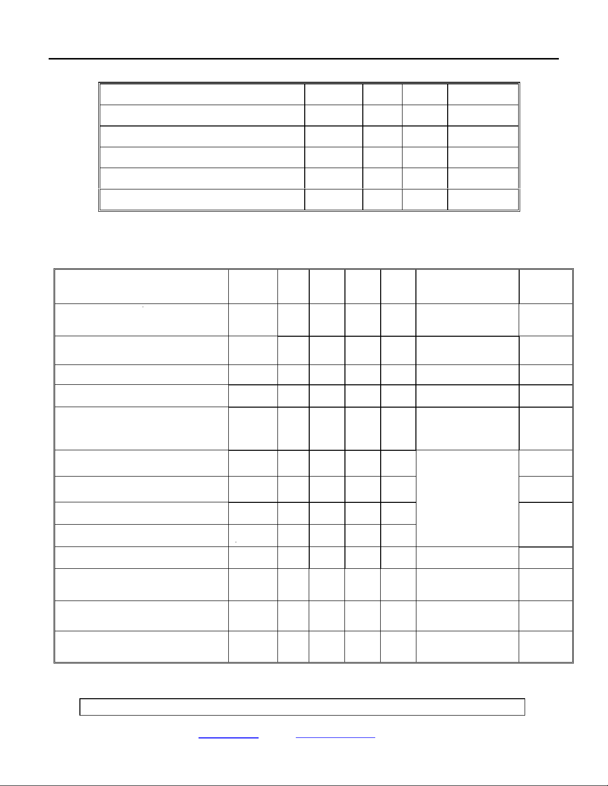
RECOMMENDED OPERATING CONDITIONS:
Parameter Symbol Min. Max. Units
Output Voltage V
Continuous Output Current I
Input Current (on) I
Input Voltage (off) V
Operating Case Temperature T
ELECTRICAL SPECIFICATIONS (Pre-Irradiation)
= -55°C to +125°C unless otherwise specified
T
C
Parameter Symbol Min. Typ.* Max. Unit
Output On-Resistance R
Output Leakage Current I
Input Forward Voltage V
Input Reverse Breakdown Voltage V
(ON)
O (OFF)
F
R
O (OFF)
O (ON)
F (ON)
F (OFF)
C
515 mA
01 VDC
-55 125 °C
40 VDC
2A
Test Conditions Notes
s
= 15 mA
I
.032 .060
250
1
<
µ
F
Ω
A
= 1 A
I
O
= 1 VDC
V
F
V
= 50 VDC
O
3.10 3.75 4.20 VDC IF = 15 mA
640
VDC
I
= 10 µA
R
Input-Output Leakage I
Turn-On Time t
Turn-Off time t
Rise Time t
Fall Time t
Thermal Resistance (junction-case)
Output Off-Capacitance C
Input Capacitance C
Input-Output Capacitance C
* All typical values are at TC = 25°C
Micropac Industries cannot assume any responsibility for any circuits shown or represent that they are free from patent infringement. Micropac
reserves the right to make changes at any time in order to improve design and to supply the best product possible.
I-O
ON
OFF
R
F
θ
JC
O (OFF)
IN
I-O
2.8 8.0 ms
61 80 ms
2.1 6.0 ms
31 50 ms
5.5
1.8
27
3.8
RH ≤ 45%, t = 5 s
1
A
V
µ
= 1000 VDC
I-O
= 25°C
T
C
4, 5
Figures
I
= 15 mA
F
= 10 A
I
O
V load = 40 VDC
Pulse width = 10 ms
Duty cycle ≤ 1%
3, 4
Figures
3, 5
6,
Figure 3
°C/W
= 28 VDC
V
nF
pF
pF
O
f = 1 MHz
= 0 V
V
F
f = 1 MHz
= 0 V
V
I-O
f = 1 MHz
4
MICROPAC INDUSTRIES, INC. HYBRID MICROELECTRONICS PRODUCTS DIVISION • 905 E. Walnut St., Garland, TX 75040 • (972) 272-3571 • Fax (972) 494-2281
www.micropac.com E-MAIL: [email protected]
01/30/01
Page 3
Preliminary Data Sheet
Radiation Tolerant 40VDC - 2A Solid State Relay
Notes:
53246
1. Non-repetitive, pulse width
2. Non-repetitive, pulse width
3. Case Temperature T
= 25°C (see Figure 7).
C
10 ms, T
≤
100 µs, T
≤
= 25°C (see Figure 6).
C
= 25°C.
C
4. Input pins shorted together and output pins shorted together.
5. Input-output potential applied momentarily, not an operating condition.
6. Rise time is measured from 10% to 90% of load current (90% to 10% of V
10% of load current (10% to 90% of V
).
O
). Fall time is measured from 90% to
O
CAUTION:
Care should be taken so as not to exceed the maximum power dissipation and maximum junction temperature
when repetitively switching loads.
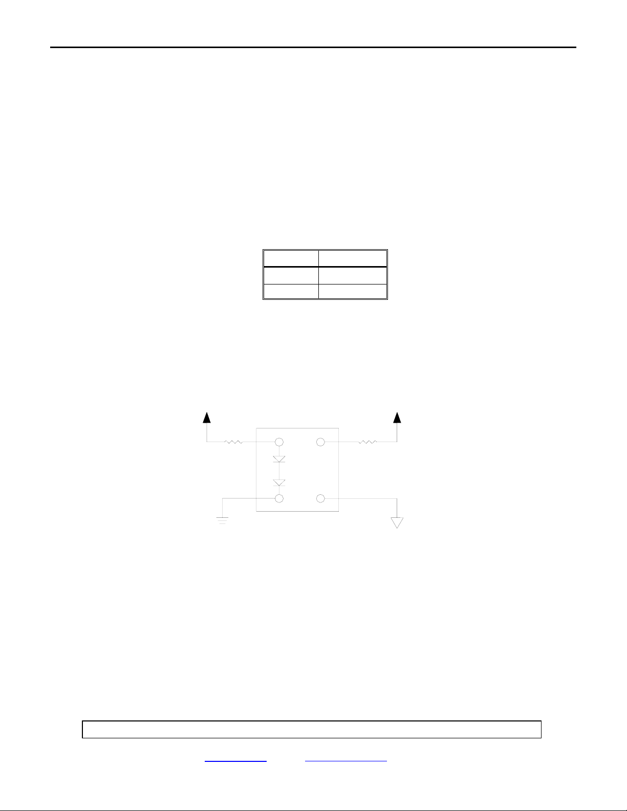
INPUT OUTPUT
ON ON
OFF OFF
Figure 1. Truth Table
Figure 1. Terminal Connections
+V
-V
C
R
S
C
4
1
3
2
+DC SUPPLY
R
LOAD
OUTPUT GND
TOP VIEW
Figure 2. Terminal Connections
Micropac Industries cannot assume any responsibility for any circuits shown or represent that they are free from patent infringement. Micropac
MICROPAC INDUSTRIES, INC. HYBRID MICROELECTRONICS PRODUCTS DIVISION • 905 E. Walnut St., Garland, TX 75040 • (972) 272-3571 • Fax (972) 494-2281
reserves the right to make changes at any time in order to improve design and to supply the best product possible.
www.micropac.com E-MAIL: [email protected]
01/30/01
Page 4
Preliminary Data Sheet
53246
Radiation Tolerant 40VDC – 2A Solid State Relay
Z = 50
O
t = t = 10ns
R
F
(100mV/mA)
PULSE
GENERATOR
I
F
MONITOR
I
V
V = 40 V
LOAD
R = 20
L
MONITOR
= 25 pF
L
V
O
1
2
100
50%
F
O
10%
4
C
(INCLUDES PROBE AND
FIXTURE CAPACITANCE)
3
50%
90%
t
t
ON
OFF
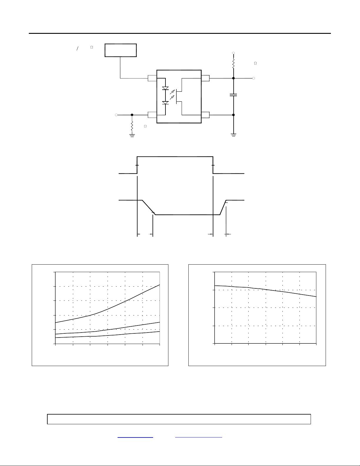
Figure 3. Switching Waveforms and Test Circuits
25
20
80
60
15
5mA
40
10
Turn-on Time (m s )
5
15mA
0
-55-25 5 35 65 95125
Temperature (°C)
10mA
20
Turn-off Time (ms)
0
-55 -25 5 35 65 95 125
Temperature (°C)
Figure 4. Turn-on Time vs. Case Temperature Figure 5. Turn-off Time vs. Case Temperature
for Different Values of I
(typical data).
F
with IF = 5 to 15mA (typical data).
Micropac Industries cannot assume any responsibility for any circuits shown or represent that they are free from patent infringement. Micropac
MICROPAC INDUSTRIES, INC. HYBRID MICROELECTRONICS PRODUCTS DIVISION • 905 E. Walnut St., Garland, TX 75040 • (972) 272-3571 • Fax (972) 494-2281
reserves the right to make changes at any time in order to improve design and to supply the best product possible.
www.micropac.com E-MAIL: [email protected]
01/30/01
Page 5
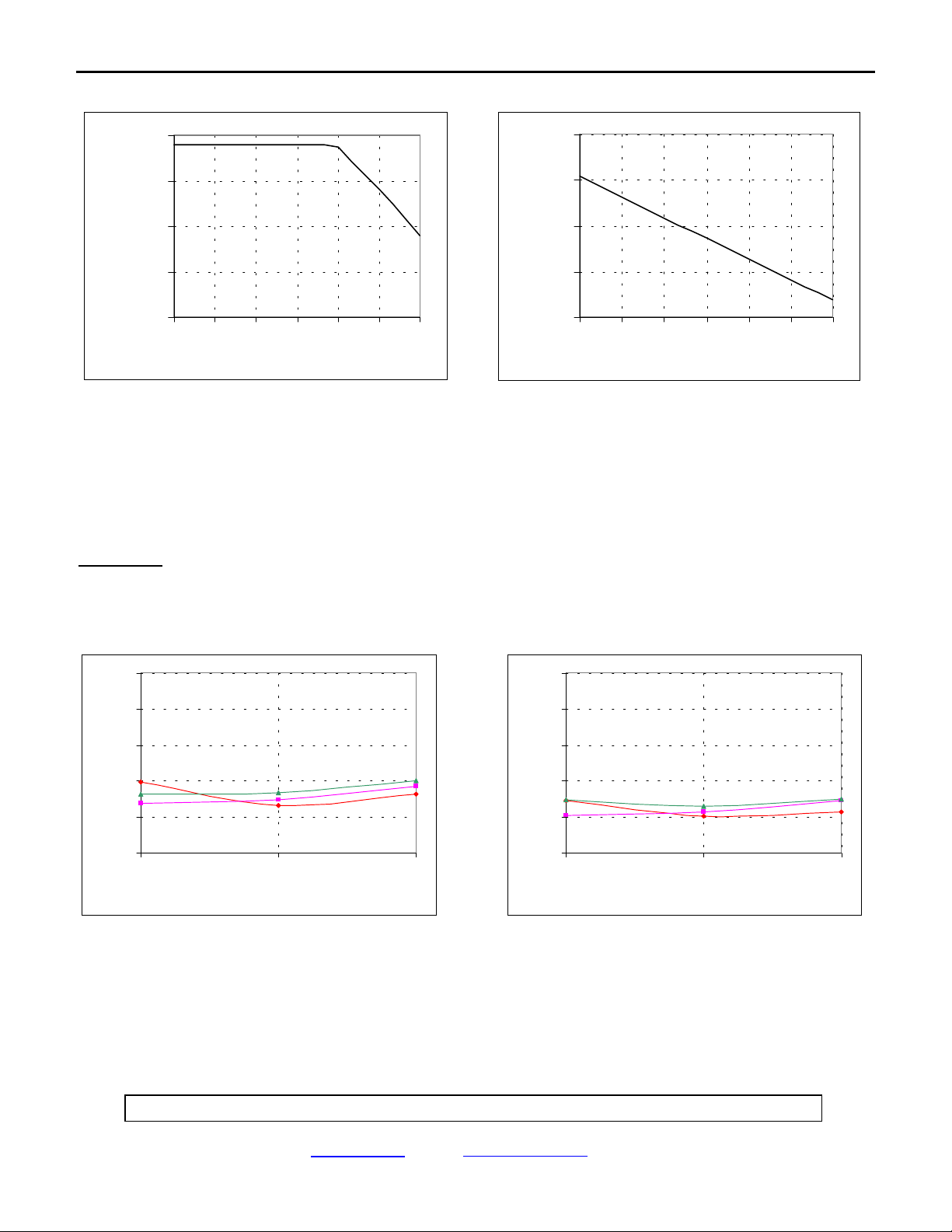
Preliminary Data Sheet 53246
Radiation Tolerant 40VDC - 2A Solid State Relay
20
15
10
Current (A)
5
Maximum Peak Output
0
-55 -25 5 35 65 95 125
Temperature (°C)
Figure 6. Maximum Non-repetitive Output Current Figure 7. Maximum Average Output Power
vs. Case Temperature (pulse width
10 ms). Dissipation vs. Case Temperature.
≤
40
30
20
Dissipation (W)
10
Maximum Average Power
0
-55 -25 5 35 65 95 125
Temperature (°C)
TOTAL DOSE TEST RESULTS
Disclaimer: The data of 3 representative units irradiated in Cobalt-60 chamber is only typical of one lot of
solid state relays. Micropac does not guarantee performance of its SSR to these radiation levels. Individual
lots have to be screened to guarantee the performance.
10
8
6
4
Turn-On Time, ms
2
0
050100
Total Dose, krad (Si)
Figure 8. Turn-On Time vs Total Dose Figure 9. Rise Time vs Total Dose
at V
I
Micropac Industries cannot assume any responsibility for any circuits shown or represent that they are free from patent infringement. Micropac
= 28 V, R
out
= 15 mA, 10% duty cycle. Iin = 15 mA, 10% duty cycle.
in
reserves the right to make changes at any time in order to improve design and to supply the best product possible.
= 35 Ω, at V
load
10
8
6
4
Rise Time, ms
2
0
050100
Total Dose, krad (Si)
= 28 V, R
out
= 35 Ω,
load
MICROPAC INDUSTRIES, INC. HYBRID MICROELECTRONICS PRODUCTS DIVISION • 905 E. Walnut St., Garland, TX 75040 • (972) 272-3571 • Fax (972) 494-2281
www.micropac.com E-MAIL: [email protected]
01/30/01
Page 6
Preliminary Data Sheet 53246
Radiation Tolerant 40VDC - 2A Solid State Relay
70
40
65
35
60
55
50
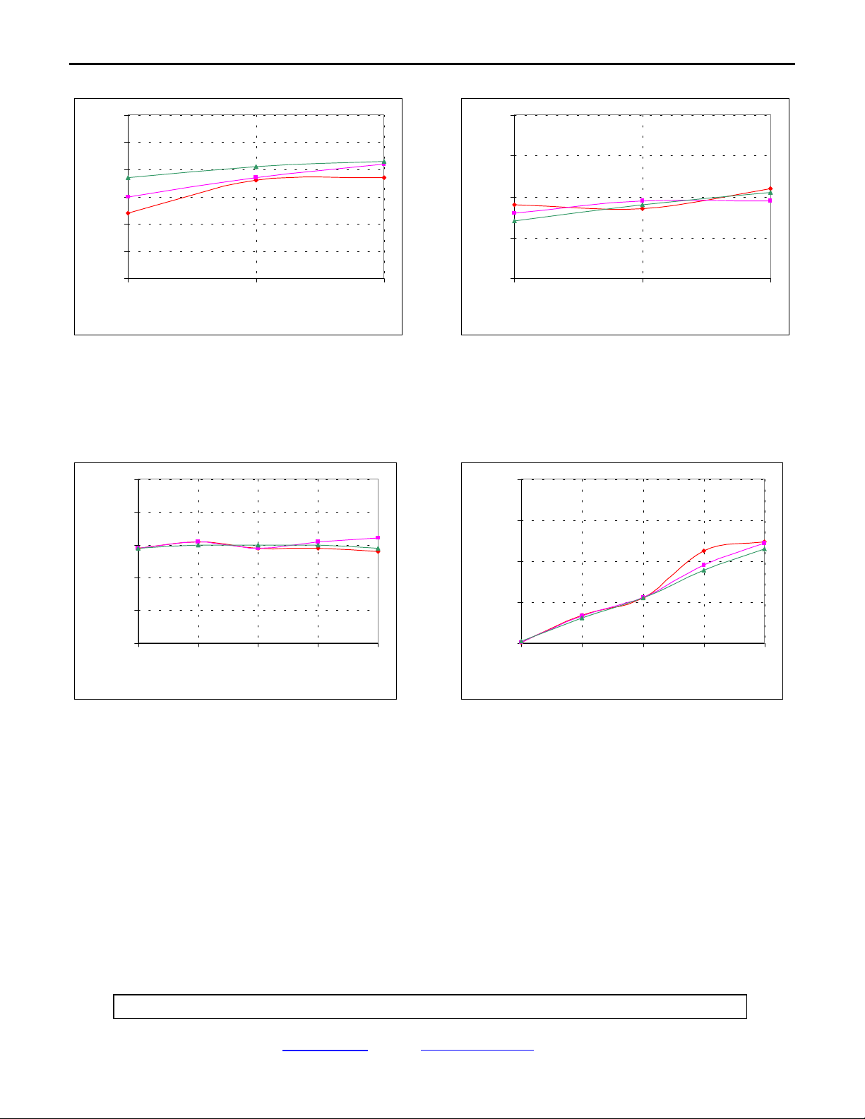
Turn-Off Time, ms
45
40
0 50 100
Total Dose, krad (Si)
Figure 10. Turn-Off Time vs Total Dose Figure 11. Fall Time vs Total Dose
at V
I
= 28 V, R
out
= 15 mA, 10% duty cycle. Iin = 15 mA, 10% duty cycle
in
= 35 Ω, at V
load
0.05
0.04
30
Fall Time, ms
25
20
0 50 100
Total Dose, krad (Si)
= 28 V, R
out
= 35 Ω,
load
100
75
.
0.03
50
0.02
0.01
On-Resistance, ohm
0.00
0255075100
Total Dose, krad (Si)
25
Output Leakage Current, nA
0
0255075100
Total Dose, krad (Si)
Figure 12. On-Resistance vs Total Dose Figure 13. Output Leakage Current vs Total Dose
at I
=10 mA, I
F
=100 mA for 1second. at VF = 1.0 V, V
out
= 50 V.
out
Micropac Industries cannot assume any responsibility for any circuits shown or represent that they are free from patent infringement. Micropac
MICROPAC INDUSTRIES, INC. HYBRID MICROELECTRONICS PRODUCTS DIVISION • 905 E. Walnut St., Garland, TX 75040 • (972) 272-3571 • Fax (972) 494-2281
reserves the right to make changes at any time in order to improve design and to supply the best product possible.
www.micropac.com E-MAIL: [email protected]
01/30/01
Page 7
Preliminary Data Sheet 53246
Radiation Tolerant 40VDC - 2A Solid State Relay
5.0
4.5
4.0
3.5
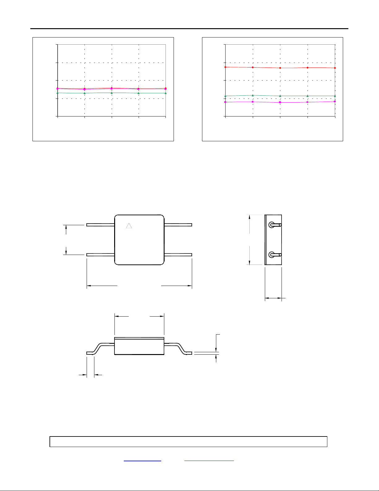
Input Forward Voltage, VDC
3.0
0255075100
Total Dose, krad (Si)
70
60
50
40
Input Reverse Voltage, VDC
30
0 255075100
Total Dose, krad (Si)
Figure 12. Input Forward Voltage vs Total Dose Figure 15. Input Reverse Voltage vs Total Dose
at I
=15 mA. at IR = 10 µA.
F
CASE OUTLINE
.300
1
4
23
1.060 ±.030
.500
.060 (TYP)
.500
.175
.025 ±.002 DIA
(4 PLCS)
Micropac Industries cannot assume any responsibility for any circuits shown or represent that they are free from patent infringement. Micropac
MICROPAC INDUSTRIES, INC. HYBRID MICROELECTRONICS PRODUCTS DIVISION • 905 E. Walnut St., Garland, TX 75040 • (972) 272-3571 • Fax (972) 494-2281
reserves the right to make changes at any time in order to improve design and to supply the best product possible.
www.micropac.com E-MAIL: [email protected]
01/30/01
 Loading...