

Page 1
High Gain Darlington Output
Optocouplers
Technical Data
Features
• High Current Transfer
Ratio–1500% Typical
• Low Input Current
Requirement–0.5 mA
• Performance Guaranteed
over 0°C to 70°C
Temperature Range
• Internal Base-Emitter
Resistor Minimizes Output
Leakage
• Gain-Bandwidth Adjustment
Pin
• Safety Approval
UL Recognized -2500 V rms for
1 Minute
CSA Approved
Applications
• Telephone Ring Detector
• Digital Logic Ground
Isolation
• Low Input Current Line
Receiver
• Line Voltage Status
Indicator–Low Input Power
Dissipation
• Logic to Reed Relay Interface
• Level Shifting
• Interface Between Logic
Families
The excellent performance over
temperature results from the
inclusion of an integrated emitterbase bypass resistor which shunts
photodiode and first stage
leakage currents as well as
bleeding off excess base drive to
ground. External access to the
second stage base provides the
capability for better noise
rejection than a conventional
photodarlington detector. An
external resistor or capacitor at
the base can be added to make a
gain-bandwidth or input current
threshold adjustment. The base
lead can also be used for
feedback.
The 4N46 has a 350% minimum
CTR at an input current of only
0.5 mA making it ideal for use in
low input current applications
such as MOS, CMOS and low
power logic interfacing. Compatibility with high voltage CMOS
logic systems is assured by the
20 V minimum breakdown
voltage of the output transistor
and by the guaranteed maximum
output leakage (IOH) at 18 V.
The 4N45 has a 250% minimum
CTR at 1.0 mA input current and
a 7 V minimum breakdown
voltage rating.
Selection for lower input current
down to 250 µA is available upon
request.
4N45
4N46
*JEDEC Registered Data
**JEDEC Registered up to 70°C.
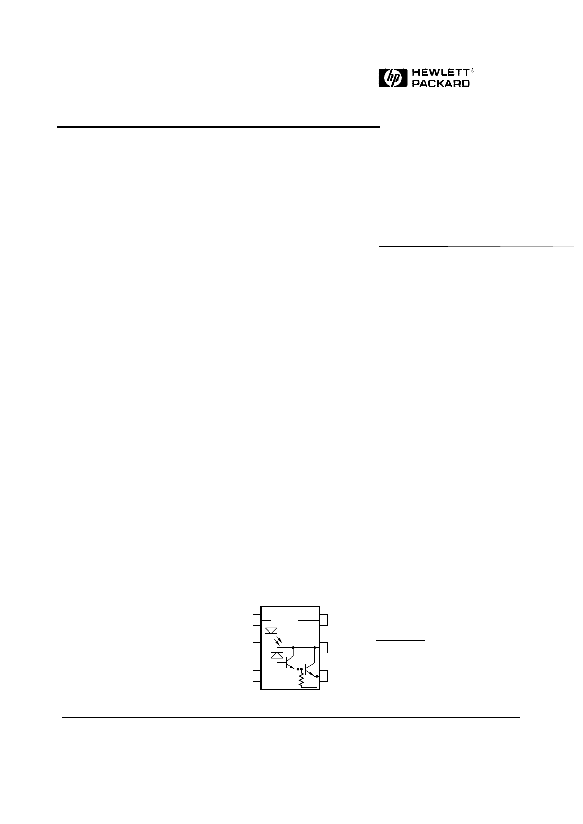
Functional Diagram
CAUTION: It is advised that normal static precautions be taken in handling and assembly of this component to
prevent damage and/or degradation which may be induced by ESD.
TRUTH TABLE
(POSITIVE LOGIC)
LED OUTPUT
ON L
OFF H
5
1
2
3
4
6
ANODE
CATHODE
V
B
GND
V
O
Description
The 4N45/46 optocouplers
contain a GaAsP light emitting
diode optically coupled to a high
gain photodetector IC.
The high current transfer ratio at
very low input currents permits
circuit designs in which adequate
margin can be allowed for the
effects of optical coupling
variations.
5965-3576E1-434
Page 2
Ordering Information
Specify part number followed by Option Number (if desired).
4N45#XXX
300 = Gull Wing Surface Mount Lead Option
500 = Tape/Reel Package Option (1 K min)
Option data sheets available. Contact your Hewlett-Packard sales representative or authorized distributor for
information.
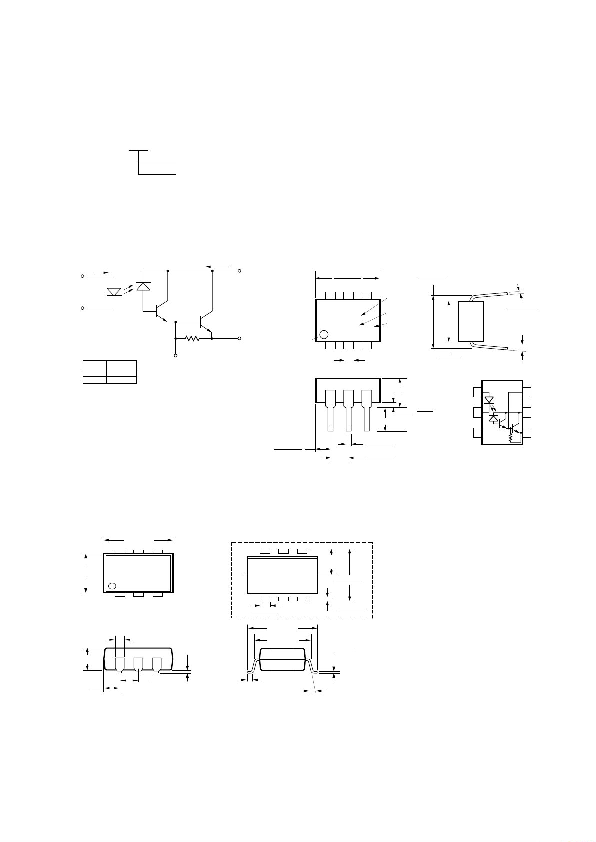
Outline Drawing
Outline Drawing – Option 300
9.40 (0.370)
9.90 (0.390)
PIN
ONE
DOT
HPXXXX
YYWW
TYPE
NUMBER
DATE CODE
2.16 (0.085)
2.54 (0.100)
2.28 (0.090)
2.80 (0.110)
(0.020)
(0.040)
0.45 (0.018)
0.65 (0.025)
4.70 (0.185) MAX.
2.66 (0.105) MIN.
6.10 (0.240)
6.60 (0.260)
0.20 (0.008)
0.33 (0.013)
5° TYP.
7.36 (0.290)
7.88 (0.310)
DIMENSIONS IN MILLIMETERS AND (INCHES).
1
2
3
56
321
CATHODE
ANODE
GND
V
V
B
O
1.78 (0.070) MAX.
R
U
4
UL
RECOGNITION
5
4
6
Schematic
I
F
1
2
V
F
ANODE
CATHODE
+
–
V
B
5
4
GND
V
O
I
O
6
TRUTH TABLE
(POSITIVE LOGIC)
LED
ON
OFF
OUTPUT
L
H
4N45 Outline – Option 300
4.19
(0.165)
2.29
(0.090)
2.54
(0.100)
TYP.
0.635 ± 0.130
(0.025 ± 0.005)
9.65 ± 0.25
(0.380 ± 0.010)
7.62 ± 0.25
(0.300 ± 0.010)
0.635 ± 0.25
(0.025 ± 0.010)
12° NOM.
0.20 (0.008)
0.30 (0.013)
1.78
(0.070)
MAX.
9.65 ± 0.25
(0.380 ± 0.010)
6.35 ± 0.25
(0.250 ± 0.010)
DIMENSIONS IN mm (INCHES)
TOLERANCES: xx.xx = 0.01
xx.xxx = 0.001
(unless otherwise specified)
LEAD COPLANARITY
MAXIMUM: 0.102 (0.004)
[3] [5]
1.194 (0.047)
1.778 (0.070)
4.826
(0.190)
TYP.
9.398 (0.370)
9.906 (0.390)
MAX.
PAD LOCATION (FOR REFERENCE ONLY)
0.381 (0.015)
0.635 (0.025)
1-435
Page 3
Regulatory Information
The 4N45 and 4N46 have been
approved by the following
regulatory organizations:
UL
Recognized under UL 1577,
Component Recognition
Program, File E55361.
CSA
Approved under CSA Component
Acceptance Notice #5, File CA
88324.
240
∆T = 115°C, 0.3°C/SEC
0
∆T = 100°C, 1.5°C/SEC
∆T = 145°C, 1°C/SEC
TIME – MINUTES
TEMPERATURE – °C
220
200
180
160
140
120
100
80
60
40
20
0
260
123456789101112
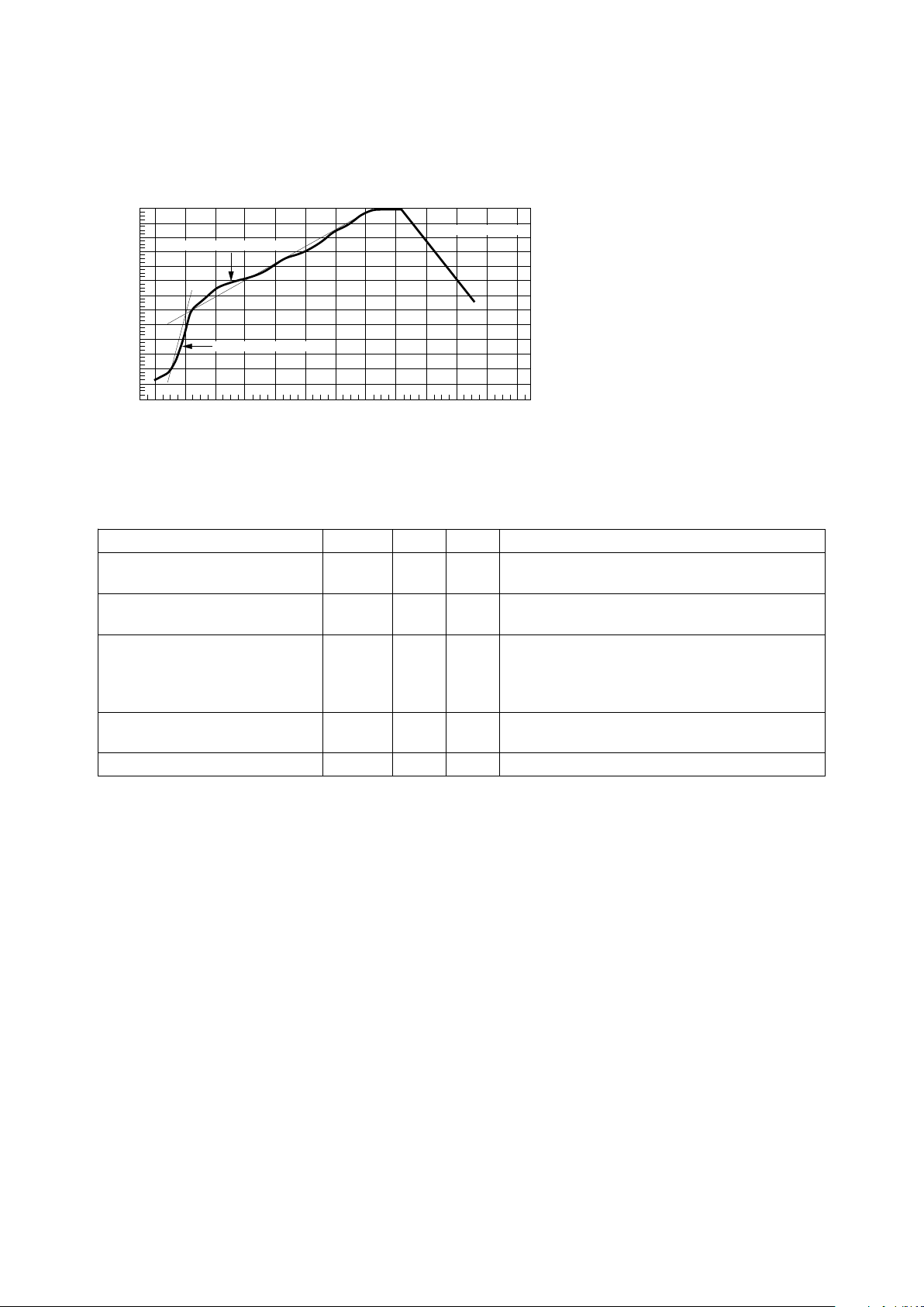
Thermal Profile (Option #300)
Figure 1. Maximum Solder Reflow Thermal Profile.
(Note: Use of non-chlorine activated fluxes is recommended.)
Insulation and Safety Related Specifications
Parameter Symbol Value Units Conditions
Min. External Air Gap L(IO1) 7.1 mm Measured from input terminals to output
(External Clearance) terminals, shortest distance through air
Min. External Tracking Path L(IO2) 7.4 mm Measured from input terminals to output
(External Creepage) terminals, shortest distance path along body
Min. Internal Plastic Gap 0.08 mm Through insulation distance, conductor to
(Internal Clearance) conductor, usually the direct distance
between the photoemitter and photodetector
inside the optocoupler cavity
Tracking Resistance CTI 200 Volts DIN IEC 112/VDE 0303 PART 1
(Comparative Tracking Index)
Isolation Group IIIa Material Group (DIN VDE 0110, 1/89, Table 1)
Option 300 – surface mount classification is Class A in accordance with CECC 00802.
Absolute Maximum Ratings
Storage Temperature, TS............................................. -55°C to +125°C
Operating Temperature, TA........................................... -40°C to +85°C
Lead Solder Temperature, max .......................................... 260°C for 10 s
(1.6 mm below seating plane)
Average Input Current, IF......................................................... 20 mA
[1]
Peak Input Current, IF................................................................... 40 mA
(50% duty cycle, 1 ms pulse width)
Peak Transient Input Current, IF...................................................... 1.0 A
(≤ 1 µs pulse width, 300 pps)
Reverse Input Voltage, VR.................................................................5 V
Input Power Dissipation, PI.................................................... 35 mW
[2]
Output Current, IO (Pin 5) ...................................................... 60 mA
[3]
Emitter-Base Reverse Voltage (Pins 4-6).......................................... 0.5 V
Output Voltage, VO (Pin 5-4)
4N45 ................................................................................. -0.5 to 7 V
4N46 ............................................................................... -0.5 to 20 V
Output Power Dissipation ..................................................... 100 mW
[4]
Infrared and Vapor Phase Reflow Temperature
(Option #300) .......................................... see Fig. 1, Thermal Profile
1-436
Page 4
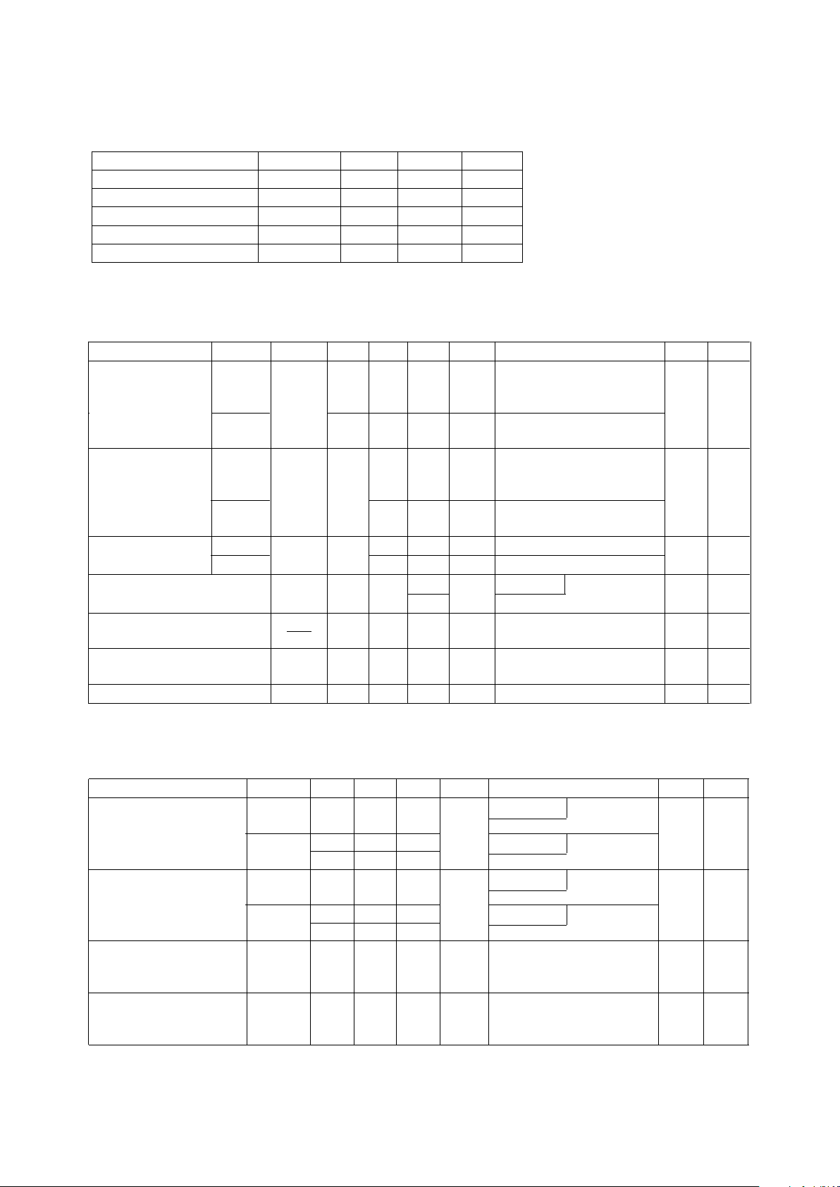
Switching Specifications
(Over recommended temperature TA = 0°C to 70°C unless otherwise specified. VCC = 5.0 V.
Parameter Symbol Min. Typ.* Max. Units Test Conditions Fig. Note
Propagation Delay Time t
PHL
80 µsT
A
= 25°CIF = 0.5 mA 6, 7, 6, 8
to Logic Low at Output RL = 10 kΩ 8, 9,
t
PHL
5 50* TA = 25°CIF = 10 mA
60 RL = 2.2 kΩ
Propagation Delay Time t
PLH
1500 µsT
A
= 25°CIF = 10 mA 6, 7, 6, 8
to Logic High at Output RL = 10 kΩ 8, 9,
t
PLH
150 500* TA = 25°CIF = 10 mA
600 RL = 220 kΩ
Common Mode |CMH| 500 V/µsIF = 0 mA, RL = 10 kΩ 10 9
Transient Immunity at |VCM| = 10 V
P-P
High Output Level
Common Mode |CML| 500 V/µsIF = 1.0 mA, RL = 10 kΩ 10 9
Transient Immunity at |VCM| = 10 V
P-P
Low Output Level
*JEDEC Registered Data.
**All typicals at TA = 25°C, unless otherwise noted.
DC Electrical Specifications
Over recommended temperature (TA = 0°C to 70°C), unless otherwise specified.
Parameter Device Symbol Min. Typ.* Max. Units Test Conditions Fig. Note
Current Transfer 4N46 CTR 350* 1500 3200 % IF = 0.5 mA, VO = 1.0 V 3, 4, 5, 6,
Ratio 500* 1500 2000 IF = 1.0 mA, VO = 1.0 V 5, 11, 8
200* 600 1000 IF = 10 mA, VO = 1.2 V 12
4N45 250* 1200 2000 % IF = 1.0 mA, VO = 1.0 V
200* 500 1000 IF = 10 mA, VO = 1.2 V
Logic Low 4N46 V
OL
0.90 1.0 V IF = 0.5 mA, IOL = 1.75 mA 3 6
Output Voltage 0.92 1.0 IF = 1.0 mA, IOL = 5.0 mA
0.95 1.2 IF = 10 mA, IOL = 20 mA
4N45 0.90 1.0 V IF = 1.0 mA, IOL = 2.5 mA
0.95 1.2 IF = 10 mA, IOL = 20 mA
Logic High 4N46 IOH* 0.001 100 µAIF = 0 mA, VO = 18 V 6
4N45 0.001 250 µAIF = 0 mA, VO = 5 V
Input Forward Voltage V
F
1.4 1.7* V TA = 25°CIF = 1.0 mA 2
1.75
Temperature Coefficient ∆V
F
-1.8 mV/°CIF = 1.0 mA
of Forward Voltage
Input Reverse Breakdown BVR*5 VIR = 10 µA
Voltage
Input Capacitance C
IN
60 pF f = 1 MHz, VF = 0
∆T
A
11, 13
11, 13
Output Current
Recommended Operating Conditions
Parameter Symbol Min. Max. Units
Output Voltage (4N46) V
O
4.5 20 V
Output Voltage (4N45) 4.5 7 V
Input Current (High) I
F(ON)
0.5 10 mA
Input Voltage (Low) V
F(OFF)
0 0.8 V
Operating Temperature T
A
070°C
1-437
Page 5
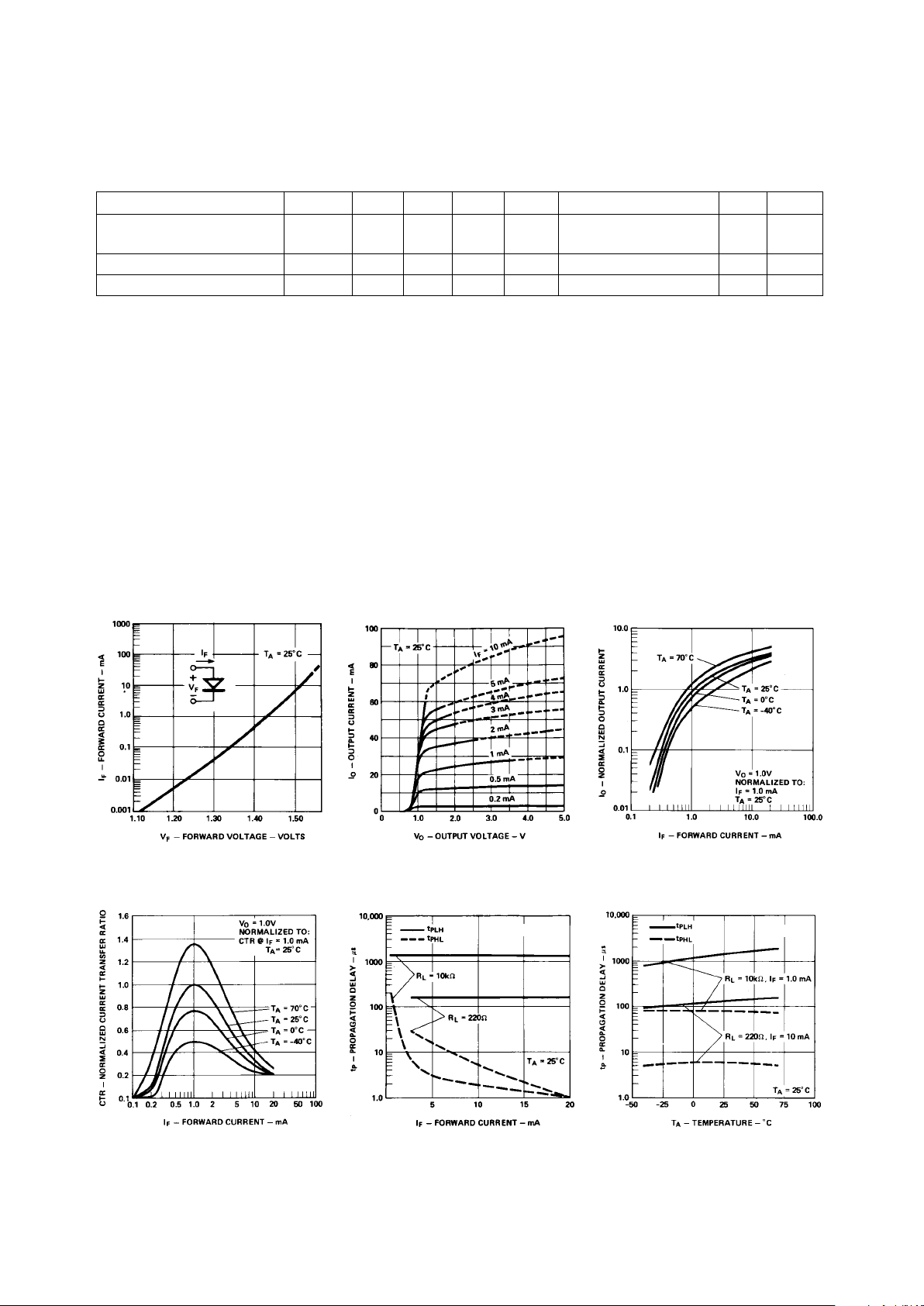
VCC = 5 V
VCC = 5 V
Figure 5. Current Transfer Ratio vs.
Input Current.
Figure 6. Propagation Delay vs.
Forward Current.
Figure 7. Propagation Delay vs.
Temperature.
Notes:
1. Derate linearly above 50°C free-air
temperature at a rate of 0.4 mA/°C.
2. Derate linearly above 50°C free-air
temperature at a rate of 0.7 mW/°C.
3. Derate linearly above 25°C free-air
temperature at a rate of 0.8 mA/°C.
4. Derate linearly above 25°C free-air
temperature at a rate of 1.5 mW/°C.
5. DC CURRENT TRANSFER RATIO is
defined as the ratio of output
collector current, IO, to the forward
LED input current, IF, times 100%.
6. Pin 6 Open.
Package Characteristics
For 0°C ≤ TA ≤ 70°C, unless otherwise specified. All typicals at TA = 25°C.
Parameter Symbol Min. Typ. Max. Units Test Conditions Fig. Notes
Input-Output Momentary V
ISO
2500 V rms RH ≤ 50%, t = 1 min, 7, 10
Withstand Voltage* TA = 25°C
Resistance, Input-Output R
I-O
10
12
Ω V
I-O
= 500 Vdc 7
Capacitance, Input-Output C
I-O
0.6 pF f = 1 MHz 7
*The Input-Output Momentary Withstand Voltage is a dielectric voltage rating that should not be interpreted as an input-output
continuous voltage rating. For the continuous voltage rating refer to the VDE 0884 Insulation Characteristics Table (if applicable),
your equipment level safety specification, or HP Application Note 1074, “Optocoupler Input-Output Endurance Voltage.”
maximum tolerable (negative)
dVcm/dt on the trailing edge of the
common mode pulse signal, Vcm, to
assure that the output will remain in
a Logic Low state (i.e., VO < 2.5 V).
10. In accordance with UL 1577, each
optocoupler is proof tested by
applying an insulation test voltage
≥ 3000 V rms for 1 second (leakage
detection current limit, I
I-O
≤ 5 µA).
7. Device considered a two-terminal
device: Pins 1, 2, 3 shorted together
and Pins 4, 5, and 6 shorted together.
8. Use of a resistor between pin 4 and 6
will decrease gain and delay time.
(See Figures 11, 12, and 13.)
9. Common mode transient immunity in
Logic High level is the maximum
tolerable (positive) dVcm/dt on the
leading edge of the common mode
pulse, VCM, to assure that the output
will remain in a Logic High state (i.e.,
VO > 2.5 V). Common mode transient
immunity in Logic Low level is the
Figure 2. Input Diode Forward
Current vs. Forward Voltage.
Figure 3. Typical DC Transfer
Characteristics.
Figure 4. Output Current vs. Input
Current.
1-438
Page 6
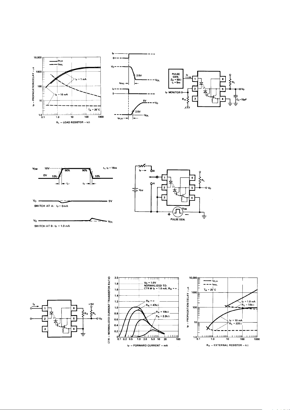
Figure 10. Test Circuit for Transient Immunity and Typical Waveforms.
+ 5 V (VCC)
Figure 8. Propagation Delay vs. Load
Resistor.
Figure 9. Switching Test Circuit.
VCC = 5 V
+ 5 V (VCC)
Figure 11. External Base Resistor, RX.
Figure 13. Effect of RX On
Propagation Delay.
Figure 12. Effect of RX On Current
Transfer Ratio.
VCC = 5 V
1-439
Page 7
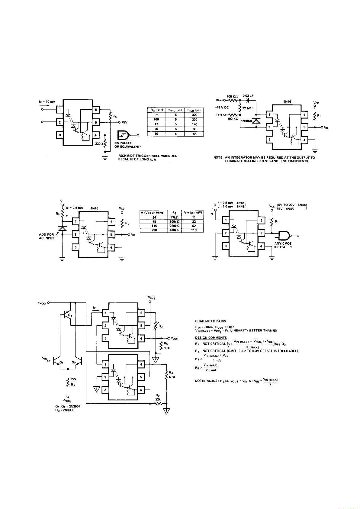
Analog Signal Isolation
Line Voltage Monitor CMOS Interface
TTL Interface Telephone Ring Detector
Applications
1-440
 Loading...