

Page 1
4N35, 4N36, 4N37
Vishay Semiconductors
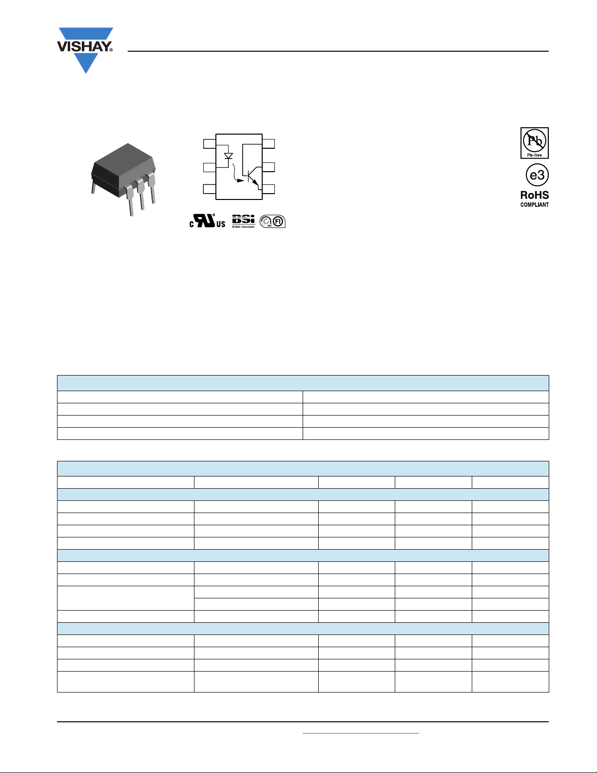
Optocoupler, Phototransistor Output, with Base Connection
FEATURES
1
A
C
2
3
NC
21842
i179004-5
DESCRIPTION
Each optocoupler consists of gallium arsenide infrared LED
and a silicon NPN phototransistor.
AGENCY APPROVALS
•
Underwriters laboratory file no. E52744
• BSI: EN 60065:2002, EN 60950:2000
•
FIMKO; EN 60065, EN 60335, EN 60950 certificate no. 25156
6
B
• Isolation test voltage 5000 V
RMS
• Interfaces with common logic families
5
C
4
E
• Input-output coupling capacitance < 0.5 pF
• Industry standard dual-in-line 6 pin package
• Compliant to RoHS directive 2002/95/EC and in
accordance to WEEE 2002/96/EC
APPLICATIONS
• AC mains detection
• Reed relay driving
• Switch mode power supply feedback
• Telephone ring detection
• Logic ground isolation
• Logic coupling with high frequency noise rejection
ORDER INFORMATION
PART REMARKS
4N35 CTR > 100 %, DIP-6
4N36 CTR > 100 %, DIP-6
4N37 CTR > 100 %, DIP-6
ABSOLUTE MAXIMUM RATINGS
PARAMETER TEST CONDITION SYMBOL VALUE UNIT
INPUT
Reverse voltage V
Forward current I
Surge current t ≤ 10 μs I
Power dissipation P
OUTPUT
Collector emitter breakdown voltage V
Emitter base breakdown voltage V
Collector current
Power dissipation P
COUPLER
Isolation test voltage V
Creepage ≥ 7mm
Clearance ≥ 7mm
Isolation thickness between emitter
and detector
(1)
t ≤ 1 ms I
F
FSM
diss
CEO
EBO
I
C
C
diss
ISO
R
6V
50 mA
1A
70 mW
70 V
7V
50 mA
100 mA
70 mW
5000 V
≥ 0.4 mm
RMS
www.vishay.com
Page 2
4N35, 4N36, 4N37
Vishay Semiconductors
Optocoupler, Phototransistor Output,
with Base Connection
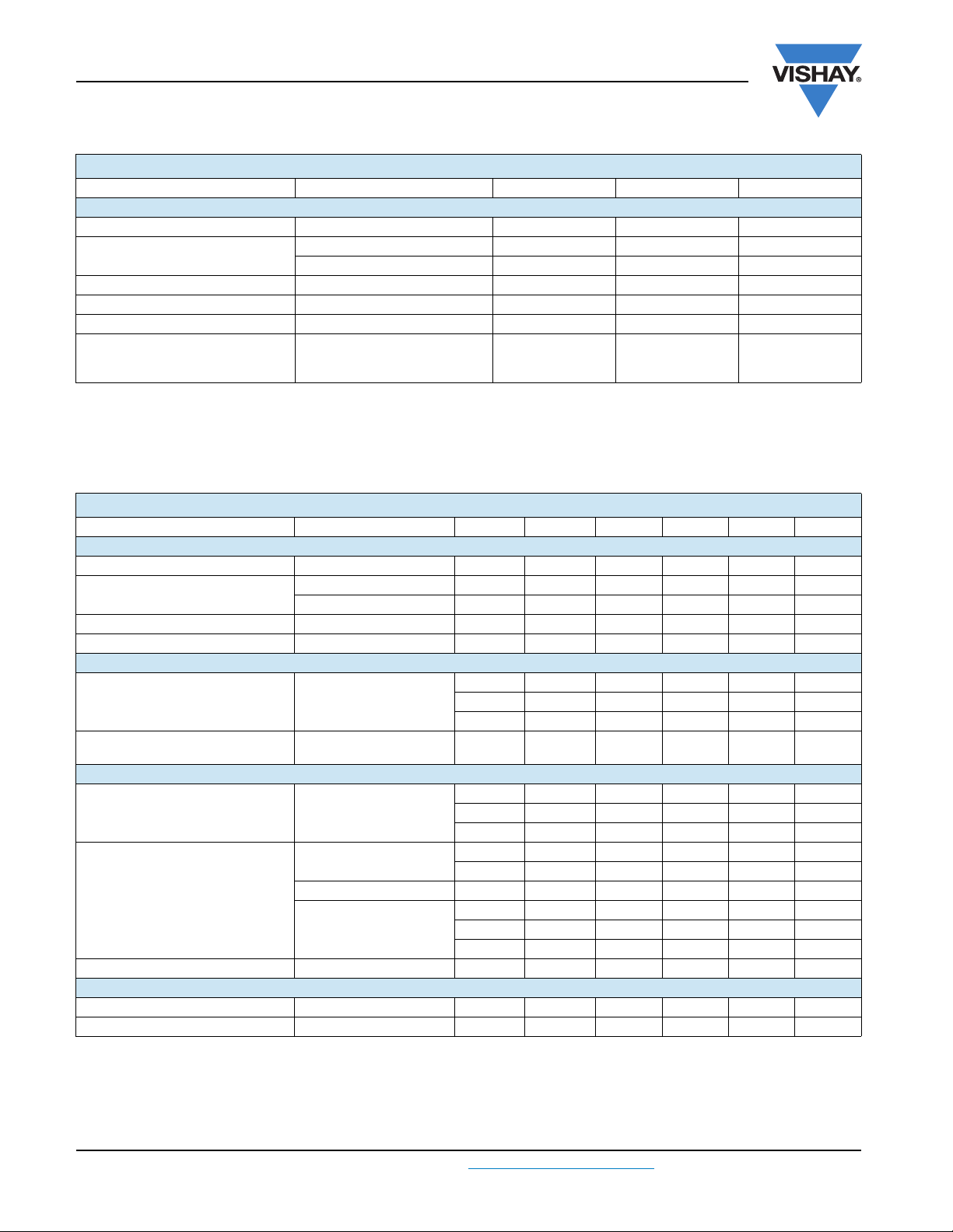
ABSOLUTE MAXIMUM RATINGS
PARAMETER TEST CONDITION SYMBOL VALUE UNIT
COUPLER
Comparative tracking index DIN IEC 112/VDE 0303, part 1 175
Isolation resistance
Storage temperature T
Operating temperature T
Junction temperature T
Soldering temperature
(2)
Notes
(1)
T
= 25 °C, unless otherwise specified.
amb
Stresses in excess of the absolute maximum ratings can cause permanent damage to the device. Functional operation of the device is not
implied at these or any other conditions in excess of those given in the operational sections of this document. Exposure to absolute
maximum ratings for extended periods of the time can adversely affect reliability.
(2)
Refer to wave profile for soldering condditions for through hole devices (DIP).
ELECTRICAL CHARACTERISTICS
PARAMETER TEST CONDITION PART SYMBOL MIN. TYP. MAX. UNIT
INPUT
Junction capacitance V
Forward voltage
Reverse current
Capacitance V
OUTPUT
Collector emitter breakdown
(2)
voltage
Emitter collector breakdown
(2)
voltage
OUTPUT
Collector base breakdown
(2)
voltage
Collector emitter leakage current
Collector emitter capacitance V
COUPLER
Resistance, input output
Capacitance, input output f = 1 MHz C
Notes
(1)
T
= 25 °C, unless otherwise specified.
amb
Minimum and maximum values are testing requirements. Typical values are characteristics of the device and are the result of engineering
evaluation. Typical values are for information only and are not part of the testing requirements.
(2)
Indicates JEDEC registered value.
(2)
I
(2)
(2)
(2)
(1)
V
= 500 V, T
IO
V
= 500 V, T
IO
= 25 °C R
amb
= 100 °C R
amb
max.10 s dip soldering:
distance to seating plane
≥ 1.5 mm
(1)
= 0 V, f = 1 MHz C
R
IF = 10 mA V
= 10 mA, T
F
= - 55 °C V
amb
VR = 6 V I
= 0 V, f = 1 MHz C
R
4N35 BV
IC = 1 mA
4N36 BV
4N37 BV
IE = 100 μA BV
4N35 BV
IC = 100 μA, IB = 1 μA
4N36 BV
4N37 BV
VCE = 10 V, IF = 0
V
= 10 V, IF = 0 4N37 I
CE
V
= 30 V, IF = 0,
CE
T
= 100 °C
amb
= 0 C
CE
4N35 I
4N36 I
4N35 I
4N36 I
4N37 I
VIO = 500 V R
T
IO
IO
stg
amb
sld
CEO
CEO
CEO
CEO
CEO
CEO
j
F
F
R
O
CEO
CEO
CEO
ECO
CBO
CBO
CBO
CE
IO
IO
12
10
10
11
Ω
Ω
- 55 to + 150 °C
- 55 to + 100 °C
100 °C
260 °C
j
50 pF
1.3 1.5 V
0.9 1.3 1.7 V
0.1 10 μA
25 pF
30 V
30 V
30 V
7V
70 V
70 V
70 V
550nA
550nA
550nA
500 μA
500 μA
500 μA
6pF
11
10
0.6 pF
Ω
www.vishay.com For technical questions, contact: [email protected]
Document Number: 81181
154 Rev. 1.2, 07-Jan-10
Page 3
4N35, 4N36, 4N37
Optocoupler, Phototransistor Output,
Vishay Semiconductors
with Base Connection
CURRENT TRANSFER RATIO
PARAMETER TEST CONDITION PART SYMBOL MIN TYP. MAX UNIT
100 %
100 %
100 %
40 50 %
40 50 %
40 50 %
off
10 μs
DC current transfer ratio
Note
(1)
Indicates JEDEC registered values.
(1)
VCE = 10 V, IF = 10 mA
V
= 10 V, IF = 10 mA,
CE
T
= - 55 °C to + 100 °C
A
4N35 CTR
4N36 CTR
4N37 CTR
4N35 CTR
4N36 CTR
4N37 CTR
DC
DC
DC
DC
DC
DC
SWITCHING CHARACTERISTICS
PARAMETER TEST CONDITION SYMBOL MIN. TYP. MAX. UNIT
Switching time
Note
(1)
Indicates JEDEC registered values.
(1)
VCC = 10 V, IC = 2 mA, RL = 100 Ω ton, t
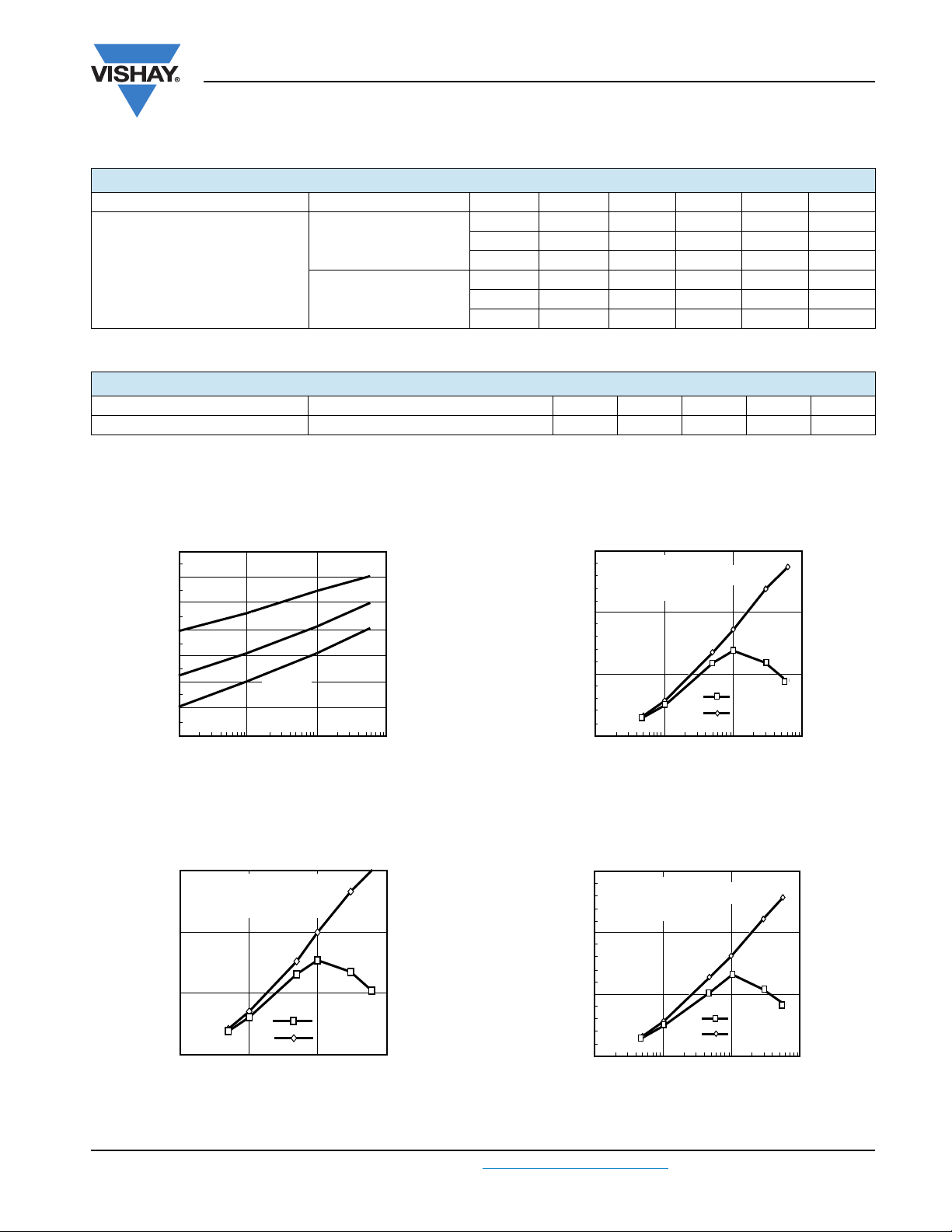
TYPICAL CHARACTERISTICS
T
= 25 °C, unless otherwise specied
amb
1.4
1.3
1.2
1.1
1.0
0.9
-Forward Voltage (V)
F
V
0.8
0.7
i4n25_01
TA = - 55 °C
TA = 25 °C
TA = 85 °C
IF - Forward Current (mA)
Fig. 1 - Forward Voltage vs. Forward Current
1001010.1
Fig. 3 - Normalized Non-Saturated and Saturated CTR vs.
1.5
Normalized to:
V
= 10 V, IF = 10 mA, TA = 25 °C
CE
CTR
CE(sat) VCE
1.0
T
= 50 °C
A
0.5
- Normalized CTR
CTR
N
0.0
i4n25_03
= 0.4 V
NCTR(SAT)
NCTR
1001010.1
IF - LED Current (mA)
LED Current
1.5
Normalized to:
= 10 V, IF = 10 mA, TA = 25 °C
V
CE
CTR
= 0.4 V
CE(sat)
1.0
T
= 25 °C
A
0.5
NCTR - Normalized CTR
0.0
0 10 100
i4n25_02
1
IF - LED Current (mA)
NCTR(SAT)
NCTR
Fig. 2 - Normalized Non-Saturated and Saturated CTR vs.
LED Current
Fig. 4 - Normalized Non-Saturated and Saturated CTR vs.
1.5
Normalized to:
= 10 V, IF = 10 mA, TA = 25 °C
V
1.0
0.5
CE
CTR
T
A
= 70 °C
CE(sat) VCE
= 0.4 V
NCTR - Normalized CTR
0.0
i4n25_04
IF - LED Current (mA)
LED Current
NCTR(SAT)
NCTR
1001010.1
Document Number: 81181 For technical questions, contact: [email protected]
www.vishay.com
Rev. 1.2, 07-Jan-10 155
Page 4
4N35, 4N36, 4N37
Vishay Semiconductors
1.5
Normalized to:
= 10 V, IF = 10 mA, TA = 25 °C
V
CE
CTR
CE(sat) VCE
= 0.4 V
Optocoupler, Phototransistor Output,
1.0
= 85 °C
T
A
0.5
NCTR - Normalized CTR
0.0
i4n25_05
IF - LED Current (mA)
NCTR(SAT)
NCTR
1001010.1
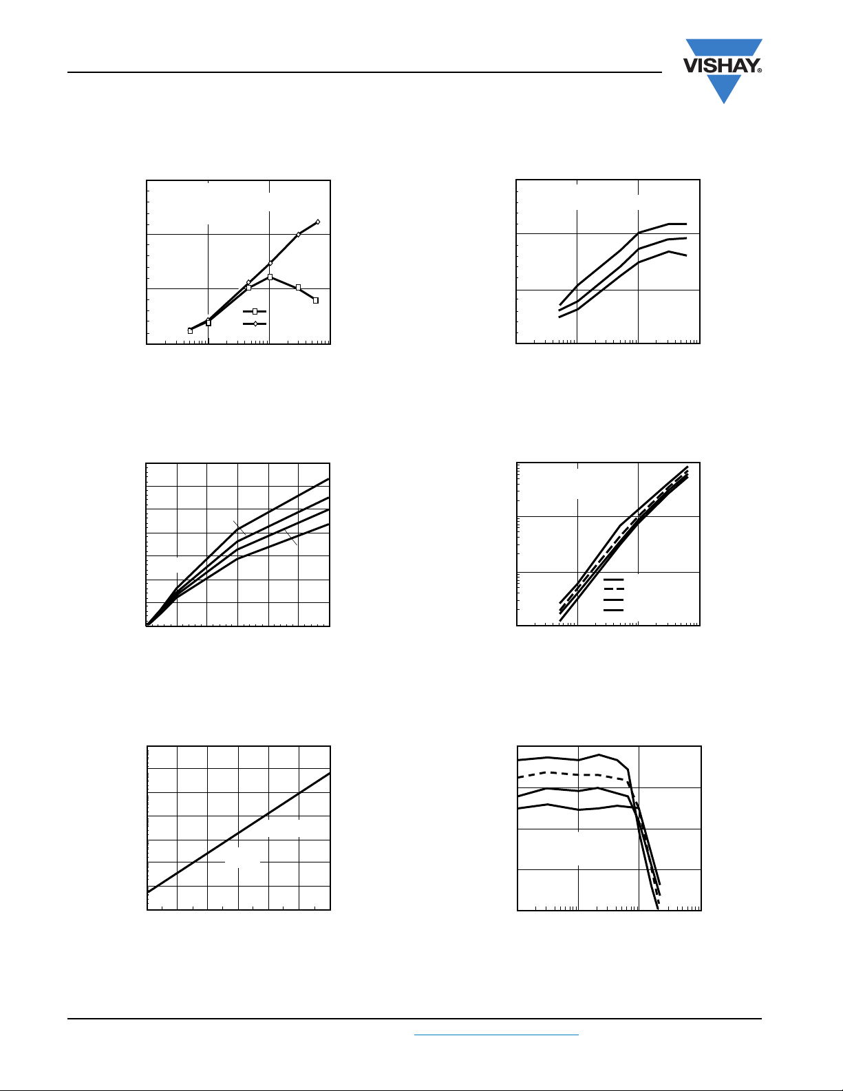
Fig. 5 - Normalized Non-Saturated and Saturated CTR vs.
LED Current
35
30
25
50 °C
20
15
25 °C
85 °C
70 °C
10
- Collector Current (mA)
5
CE
I
0
i4n25_06
IF - LED Current (mA)
Fig. 6 - Collector Emitter Current vs.
Temperature and LED Current
with Base Connection
Fig. 8 - Normalized CTRcb vs. LED Current and Temperature
6050403020100
Fig. 9 - Normalized Photocurrent vs. I
1.5
Normalized to:
cb
VCB = 9.3 V, IF = 10 mA, TA = 25 °C
1.0
0.5
- Normalized CTR
cb
25 °C
50 °C
NCTR
70 °C
0.0
0.1 1 10 100
i4n25_08
IF - LED Current (mA)
10
Normalized to:
IF = 10 mA, TA = 25 °C
1
1
0.
Normalized Photocurrent
Nib, TA = - 20 °C
Nib, T
Nib, T
Nib, T
0.01
0.1 1 10 100
i4n25_09
IF - LED Current (mA)
= 20 °C
A
= 50 °C
A
= 70 °C
A
and Temperature
F
5
10
4
10
3
10
2
10
1
10
0
10
- Collector Emitter (nA)
- 1
CEO
10
I
- 2
10
i4n25_07
T
- Ambient Temperature (°C)
amb
VCE = 10 V
Typical
100806040200- 20
Fig. 7 - Collector Emitter Leakage Current vs. Temperature
1.2
1.0
FE
70 °C
25 °C
- 20 °C
0.8
Normalized to:
IB = 20 µA, VCE = 10 V,
- Normalized h
A
0.6
FE
= 25 °C
T
Nh
0.4
1 10 100 1000
i4n25_10
Ib - Base Current (µA)
Fig. 10 - Normalized Non-Saturated h
Base Current and Temperature
vs.
FE
www.vishay.com For technical questions, contact: [email protected]
Document Number: 81181
156 Rev. 1.2, 07-Jan-10
Page 5
4N35, 4N36, 4N37
Optocoupler, Phototransistor Output,
with Base Connection
1.5
FE
50 °C
70 °C
1.0
25 °C
- 20 °C
0.5
= 0.4 V
V
- Normalized Saturated h
FE(sat)
Nh
CE
0.0
1 10 100 1000
i4n25_11
Ib - Base Current (µA)
Fig. 11 - Normalized hFE vs. Base Current and Temperature
1000
IF = 10 mA, TA = 25 °C
= 5.0 V, Vth = 1.5 V
V
CC
t
PHL
100
Normalized to:
VCE = 10 V, Ib = 20 µA
= 25 °C
T
A
2.5
2.0
Vishay Semiconductors
f = 10 kHz
DF = 50 %
IF = 10 mA
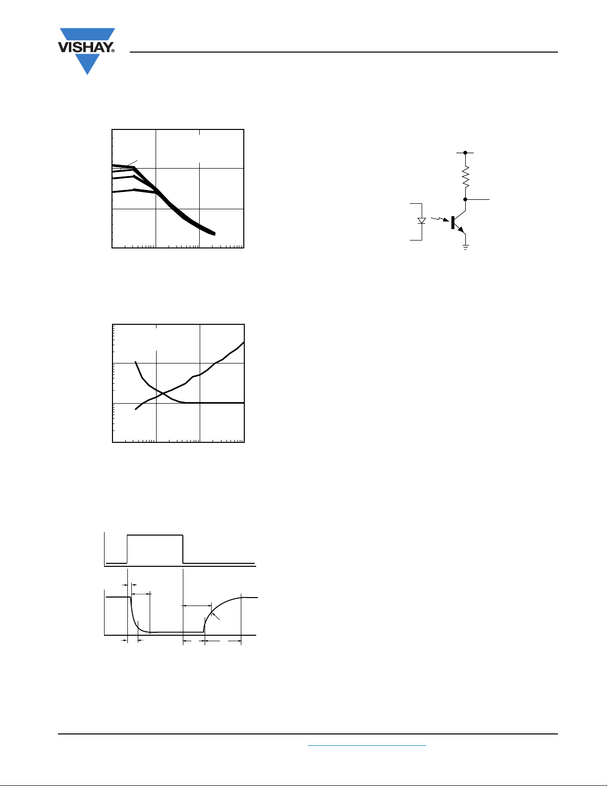
i4n25_14
Fig. 14 - Switching Schematic
VCC = 5 V
R
L
V
O
10
- Propagation Delay (µs)
PLH
t
i4n25_12
t
PLH
1
0.1 1 10 100
RL - Collector Load Resistor (kΩ)
1.5
1.0
Fig. 12 - Propagation Delay vs. Collector Load Resistor
I
F
t
D
t
PHL
t
R
t
PLH
= 1.5 V
V
TH
t
t
F
S
i4n25_13
V
O
Fig. 13 - Switching Timing
- Propagation Delay (µs)
PHL
t
Document Number: 81181 For technical questions, contact: [email protected]
www.vishay.com
Rev. 1.2, 07-Jan-10 157
Page 6
4N35, 4N36, 4N37
Vishay Semiconductors
Optocoupler, Phototransistor Output,
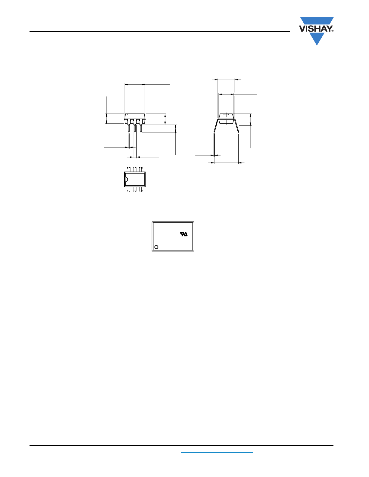
PACKAGE DIMENSIONS in millimeters
3.5 ± 0.3
0.5 ± 0.1
6 5 4
14771_2
1 2 3
with Base Connection
7.12 ± 0.3
4.5 ± 0.3
1.2 ± 0.1
2.8 ± 0.15
0.25
7.62 typ.
6.5 ± 0.3
4.5 ± 0.3
7.62 to 9.5 typ.
PACKAGE MARKING
4N35
V YWW 24
21764-24
Document Number: 81181
Page 7

Legal Disclaimer Notice
www.vishay.com
Vishay
Disclaimer
ALL PRODUCT, PRODUCT SPECIFICATIONS AND DATA ARE SUBJECT TO CHANGE WITHOUT NOTICE TO IMPROVE
RELIABILITY, FUNCTION OR DESIGN OR OTHERWISE.
Vishay Intertechnology, Inc., its affiliates, agents, and employees, and all persons acting on its or their behalf (collectively,
“Vishay”), disclaim any and all liability for any errors, inaccuracies or incompleteness contained in any datasheet or in any other
disclosure relating to any product.
Vishay makes no warranty, representation or guarantee regarding the suitability of the products for any particular purpose or
the continuing production of any product. To the maximum extent permitted by applicable law, Vishay disclaims (i) any and all
liability arising out of the application or use of any product, (ii) any and all liability, including without limitation special,
consequential or incidental damages, and (iii) any and all implied warranties, including warranties of fitness for particular
purpose, non-infringement and merchantability.
Statements regarding the suitability of products for certain types of applications are based on Vishay’s knowledge of typical
requirements that are often placed on Vishay products in generic applications. Such statements are not binding statements
about the suitability of products for a particular application. It is the customer’s responsibility to validate that a particular
product with the properties described in the product specification is suitable for use in a particular application. Parameters
provided in datasheets and/or specifications may vary in different applications and performance may vary over time. All
operating parameters, including typical parameters, must be validated for each customer application by the customer’s
technical experts. Product specifications do not expand or otherwise modify Vishay’s terms and conditions of purchase,
including but not limited to the warranty expressed therein.
Except as expressly indicated in writing, Vishay products are not designed for use in medical, life-saving, or life-sustaining
applications or for any other application in which the failure of the Vishay product could result in personal injury or death.
Customers using or selling Vishay products not expressly indicated for use in such applications do so at their own risk and agree
to fully indemnify and hold Vishay and its distributors harmless from and against any and all claims, liabilities, expenses and
damages arising or resulting in connection with such use or sale, including attorneys fees, even if such claim alleges that Vishay
or its distributor was negligent regarding the design or manufacture of the part. Please contact authorized Vishay personnel to
obtain written terms and conditions regarding products designed for such applications.
No license, express or implied, by estoppel or otherwise, to any intellectual property rights is granted by this document or by
any conduct of Vishay. Product names and markings noted herein may be trademarks of their respective owners.
Material Category Policy
Vishay Intertechnology, Inc. hereby certifies that all its products that are identified as RoHS-Compliant fulfill the
definitions and restrictions defined under Directive 2011/65/EU of The European Parliament and of the Council
of June 8, 2011 on the restriction of the use of certain hazardous substances in electrical and electronic equipment
(EEE) - recast, unless otherwise specified as non-compliant.
Please note that some Vishay documentation may still make reference to RoHS Directive 2002/95/EC. We confirm that
all the products identified as being compliant to Directive 2002/95/EC conform to Directive 2011/65/EU.
Revision: 12-Mar-12
1
Document Number: 91000
 Loading...