

Page 1
®
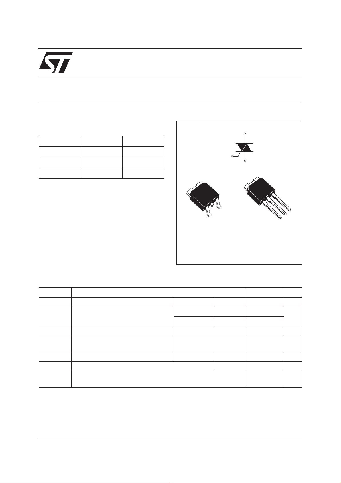
T405Q-600
Sensitive 4Q 4A TRIAC
MAIN FEATURES
A2
Symbol Value Unit
I
T(RMS)
V
DRM/VRRM
I
GT
4A
600 V
5mA
A2
G
A1
A2
DESCRIPTION
G
DPAK
A1
A2
A1
T405Q-600H
IPAK
The T405Q-600B-TR and the T405Q-600H 4
quadrants sensitive TRIACs are intended in general purpose applications where high surge current capability is required, such as irrigation
systems. These TRIACs feature a gate current capability sensitivities of 5mA.
T405Q-600B-TR
ABSOLUTE MAXIMUM RATINGS
Symbol Parameter Value Unit
I
T(RMS)
I
TSM
2
I
tI
dI/dt Critical rate of rise of on-state current
I
GM
P
G(AV)
T
stg
T
j
RMS on-state current (Full sine wave) DPAK / IPAK Tc= 110°C 4 A
Non repetitive surge peak on-state
current (Full cycle, T
2
t Value for fusing tp = 10 ms 6 A2s
initial = 25°C )
j
F = 50Hz t = 20ms 35 A
F = 60Hz t = 16.7ms 38
Repetitive F = 100 Hz 50 A/µs
=2xIGT,tr≤ 100ns
I
G
Peak gate current tp = 20µs Tj = 125°C 4 A
Average gate power dissipation Tj = 125°C 0.5 W
Storage junction temperature range
Operating junction temperature range
-40to+150
-40to+125
G
A2
°C
April 2004 - Ed: 1
1/7
Page 2
T405Q-600
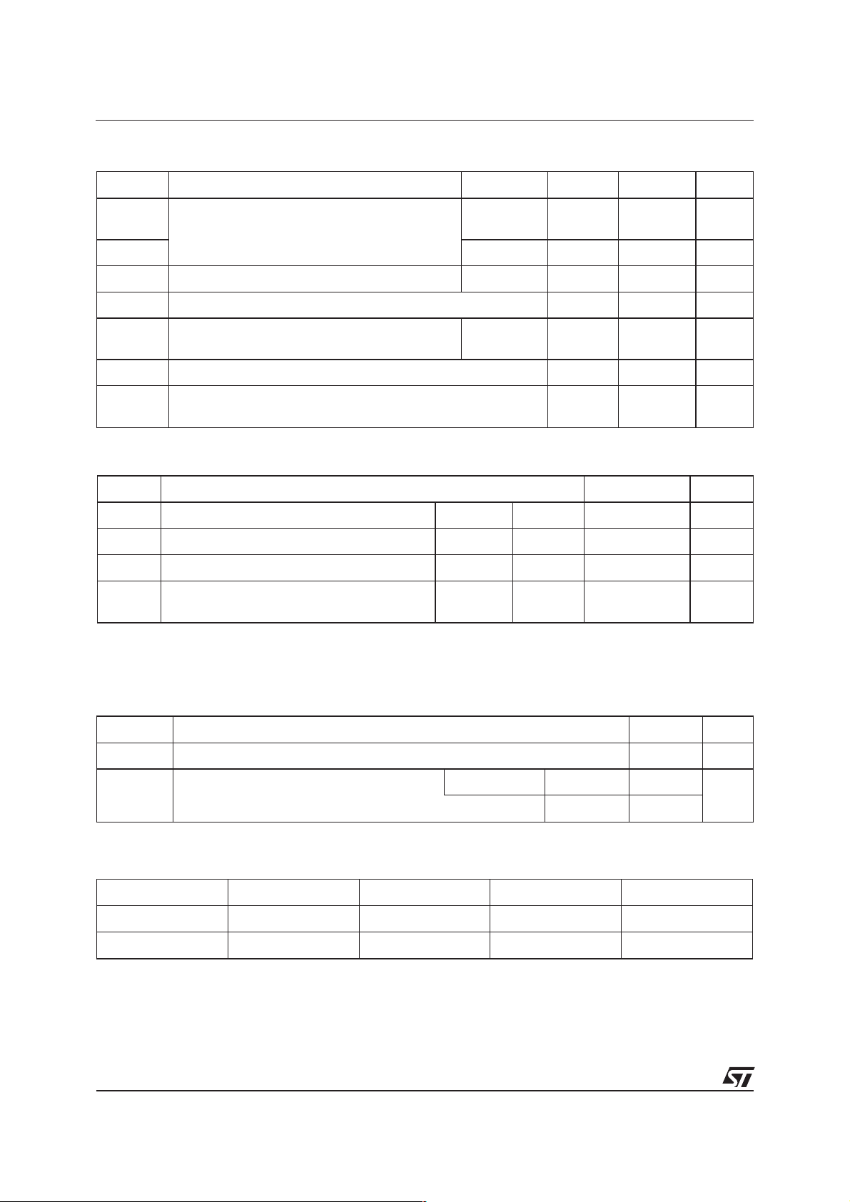
ELECTRICAL CHARACTERISTICS (Tj = 25°C, unless otherwise specified)
Symbol Test Conditions Quadrant T405Q Unit
(1)
I
GT
VD=12V RL=30Ω
I-II-III
IV
MAX. 5
10
mA
V
GT
V
GD
(2)
I
H
I
L
(2)
dV/dt
(dV/dt)c
(2)
VD=V
DRMRL
=3.3kΩ Tj = 125°C ALL MIN. 0.2 V
IT= 100mA MAX. 10 mA
IG= 1.2I
VD=67% V
GT
Gate open Tj = 125°C MIN. 10 V/µs
DRM
(dI/dt)c = 1.8 A/ms Tj = 125°C MIN. 2 V/µs
ALL MAX. 1.3 V
I-III-IV
II
MAX. 10
15
STATIC CHARACTERISTICS
Symbol Test Conditions Value Unit
(2)
V
TM
V
TO
R
d
I
DRM
I
RRM
Note 1: Minimum IGT is guaranted at 5% of IGT max.
Note 2: For both polarities of A2 referenced to A1.
ITM= 5 A tp = 380µs Tj = 25°C MAX. 1.5 V
(2)
Threshold voltage Tj = 125°C MAX. 0.85 V
(2)
Dynamic resistance Tj = 125°C MAX. 100 mΩ
V
DRM=VRRM
Tj = 25°C
Tj = 125°C
MAX 5
1
mA
mA
µA
THERMAL RESISTANCES
Symbol Parameter Value Unit
Rth(j-c) Junction to case (AC) 3 °C/W
Rth(j-a) Junction to ambient S = 0.5 cm² DPAK 70 °C/W
IPAK 100
PRODUCT SELECTOR
Part Number Voltage Sensitivity Type Package
T405Q-600B-TR 600V 5 mA Sensitive DPAK
T405Q-600H 600V 5 mA Sensitive IPAK
2/7
Page 3
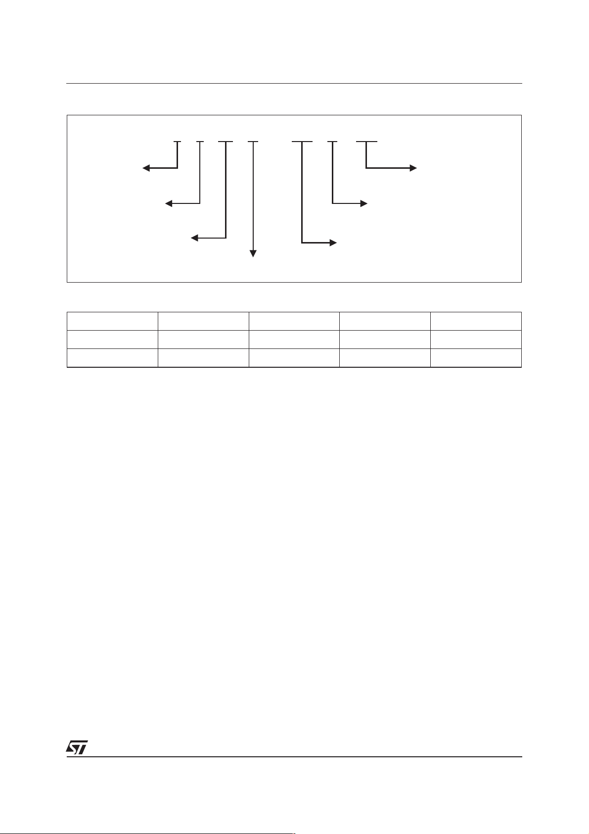
ORDERING INFORMATION
T 4 05 Q - 600 B (-TR)
T405Q-600
TRIAC SERIES
Current: 4A
Sensitivity:
5mA (Q1-Q2-Q3)
10mA (Q4)
Number of quadrants: 4
OTHER INFORMATION
Part Number Marking Weight Base quantity Packing mode
T405Q-600B-TR T405Q600 0.3 g 2500 Tape & reel
T405Q-600H T405Q600 0.4 g 75 Tube
Package:
B: DPAK
H: IPAK
Voltage: 600V
Packing mode:
Blank: Tube
-TR: DPAK Tape &reel
3/7
Page 4
T405Q-600
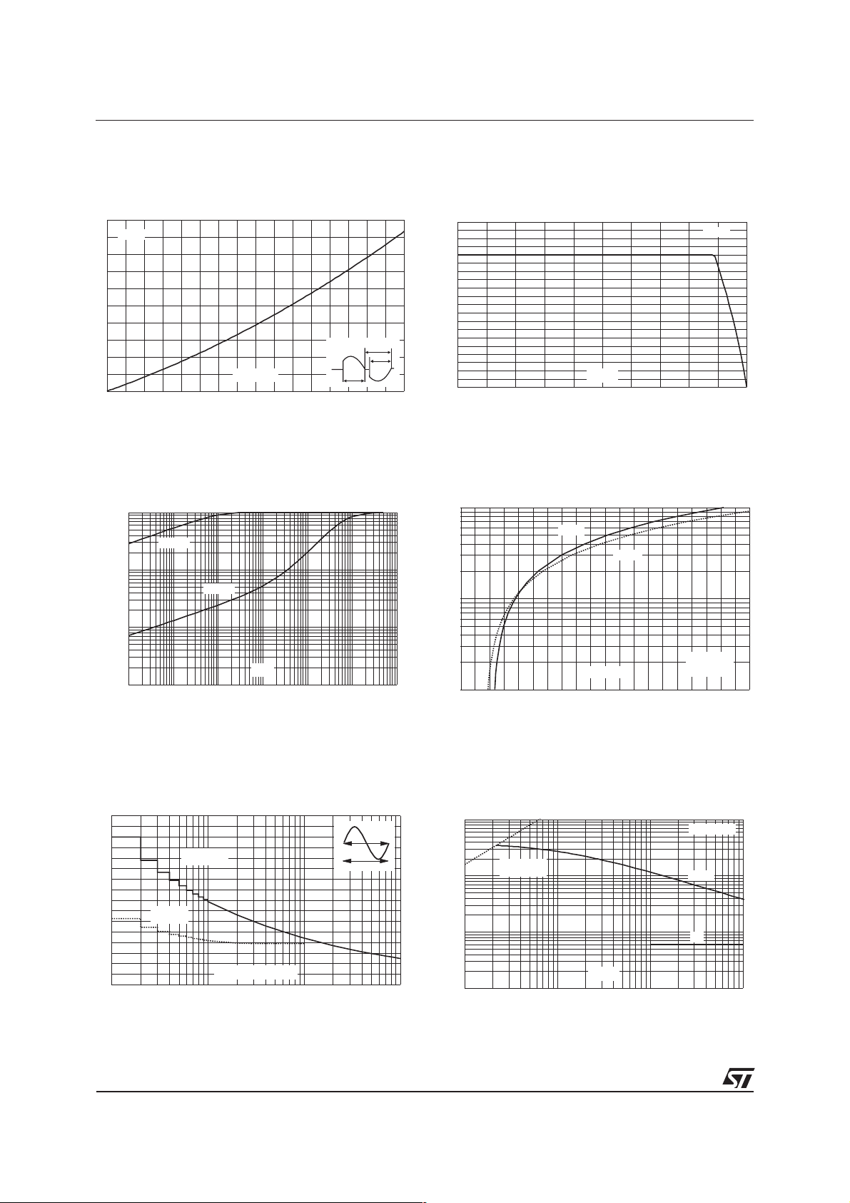
Fig. 1: Maximum power dissipation versus RMS
on-state current.
P(W)
5
α=180°
4
3
2
180°
1
I(A)T(RMS)
0
0.0 0.5 1.0 1.5 2.0 2.5 3.0 3.5 4.0
α
α
Fig. 3: Relative variation of thermal impedance
versus pulse duration.
K=[Zth/Rth]
1.E+00
Z
th(j-c)
1.E-01
Z
th(j-c)
Fig. 2: RMS on-state current versus case tem
perature.
I(A)T(RMS)
5.0
4.5
4.0
3.5
3.0
2.5
2.0
1.5
1.0
0.5
0.0
0 25 50 75 100 125
Tc(°C)
α=180°
Fig. 4: On-state characteristics (maximum val
ues).
I(A)TM
100
Tj=25°C
Tj=125°C
10
-
-
1.E-02
t (s)P
1.E-03
1.E-03 1.E-02 1.E-01 1.E+00 1.E+01 1.E+02 1.E+03
Fig. 5: Surge peak on-state current versus number
of cycles.
I(A)TSM
40
35
Repetitive
=110°C
T
C
Non repetitive
initial=25°C
T
j
Number of cycles
30
25
20
15
10
5
0
1 10 100 1000
t=20ms
One cycle
Tjmax. :
V
= 0.85 V
to
= 100 mΩ
R
V(V)TM
1
012345678 910
d
Fig. 6: Non repetitive surge peak on-state current
for a sinusoidal pulse with width tp<10ms, and
corresponding value of I
I (A), I²t(A²s)TSM
1000
dI/dt limitation:
100
10
1
0.01 0.10 1.00 10.00
50A/µs
2
t.
tp(ms)
Tjinitial=25°C
I
TSM
I²t
4/7
Page 5
T405Q-600
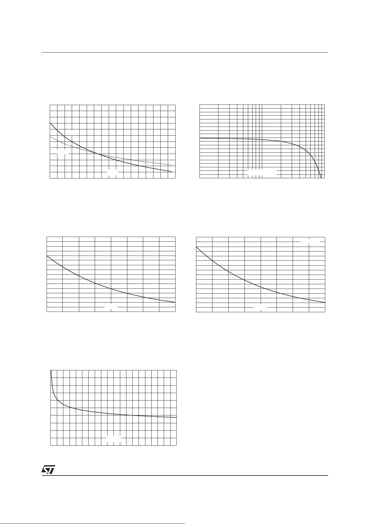
Fig. 7: Relative variation of gate trigger current,
holding current and latching current versus junc
tion temperature (typical values).
I , I , I [Tj] / I , I , I [Tj = 25°C]
GT H L GT H L
3.0
2.5
2.0
1.5
1.0
0.5
0.0
-40 -30 -20 -10 0 10 20 30 40 50 60 70 80 90 100 110 120 130
IH& I
I
GT
L
Tj(°C)
Fig. 9: Relative variation of critical rate of decrease
of main current versus junction temperature.
(dI/dt)c [Tj] / (dI/dt)c [Tj = 125°C]
8
7
6
5
4
3
2
1
0
25 50 75 100 125
Tj(°C)
Fig. 8: Relative variation of critical rate of decrease
of main current versus reapplied dV/dt (typical val
ues).
(dI/dt)c [(dV/dt)c] / Specified (dI/dt)c
2.0
1.8
1.6
1.4
1.2
1.0
0.8
0.6
0.4
0.2
0.0
0.1 1.0 10.0
(dV/dt)c (V/µs)
Fig. 10: Relative variation of static dV/dt immunity
versus junction temperature.
dV/dt [Tj] / dV/dt [Tj = 125°C]
8
7
6
5
4
3
2
1
0
25 50 75 100 125
Tj(°C)
-
VD=VR=400V
Fig. 11: Thermal resistance junction to ambient
versus copper surface under tab (epoxy printed
circuit board FR4, Cu = 35µm).
Rth(j-a)(°C/W)
100
90
80
70
60
50
40
30
20
10
0
02468101214161820
S(cm²)
5/7
Page 6
T405Q-600
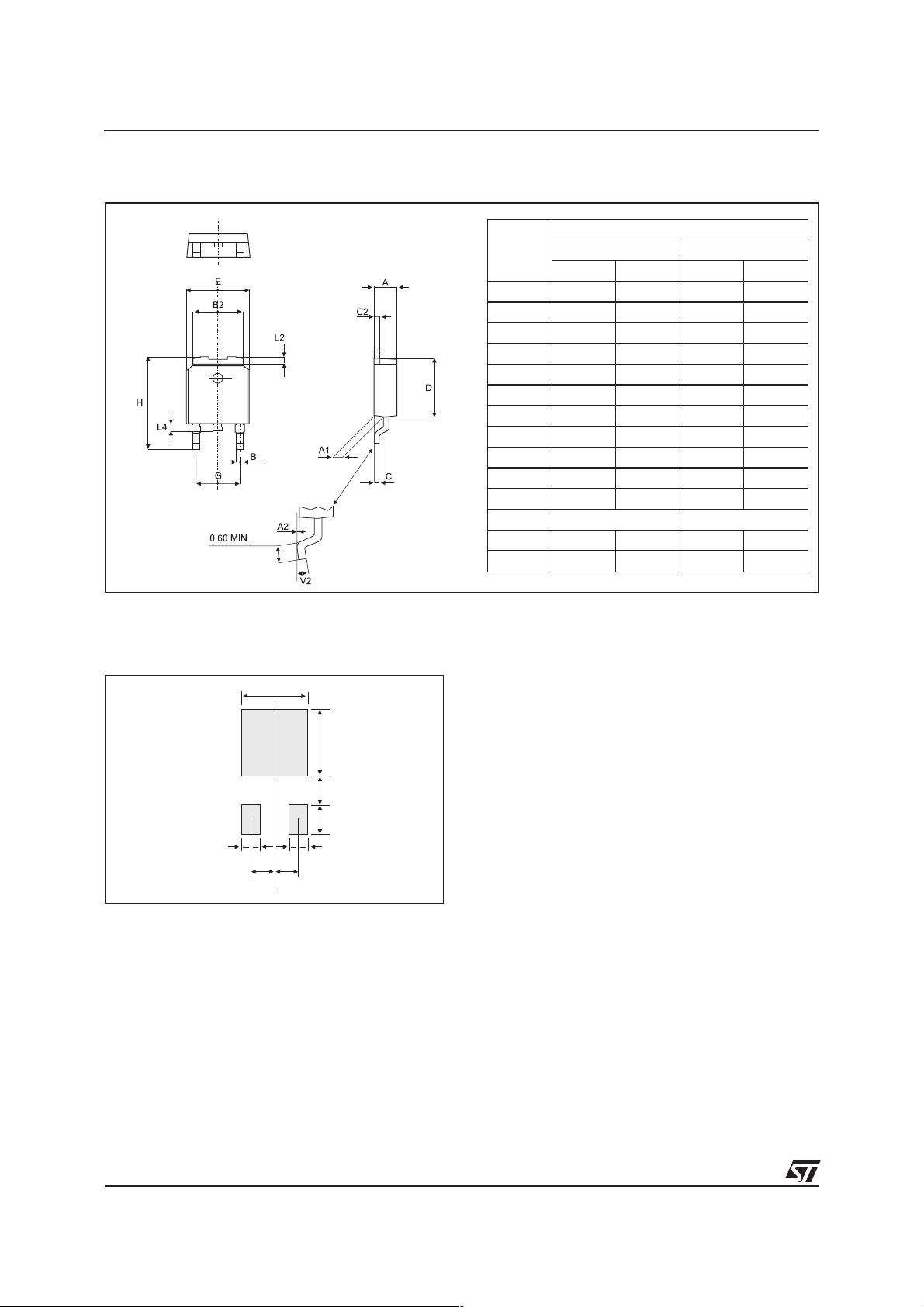
PACKAGE MECHANICAL DATA
DPAK
DIMENSIONS
REF.
Millimeters Inches
Min. Max Min. Max.
A 2.20 2.40 0.086 0.094
A1 0.90 1.10 0.035 0.043
A2 0.03 0.23 0.001 0.009
B 0.64 0.90 0.025 0.035
B2 5.20 5.40 0.204 0.212
C 0.45 0.60 0.017 0.023
C2 0.48 0.60 0.018 0.023
D 6.00 6.20 0.236 0.244
E 6.40 6.60 0.251 0.259
G 4.40 4.60 0.173 0.181
H 9.35 10.10 0.368 0.397
L2 0.80 typ. 0.031 typ.
L4 0.60 1.00 0.023 0.039
V2 0° 8° 0° 8°
FOOTPRINT
6.7
6.7
3
3
1.61.6
2.32.3
6/7
Page 7
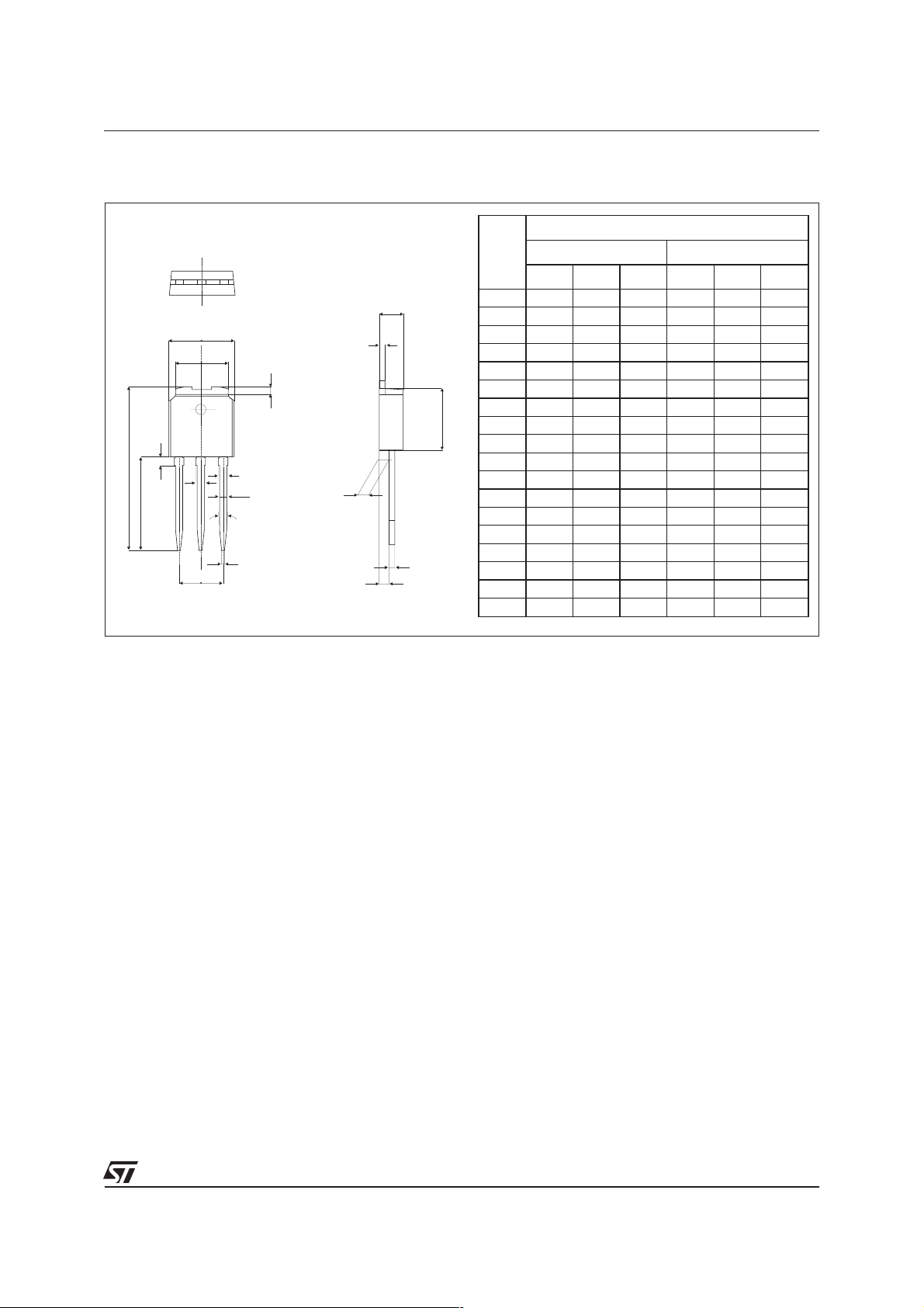
PACKAGE MECHANICAL DATA
IPAK
E
B2
H
L1
L
B6
G
L2
B3
B
V1
B5
T405Q-600
DIMENSIONS
REF.
A
C2
A 2.2 2.4 0.086 0.094
A1 0.9 1.1 0.035 0.043
A3 0.7 1.3 0.027 0.051
B 0.64 0.9 0.025 0.035
B2 5.2 5.4 0.204 0.212
B3 0.85 0.033
D
B5 0.3 0.035
B6 0.95 0.037
C 0.45 0.6 0.017 0.023
C2 0.48 0.6 0.019 0.023
A1
D 6 6.2 0.236 0.244
E 6.4 6.6 0.252 0.260
G 4.4 4.6 0.173 0.181
H 15.9 16.3 0.626 0.641
C
A3
L 9 9.4 0.354 0.370
L1 0.8 1.2 0.031 0.047
L2 0.8 1 0.031 0.039
V1 10° 10°
Millimeters Inches
Min. Typ. Max. Min. Typ. Max.
Information furnished is believed to be accurate and reliable. However, STMicroelectronics assumes no responsibility for the consequences of
use of such information nor for any infringement of patents orother rights of third parties which may result from its use. No license is granted by
implication or otherwise under any patent or patent rights of STMicroelectronics. Specifications mentioned in this publication are subject to
change without notice. This publication supersedes and replaces all information previously supplied. STMicroelectronics products are not au
thorized for use as critical components in life support devices or systems without express written approval of STMicroelectronics.
The ST logo is a registered trademark of STMicroelectronics.
All other names are the property of their respective owners.
© 2004 STMicroelectronics - All rights reserved.
STMicroelectronics GROUP OF COMPANIES
Australia - Belgium - Brazil - Canada - China - Czech Republic - Finland - France - Germany -
Hong Kong - India - Israel - Italy - Japan - Malaysia - Malta - Morocco - Singapore - Spain -
Sweden - Switzerland - United Kingdom - United States
www.st.com
7/7
-
 Loading...