


Preliminary Data Sheet
September 2000
3X38FTR 208-Pin SQFP
OCTAL-FET (Fast Ethernet Transceiver) for 10Base-T/100Base-TX/
■
Overview
The 3X38FTR 208-Pin SQFP is an eight-channel,
single-chip complete transceiver designed specifically for dual-speed 10Base-T, 100Base-TX, and
100Base-FX switches and repeaters. It supports
simultaneous operation in three separate
IEEE
*
standard modes: 10Base-T, 100Base-TX, and
100Base-FX. The 3X38 uses 0.25 µm low-power
CMOS to achieve extremely low power dissipation
and operates from a single 3.3 V power supply.
Each channel implements the following:
■
10Base-T transceiver function of
■
100Base-TX transceiver function of
■
100Base-FX transceiver function of
■
Autonegotiation of
■
MII management of
IEEE
IEEE
802.3u.
802.3u.
IEEE
IEEE
IEEE
802.3.
802.3u.
802.3u.
The 3X38 supports operations over two pairs of
unshielded twisted-pair (UTP) cable (10Base-T and
100Base-TX) and over fiber-optic cable (100BaseFX).
It has been designed with a flexible system interface
that allows configuration for optimum performance
and effortless design. The individual per-port system
interface can be configured as 10 Mbits/s,
or
100 Mbits/s reduced MII (RMII), or 10 Mbits/s, or
100 Mbits/s serial MII (SMII).
Features
10 Mbits/s Transceiver
■
Compatible with
for category 3 unshielded twisted-pair (UTP) cable.
■
Compatible with the reduced MII (RMII) specifica-
tion of the RMII consortium version 1.2.
■
Selectable 7-pin RMII or 2-pin serial MII (SMII).
IEEE
802.3 10Base-T standard
Autopolarity detection and correction.
■
Adjustable squelch level for extended line length
capability (two levels).
■
On-chip filtering eliminates the need for external
filters.
■
Half- and full-duplex operations.
100 Mbits/s TX Transceiver
■
Compatible with
IEEE
802.3u PCS (clause 23),
PMA (clause 24), autonegotiation (clause 28), and
PMD (clause 25) specifications.
■
Compatible with the reduced MII (RMII) specifica-
tion of the RMII consortium version 1.2.
■
Selectable 7-pin RMII, 2-pin SMII (serial MII).
■
Scrambler/descrambler bypass.
■
Selectable carrier sense signal generation (CRS)
asserted during eit her tr ansm issi on o r re cepti on i n
half duplex (CRS asserted during reception only in
full duplex).
■
Full- or half-duplex operations.
■
On-chip filtering and adaptive equalization that
eliminates the need for external filters.
100 Mbits/s FX Transceiver
■
Pseudo-ECL compatible input/output for 100Base-
FX support (with fiber-optic signal detect).
■
Compatible with
dard.
■
Reuses existing twisted-pair I/O pins for compati-
ble fiber-optic transceiver pseudo-ECL (PECL)
data:
— No additional data pins required.
— Reuses existing 3X38 pins for fiber-optic
signal detect (FOSD) inputs.
IEEE
802.3u 100Base-FX stan-
FX
*
IEEE
is a registered trademark of The Institute of Electrical and Electronics Engineers, Inc.

3X38FTR 208-Pin SQFP Preliminary Data Sheet
OCTAL-FET for 10Base-T/100Base-TX/FX September 2000
■
Features
■
Fiber mode automatically configures port:
(continued)
— Disables autonegotiation.
— Disables 10Base-T.
— Enables 100Base-FX far-end fault signaling.
— Disables MLT-3 encoder/decoder.
— Disables scrambler/descrambler.
■
FX mode enable is pin- or register-selectable on an
individual per-port basis.
General
■
Low power dissipation (<0.4 W per port).
■
Autonegotiation (
— Fast link pulse (FLP) burst generator.
— Arbitration function.
■
Supports the station management protocol and
frame format (clause 22):
— Basic and extended registers.
— Supports next page mode.
— Accepts preamble suppression.
— Maskable status interrupts.
— 12.5 MHz MDC clock rate.
■
Supports the following management functions via
pins if MII station management is unavailable:
— Speed select.
— Scrambler/descrambler bypass.
— Full duplex.
— No link pulse mode.
— Carrier sense select.
— Autonegotiation.
— FX mode select.
IEEE
802.3u, cl ause 28):
Single 50 MHz/125 MHz clock input in RMII and SMII
modes, respectively.
■
Supports half- and full-duplex operations.
■
Provides four LED status signals:
— Activity (transmit or receive). Optional LED blink
mode (500 ms on, 500 ms off or 2.5 s on, 2.5 s
off) or pulse stretch mode (40 ms—80 ms).
— Full duplex or collision, automatically configured.
— Link integrity.
— Speed indication.
■
Internally generated power-on-reset configures 3X38
automatically on powerup.
■
Serial LED output stream for additional status moni-
toring.
■
Bicolor LED mode.
■
LED drivers on-chip (8 mA—10 mA). Drivers can be
turned off when LED is not used (power saving).
■
Per-channel powerdown mode for 10 Mbits/s and
100 Mbits/s operation.
■
Loopback for 10 Mbits/s and 100 Mbits/s operation.
■
Internal pull-up or pull-down resistors to set default
configuration during powerup.
■
0.25 µm low-power CMOS technology.
■
208-pin SQFP package.
■
JTAG boundary scan.
■
Single 3.3 V power supply.
2 Lucent Technologies Inc.

Preliminary Data Sheet 3X38FTR 208-Pin SQFP
September 2000 OCTAL-FET for 10Base-T/100Base-TX/FX
Table of Contents
Contents Page
Overview...................................................................................................................................................................................................1
Features....................................................................................................................................................................................................1
10 Mbits/s Transceiver........................................................................................................................................................................... 1
100 Mbits/s TX Transceiver....................................................................................................................................................................1
100 Mbits/s FX Transceiver....................................................................................................................................................................1
General .................................................................................................................................................................................................. 2
Description................................................................................................................................................................................................5
RMII Mode............................................................................................................................................................................................. 5
SMII Mode.............................................................................................................................................................................................5
LED Control...........................................................................................................................................................................................5
Clocking................................................................................................................................................................................................. 5
FX Mode................................................................................................................................................................................................ 5
Single-Channel Detail Functions...........................................................................................................................................................7
Block Diagrams......................................................................................................................................................................................8
Pin Information ....................................................................................................................................................................................... 10
Pin Diagram for RMII Mode................................................................................................................................................................. 10
Pin Diagram for SMII Mode .................................................................................................................................................................11
Pin Maps........................... ....................................................................................................................... ............................................15
Pin Descriptions......................................................................................................................................................................................16
Functional Description............................................................................................................................................................................27
Reduced Media Independent Interface (RMII)..................................................................................................................................... 27
RMII/SMII Interface.............................................................................................................................................................................. 29
Media Independent Interface (MII)—Internal ....................................................................................................................................... 31
100Base-X Module.............................. ........................................................................................................................ ........................32
100Base-TX Transceiver......................................................................................................................................................................36
10Base-T Module................................................................................................................................................................................37
Operation Modes.................................................................................................................................................................................37
LED Operational Modes......................................................................................................................................................................39
Reset Operation...................................................................................................................................................................................43
MII Station Management ........................................................................................................................................................................44
Basic Operation...................................................................................................................................................................................44
Unmanaged Operations....................................................................................................................................................................... 45
Register Information............... ................................................................................................................................................................ 46
Register Descriptions ..........................................................................................................................................................................46
Absolute Maximum Ratings................................. ...................................................................................................................................56
Clock Timing............................................................................................... .................... ........................................................................57
Outline Diagram......................................................................................................................................................................................63
208-Pin SQFP .....................................................................................................................................................................................63
Tables Page
Table 1. 3X38 Signal in Alphanumer ic Sequenc e Ac cording to Pin Number.........................................................................................1 2
Table 2. 3X38 RMII/SMII Pin Map..........................................................................................................................................................15
Table 3. RMII/SMII Interface Pins..........................................................................................................................................................16
Table 4. MII Management......................................................................................................................................................................17
Table 5. 10/100 Mbits/s Twisted-Pair (TP) Interface Pins....................................................................................................................... 18
Table 6. LED and Configuration Pins.....................................................................................................................................................18
Table 7. Table Test Mode Pins...............................................................................................................................................................24
Table 8. Clock, Reset, FOSD, and Special Configuration Pins..............................................................................................................25
Table 9. Power, Ground, and No Connects ............................................................................................................................................26
Table 10. Receive Data/Status Encoding...............................................................................................................................................30
Table 11. Symbol Code Scrambler .......................................................................................................................................................33
Table 12. LED Modes ............................................................................................................................................................................40
Table 13. Serial LED Pin Descriptions...................................................................................................................................................41
Table 14. Serial LED Port Order............................................................................................................................................................41
Table 15. Bicolor Mode..........................................................................................................................................................................4 2
Table 16. Bicolor LED Mode Descriptions .............................................................................................................................................43
Table 17. MII Management Frame Format.................... ................................................................................ ......................................... 44
Table 18. MII Management Frames—Field Descriptions................. .................................................................................................... ..44
Lucent Technologies Inc. 3

3X38FTR 208-Pin SQFP Preliminary Data Sheet
OCTAL-FET for 10Base-T/100Base-TX/FX September 2000
Table of Contents
Tables
Table 19. PHY Addresses ......................................................................................................................................................................45
Table 20. Output Pins.............................................................................................................................................................................45
Table 21. Summary of Management Registers (MR).............................................................................................................................46
Table 22. MR0—Control Register Bit Descriptions.................................................................................................................................46
Table 23. MR1—Status Register Bit Descriptions..................................................................................................................................47
Table 24. MR2, MR3—PHY Identification Registers (1 and 2) Bit Descriptions.....................................................................................48
Table 25. MR4—Autonegotiation Advertisement Register Bit Descriptions...........................................................................................48
Table 26. MR5—Autonegotiation Link Partner Ability (Base Page) Register Bit Descriptions................................................................49
Table 27. MR5—Autonegotiation Link Partner (LP) Ability Register (Next Page) Bit Descriptions.........................................................49
Table 28. MR6—Autonegotiation Expansion Register Bit Descriptions..................................................................................................50
Table 29. MR7—Next Page Transmit Register Bit Descriptions .............................................................................................................50
Table 30. MR20—LED and FIFO Configuration.....................................................................................................................................51
Table 31. MR21—RXER Counter...........................................................................................................................................................51
Table 32. MR28—Device-Specific Register 1 (Status Register) Bit Descriptions...................................................................................52
Table 33. MR29—Device-Specific Register 2 (100 Mbits/s Control) Bit Descriptions............................................................................53
Table 34. MR30—Device-Specific Register 3 (10 Mbits/s Control) Bit Descriptions........................... ...................................................54
Table 35. MR31—Device-Specific Register 4 (Quick Status) Bit Descriptions.......................................................................................55
Table 36. Absolute Maximum Ratings....................................................................................................................................................56
Table 37. Operating Conditions..............................................................................................................................................................56
Table 38. dc Characteristics...................................................................................................................................................................56
Table 39. System Clock (RMII Mode).....................................................................................................................................................57
Table 40. Management Clock .................................................................................................................................................................57
Table 41. RMII Receive Timing...............................................................................................................................................................58
Table 42. RMII Transmit Timing..............................................................................................................................................................58
Table 43. Transmit Timing.......................................................................................................................................................................59
Table 44. SMII Timing.............................................................................................................................................................................59
Table 45. Receive Timing.......................................................................................................................................................................60
Table 46. Reset and Configuration Timing.............................................................................................................................................61
Table 47. PMD Characteristics...............................................................................................................................................................62
(continued)
Page
(continued)
Figures Page
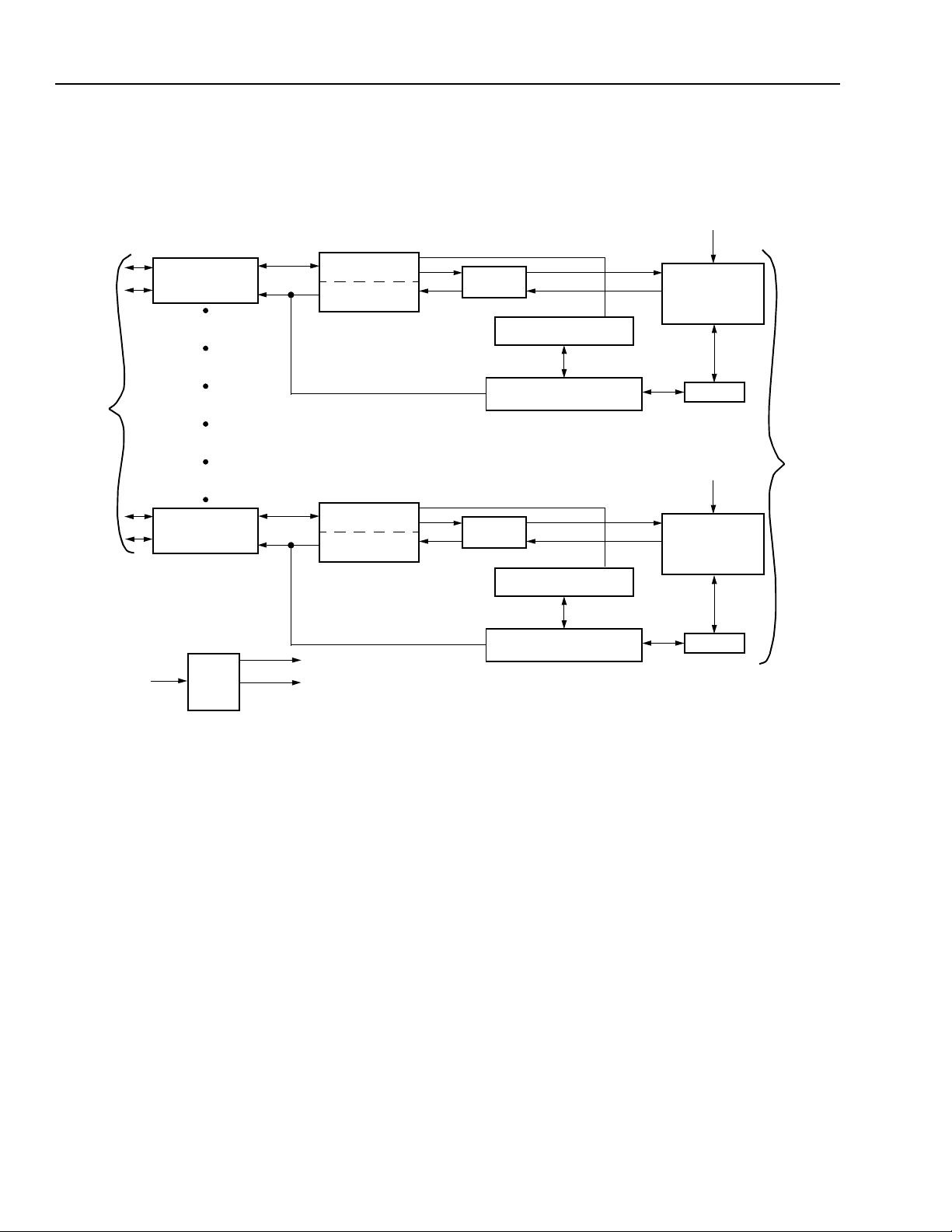
Figure 1. 3X38 Device Overview..............................................................................................................................................................6
Figure 2. 3X38 Single-Channel Detail Functions.....................................................................................................................................7
Figure 3. Typical Single-Channel Twisted-Pair (TP) Interface ..................................................................................................................8
Figure 4. Typical Single-Channel Fiber-Optic (FX) Interface....................................................................................................................9
Figure 5. 3X38 Pinout for RMII Mode.....................................................................................................................................................10
Figure 6. 3X38 Pinout for SMII Mode.....................................................................................................................................................11
Figure 7. Functional Description............................................................................................................................................................27
Figure 8. RMII Receive Timing from Internal MII Signals.......................................................................................................................28
Figure 9. SMII Connection Diagram.......................................................................................................................................................29
Figure 10. Receive Sequence Diagram .................................................................................................................................................29
Figure 11. Transmit Sequence Diagram.................................................................................................................................................30
Figure 12. 100Base-X Data Path ...........................................................................................................................................................32
Figure 13. 10Base-T Module Data Path.................................................................................................................................................37
Figure 14. Timing Diagram .....................................................................................................................................................................42
Figure 15. Hardware Reset Configuration..............................................................................................................................................43
Figure 16. System Clock........................................................................................................................................................................57
Figure 17. Management Clock...............................................................................................................................................................57
Figure 18. RMII Receive Timing.............................................................................................................................................................58
Figure 19. RMII Transmit Timing............................................................................................................................................................58
Figure 20. Transmit Timing .....................................................................................................................................................................59
Figure 21. SMII Timing...........................................................................................................................................................................59
Figure 22. Receive Timing .....................................................................................................................................................................60
Figure 23. Reset and Configuration Timing............................................................................................................................................61
Figure 24. PMD Characteristics .............................................................................................................................................................62
4 Lucent Technologies Inc.

Preliminary Data Sheet 3X38FTR 208-Pin SQFP
September 2000 OCTAL-FET for 10Base-T/100Base-TX/FX
Description
RMII Mode
The reduced media independent interface (RMII) is a
low pin count interface specification promulgated by the
RMII consortium. This specification reduces the total
number of pins from 16 for the
face to seven for the RMII. Architecturally, the RMII
specification provides for an additional reconciliation
sublayer on either side of the MII but, in the 3X38, has
been implemented in the absence of the MII.
The management interface (MDIO/MDC) remains identical to that defined in
IEEE
The RMII specification has the following characteristics:
■
It supports 10 Mbits/s and 100 Mbits/s data rates.
■
A single 50 MHz clock reference is sourced from
MAC to PHY or from an external shared source.
■
It provides independent 2-bit wide transmit and
receive data paths.
IEEE
802.3u.
802.3U MII inter-
LED Control
LEDs can be accessed in one of the following modes:
■
Serial mode. In this mode, all of the LEDs are timedivision multiplexed onto one pin, with a second pin
acting as the clock and a third as a strobe. All LEDs
and all channels share the same pins.
■
Parallel mode. In this mode, each LED and each
channel has its own pin. There is a total of four LED
pins per channel for a total of 32 pins.
■
Bicolor mode. In this mode, each channel has two
outputs to control a bicolor LED. One LED can be
used for each port, indicating link and activity.
In all modes, the LEDs can be operated as
follows:
■
LED stretch.
■
LED blink.
■
No stretch or blink.
Clocking
SMII Mode
The serial media independent interface (SMII) is a low
pin count interface specification promulgated by
Cisco
*. This specification reduces the total number of
pins from 16 for the
the SMII. Architecturally, the SMII specification provides for an additional reconciliation sublayer on either
side of the MII but, in the 3X38, has been implemented
in the absence of the MII.
The management interface (MDIO/MDC) remains identical to that defined in
The SMII specification has the following characteristics:
■
It supports 10 Mbits/s and 100 Mbits/s data rates.
■
A single 125 MHz clock reference is sourced from
MAC to PHY or from an external shared source.
■
It provides independent serial transmit and receive
data paths.
IEEE
802.3u MII interface to two for
IEEE
802.3u.
The 3X38 operates with a 50 MHz clock input when in
the RMII mode, and with a 125 MHz clock input when
in the SMII mode.
FX Mode
Each individual port of the 3X38 can be operated in
100Base-FX mode by selecting it through the pin program option (FX_MODE_EN[7:0]), or through the register bit (register 29, bit 0).
When operating in FX mode, the twisted-pair I/O pins
are reused as the fiber-optic transceiver I/O data pins,
and the fiber-optic signal detect (FOSD) inputs are
enabled.
When a port is placed in FX mode, it will automatically
configure the port for 100Base-FX operation (and the
register bit control will be ignored) such that:
■
The far-end fault signaling option will be enabled.
■
The MLT-3 encoding/decoding will be disabled.
■
Scrambler/descrambler will be disabled.
■
Autonegotiation will be disabled.
■
The signal detect inputs will be activated.
■
10Base-T will be disabled.
*
Cisco
is a registered trademark of Cisco Systems.
Lucent Technologies Inc. 5
3X38FTR 208-Pin SQFP Preliminary Data Sheet
OCTAL-FET for 10Base-T/100Base-TX/FX September 2000
Description
Device Overview
RMII/SMII
INTERFAC E
(continued)
PORT 0
RMII/SMII
INTERFAC E
PORT [1—6]
RMII/SMII
INTERFACE
PORT 7
MANAGEMENT
PCS
MANAGEMENT
PCS
PMA
AUTONEGOTIATION
10 Mbits/s TRANSCEIVER
DRIVER AND FILTERS
PMA
AUTONEGOTIATION
FX_MODE_EN
TX PMD/
FX PORT
DRIVER AND
FILTERS
MUX
FX_MODE_EN
TX PMD/
FX PORT
DRIVER AND
FILTERS
INTERFACE
TP MAGNETICS
50 MHz/125 MHz
RMCLK
PLL
25 MHz
125 MHz
10 Mbits/s TRANSCEIVER
DRIVER AND FILTERS
Figure 1. 3X38 Device Overview
MUX
5-6878(F).c
6 Lucent Technologies Inc.
Preliminary Data Sheet 3X38FTR 208-Pin SQFP
September 2000 OCTAL-FET for 10Base-T/100Base-TX/FX
Description
(continued)
Single-Channel Detail Functions
100 Mbits/s TRANSCEIVER
SMII RMII
TXD[1:0]
TX_EN
CRS_DV
RXD[1:0]
RX_ER
TXD
RXD
SYNC
INTERFACE
MTXD[3:0]
RMII/
SMII
TO
MII
RMII/SMII
4B/5B
ENCODER
TX STATE
MACHINE
CAR_STAT
CIM
RXERR_ST
5B/4B
DECODER
FAR-END
FAULT DETECT
10 Mbits/s TRANSCEIVER
FAULT GEN.
SD
COLLISION
FAR-END
DETECT
CARRIER
DETECT
ALIGNER
SCRAMBLER
RX STATE
MACHINE
SD
DESCRAMBLER
SD
PDT
PDR/
DCRU
SD
PMD
TX
PMD
RX
TPOUT
±
TPIN
±
MANAGEMENT
50 MH
INTERFACE
RMCLK
Z
/125 MH
MDC
MDIO
Z
20 MHz
FREQ.
SYNTH.
LC100
LS100
MANAGEMENT
25 MHz
125 MHz
MII
LC10 LS10
AUTONEGOTIATION
AND LINK MONITOR
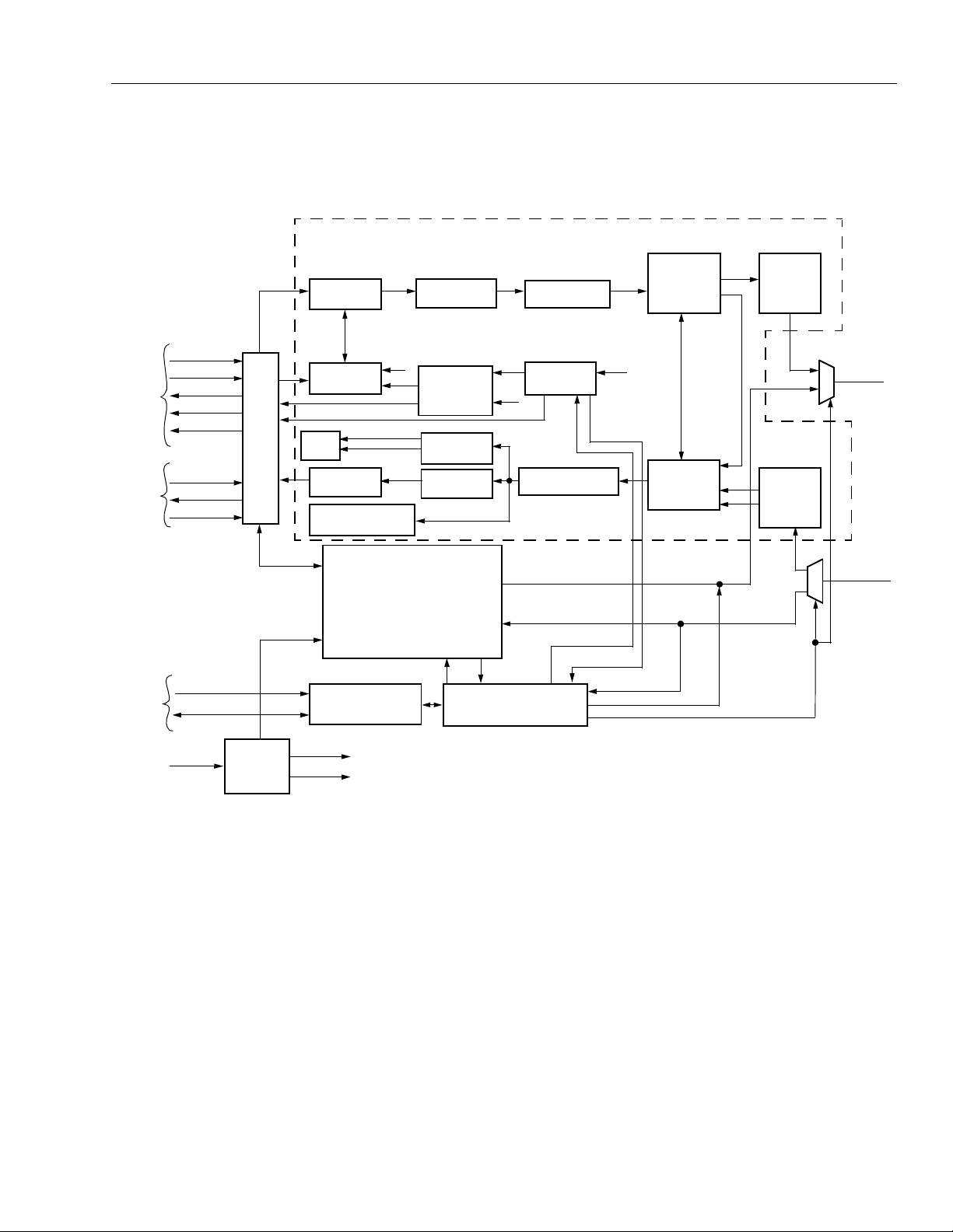
Figure 2. 3X38 Single-Channel Detail Functions
5-5136(F).kr2
Lucent Technologies Inc. 7
3X38FTR 208-Pin SQFP Preliminary Data Sheet
OCTAL-FET for 10Base-T/100Base-TX/FX September 2000
Description
(continued)
Block Diagrams
Single-Channel Twisted-Pair Interface
TPOUT+
6 pF
TPOUT–
3X38
TPIN+
Ω
50
Ω
50
TPIN–
51.1
51.1
DDO
V
1:1
Ω
Ω
0.01 µF
1:1
75
75
Ω
Ω
75
Ω
75
RJ-45
1
2
3
4
5
6
7
8
Ω
0.01 µF
0.01 µF
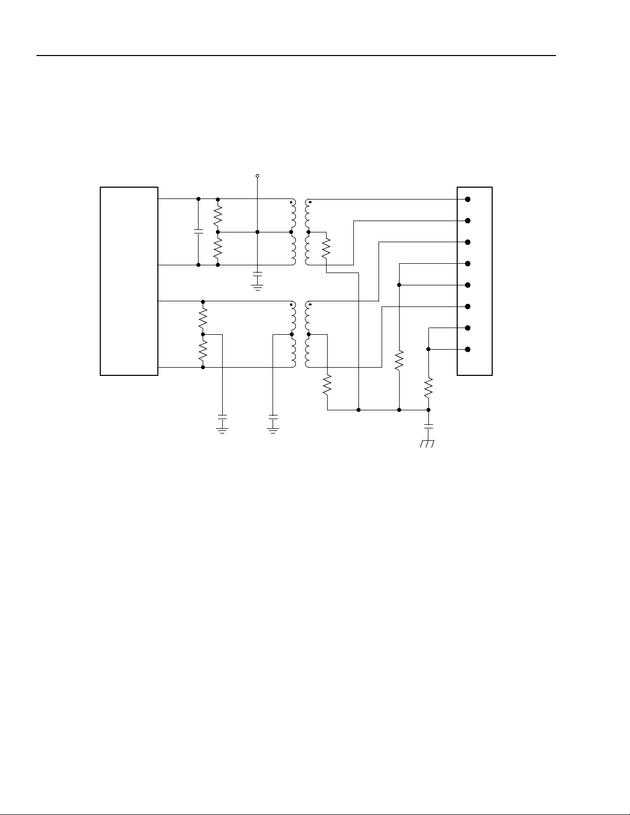
Figure 3. Typical Single-Channel Twisted-Pair (TP) Interface
1000 pF 2 kV
5-5433(F).sr1
8 Lucent Technologies Inc.
Preliminary Data Sheet 3X38FTR 208-Pin SQFP
September 2000 OCTAL-FET for 10Base-T/100Base-TX/FX
Description
(continued)
Single-Channel Fiber-Optic Interface
TPOUT+
Ω
40
Ω
40
TPOUT–
3X38
FOSD
TPIN+
TPIN–
0.01 µF
V
DDO
200
DD
V
0.01 µF
TD
Ω
127
∗
Ω
82.5
∗
Ω
127
82.5
Ω
TDN
SD
RD
RDN
∗
Ω
3.3 V FIBER
TRANSCEIVER
* These terminations per fiber modules recommendation (as shown for
Siemens
†
is a registered trademark of Siemens Aktiegesellschaft.
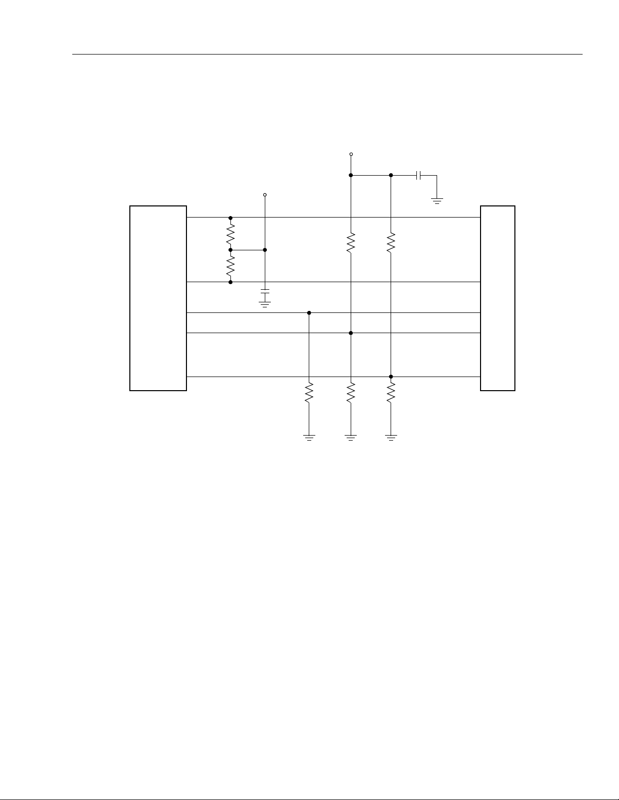
Figure 4. Typical Single-Channel Fiber-Optic (FX) Interface
Siemens
†
V23809-C8-C10).
5-5433(F).qr1
Lucent Technologies Inc. 9

3X38FTR 208-Pin SQFP Preliminary Data Sheet
OCTAL-FET for 10Base-T/100Base-TX/FX September 2000
Pin Information
Pin Diagram for RMII Mode
ACTLED_5/BIACTLED_5/CARIN_EN
ACTLED_3/BIACTLED_3/SCRAM_DESC_BYPASS
ACTLED_4/BIACTLED_4/AUTO_EN
ACTLED_2/BIACTLED_2/LITF_EN
ACTLED_1 /BIA CT LE D_ 1/B LIN K _ LE D_ M O D E
ACTLED_0/BIACTLED_0/STRETCH_LED
RRXD0_7
RRXD1_7
RCRS_DV_7
RRXER_7
RTXD1_7
RTXEN_7
RCRS_DV_6
RRXER_6
RRXD1_6
RRXD0_6
RTXD0_7
RTXD1_6
RTXEN_6
RTXD0_6
RRXD1_5
RCRS_DV_5
RRXER_5
RRXD0_5
RTXD1_5
RTXD0_5
RCRS_DV_4
RTXEN_5
RRXD1_4
RTXD0_4
RRXER_4
RRXD0_4
RTXD1_4
RCRS_DV_3
RTXEN_4
RRXD1_3
RRXD0_3
RTXD0_3
RTXD1_3
RRXER_3
RCRS_DV_2
RTXEN_3
RRXD1_2
RTXD0_2
RRXER_2
RRXD0_2
RTXD1_2
RTXEN_2
ACTLED_6/BIACTLED_6
ACTLED_7/BIACTLED_7
SPEEDLED_0/PHY_ADD[0]
SPEEDLED_1/PHY_ADD[1]
SPEEDLED_2/PHY_ADD[2]
SPEEDLED_3/NO_LP
VDDSPEEDLED_4/LED_MODE0
SPEEDLED_5/LED_MODE1
SPEEDLED_6
SPEEDLED_7
FDUPLED_0/SERCLK/CRS_SEL
208
207
206
205
204
203
202
201
200
199
198
1 156
V
SS
2
3
4
5
6
7
8
9
10
11
12
13
14
15
V
DD
16
17
18
19
20
21
22
23
24
25
26
27
28
29
30
V
DD
31
32
33
34
35
36
37
38
39
40
41
42
43
44
45
V
DD
46
47
48
49
50
51
RMII MODE
52
54555657585960616263646566676869707172737475767778798081828384858687888990919293949596979899100
53
197
FDUPLED_1/SERDATA/FULL_DUP
FDUPLED_2/SE RS TRO B E/ISOL ATE
196
195
VSSVDDVSSV
194
193
192
DDAVDDA
191
DDA
PECP
PECN
ATBON
ATBOP
V
FOSD0
FOSD1
190
189
188
187
186
185
184
183
3X38FTR 208-PIN SQFP
FOSD2
FOSD3
FOSD4
FOSD5
FOSD6
FOSD7
FDUPLED_3/RESERVED
FDUPLED_4/RMII_MODE
VDDFDUPLED_5/SPEED
FDUPLED_6
FDUPLED_7
LINKLED_0/BLINKLED0/FX_MODE_EN0
LINKLED_1/BLINKLED1/FX_MODE_EN1
LINKLED_2/BLINKLED2/FX_MODE_EN2
VDDLINKLED_3/BLINKLED3/FX_MODE_EN3
182
181
180
179
178
177
176
175
174
173
172
171
170
169
168
167
166
LINKLED_4/BLINKLED4/FX_MODE_EN4
165
LINKLED_5/BLINKLED5/FX_MODE_EN5
164
LINKLED_6/BLINKLED6/FX_MODE_EN6
163
LINKLED_7/BLINKLED7/FX_MODE_EN7
162
TDI
VSSVSSVSSV
161
160
101
159
102
158
103
SS
157
155
154
153
152
151
150
149
148
147
146
145
144
143
142
141
140
139
138
137
136
135
134
133
132
131
130
129
128
127
126
125
124
123
122
121
120
119
118
117
116
115
114
113
112
111
110
109
108
107
106
105
104
V
DDA
TPIN+7/FO IN +7
TPIN–7/FO IN–7
V
DDA
TPIN+6/FO IN +6
TPIN–6/FO IN–6
V
DDA
TPIN+5/FO IN +5
TPIN–5/FO IN–5
V
DDA
TPIN+4/FO IN +4
TPIN–4/FO IN–4
V
SS
V
DDA
TPIN+3/FO IN +3
TPIN–3/FO IN–3
V
DDA
TPIN+2/FO IN +2
TPIN–2/FO IN–2
V
DDA
TPIN+1/FO IN +1
TPIN–1/FO IN–1
V
SS
V
DDA
TPIN+0/FO IN +0
TPIN–0/FO IN–0
V
SS
REXTBS
V
DDA
V
DDPLL
RMCLK
V
SS
V
DDA
REXT100
REXT10
V
SS
TPOUT–7/FOOUT–7
TPOUT+7/FOOUT+7
TPOUT–6/FOOUT–6
TPOUT+6/FOOUT+6
TPOUT–5/FOOUT–5
TPOUT+5/FOOUT+5
TPOUT–4/FOOUT–4
TPOUT+4/FOOUT+4
TPOUT–3/FOOUT–3
TPOUT+3/FOOUT+3
TPOUT–2/FOOUT–2
TPOUT+2/FOOUT+2
TPOUT–1/FOOUT–1
TPOUT+1/FOOUT+1
TPOUT–0/FOOUT–0
TPOUT+0/FOOUT+0
SS
DD
V
V
RTXD1_1
RRXD1_1
RTXD0_1
RRXD0_1
RTXEN_1
RRXD1_0
RRXER_1
RCRS_DV_1
RRXD0_0
RRXER_0
RCRS_DV_0
DD
V
O_M
RTXD1_0
RTXEN_0
MDC
MDIO
3-STATE
RTXD0_0
IDDQ
TMODE4
TMODE3
TMODE2
TMODE1
TMODE0
RESET_NOT
SSVSS
SS
SS
SS
SS
SS
SS
DD
V
TCLK
NC
NC
NCNCNC
V
V
TMS
TDO
TRST
NC
V
V
V
SS
NC
NC
NC
V
V
V
MASK_STAT_INT
5-8123(F)
Figure 5. 3X38 Pinout for RMII Mode
10 Lucent Technologies Inc.

Preliminary Data Sheet 3X38FTR 208-Pin SQFP
September 2000 OCTAL-FET for 10Base-T/100Base-TX/FX
Pin Information
(continued)
Pin Diagram for SMII Mode
V
STXD_7
STXD_6
SRXD_7
SRXD_6
STXD_5
SSYNC_7:4
SRXD_5
STXD_4
SRXD_4
STXD_3
SRXD_3
STXD_2
SRXD_2
SSYNC_3:0
SS
NC
NC
NC
NC
NC
V
DD
NC
NC
NC
NC
NC
NC
NC
NC
V
DD
NC
NC
NC
NC
NC
NC
NC
NC
NC
NC
V
DD
NC
NC
NC
NC
NC
ACTLED_5/BIACTLED_5/CARIN_EN
ACTLED_3/BIACTLED_3/ SCR AM _ DES C _B YP AS S
ACTLED_4/BIACTLED_ 4/AU TO_E N
ACTLED_2/BIACTLED_2/LITF_EN
ACTLED_1/BIACTLED_1/B LINK_LE D _M ODE
ACTLED_0/BIACTLED_0/STRETCH_LED
ACTLED_6/BIACTLED_ 6
ACTLED_7/BIACTLED_ 7
SPEEDLED_0/PHY_A D D[0]
SPEEDLED_1/PHY_A D D[1]
SPEEDLED_2/PHY_A D D[2]
SPEEDLED_3/NO_LP
VDDSPEEDLED_4/LED_MODE0
SPEEDLED_5/LED_MODE1
SPEEDLED_6
SPEEDLED_7
FDUPLED_0/SERCLK/CRS_SEL
208
207
206
205
204
203
202
201
200
199
198
1 156
2
3
4
5
6
7
8
9
10
11
12
13
14
15
16
17
18
19
20
21
22
23
24
25
26
27
28
29
30
31
32
33
34
35
36
37
38
39
40
41
42
43
44
45
46
47
48
49
50
51
SMII MODE
52
54555657585960616263646566676869707172737475767778798081828384858687888990919293949596979899100
53
197
DDAVDDA
FDUPLED_1/SERDATA/FULL_DUP
FDUPLED_2/SERSTROBE/ISOLATE
VSSVDDVSSV
196
195
194
193
192
191
DDA
PECP
PECN
ATBON
ATBOP
V
FOSD0
FOSD1
190
189
188
187
186
185
184
183
3X38FTR 208-PIN SQFP
FOSD2
FOSD3
FOSD4
FOSD5
FOSD6
FOSD7
FDUPLED_3/RESERVED
FDUPLED_4/RMII_MODE
VDDFDUPLED_5/SPEED
FDUPLED_6
FDUPLED_7
LINKLED_0/BLINKLED0/FX _M ODE _E N 0
LINKLED_1/BLINKLED1/FX _M ODE _E N 1
LINKLED_2/BLINKLED2/FX _M ODE _E N 2
VDDLINKLED_3/BLINKLED3/FX _M ODE _E N 3
LINKLED_4/BLINKLED4/FX _M ODE _E N 4
LINKLED_5/BLINKLED5/FX _M ODE _E N 5
LINKLED_6/BLINKLED6/FX _M ODE _E N 6
LINKLED_7/BLINKLED7/FX _M ODE _E N 7
TDI
VSSVSSVSSV
182
181
180
179
178
177
176
175
174
173
172
171
170
169
168
167
166
165
164
163
162
161
160
159
158
101
102
103
SS
157
155
154
153
152
151
150
149
148
147
146
145
144
143
142
141
140
139
138
137
136
135
134
133
132
131
130
129
128
127
126
125
124
123
122
121
120
119
118
117
116
115
114
113
112
111
110
109
108
107
106
105
104
V
DDA
TPIN+7/FO IN+7
TPIN–7/FOIN–7
V
DDA
TPIN+6/FO IN+6
TPIN–6/FOIN–6
V
DDA
TPIN+5/FO IN+5
TPIN–5/FOIN–5
V
DDA
TPIN+4/FO IN+4
TPIN–4/FOIN–4
V
SS
V
DDA
TPIN+3/FO IN+3
TPIN–3/FOIN–3
V
DDA
TPIN+2/FO IN+2
TPIN–2/FOIN–2
V
DDA
TPIN+1/FO IN+1
TPIN–1/FOIN–1
V
SS
V
DDA
TPIN+0/FO IN+0
TPIN–0/FOIN–0
V
SS
REXTBS
V
DDA
V
DDPLL
RMCLK
V
SS
V
DDA
REXT100
REXT10
V
SS
TPOUT–7/FOOUT–7
TPOUT+7/FOOUT+7
TPOUT–6/FOOUT–6
TPOUT+6/FOOUT+6
TPOUT–5/FOOUT–5
TPOUT+5/FOOUT+5
TPOUT–4/FOOUT–4
TPOUT+4/FOOUT+4
TPOUT–3/FOOUT–3
TPOUT+3/FOOUT+3
TPOUT–2/FOOUT–2
TPOUT+2/FOOUT+2
TPOUT–1/FOOUT–1
TPOUT+1/FOOUT+1
TPOUT–0/FOOUT–0
TPOUT+0/FOOUT+0
NCNCNC
DD
NC
NC
NC
NC
V
V
STXD_0
SRXD_1
NC
STXD_1
DD
NC
NC
V
O_M
MDC
MDIO
SRXD_0
3-STATE
IDDQ
TMODE4
TMODE3
TMODE2
TMODE1
TMODE0
SS
SSVSS
SS
SS
SS
SS
SS
SS
DD
V
TCLK
NC
NC
NCNCNC
V
V
TMS
TDO
TRST
NC
V
V
V
SS
NC
NC
NC
V
V
V
RESET_NOT
MASK_STAT_INT
5-8124(F).r1
Figure 6. 3X38 Pinout for SMII Mode
Lucent Technologies Inc. 11

3X38FTR 208-Pin SQFP Preliminary Data Sheet
OCTAL-FET for 10Base-T/100Base-TX/FX September 2000
Pin Information
(continued)
Table 1. 3X38 Signal in Alphanumeric Sequence According to Pin Number
Name RMII Mode Name SMII Mode Name
1V
SS
V
SS
2 ACTLED_5 ACTLED_5
3 ACTLED_4 ACTLED_4
4 ACTLED_3 ACTLED_3
5 ACTLED_2 ACTLED_2
6 ACTLED_1 ACTLED_1
7 ACTLED_0 ACTLED_0
8 RRXD0_7 NC
9 RRXD1_7 NC
10 RCRS_DV_7 STXD_7
11 RRXER_7 NC
12 RTXD1_7 NC
13 RTXEN_7 NC
14 RCRS_DV_6 STXD_6
15 V
DD
V
DD
16 RRXER_6 NC
17 RRXD1_6 NC
18 RRXD0_6 NC
19 RTXD0_7 SRXD_7
20 RTXD1_6 NC
21 RTXEN_6 NC
22 RTXD0_6 SRXD_6
23 RRXD1_5 NC
24 RCRS_DV_5 STXD_5
25 RRXER_5 SSYNC_7:4
26 RRXD0_5 NC
27 RTXD1_5 NC
28 RTXD0_5 SRXD_5
29 RCRS_DV_4 STXD_4
30 V
DD
V
DD
31 RTXEN_5 NC
32 RRXD1_4 NC
33 RTXD0_4 SRXD_4
34 RRXER_4 NC
35 RRXD0_4 NC
36 RTXD1_4 NC
37 RCRS_DV_3 STXD_3
38 RTXEN_4 NC
39 RRXD1_3 NC
40 RRXD0_3 NC
41 RTXD0_3 SRXD_3
42 RTXD1_3 NC
43 RRXER_3 NC
Name RMII Mode Name SMII Mode Name
44 RCRS_DV_2 STXD_2
45 V
46 RTXEN_3 NC
47 RRXD1_2 NC
48 RTXD0_2 SRXD_2
49 RRXER_2 SSYNC_3:0
50 RRXD0_2 NC
51 RTXD1_2 NC
52 RTXEN_2 NC
53 RRXD1_1 NC
54 RCRS_DV_1 STXD_1
55 RRXD0_1 NC
56 RRXER_1 NC
57 RTXD1_1 NC
58 RTXEN_1 NC
59 RTXD0_1 SRXD_1
60 V
61 RRXD1_0 NC
62 RCRS_DV_0 STXD_0
63 RRXD0_0 NC
64 RRXER_0 NC
65 V
66 RTXD1_0 NC
67 O_M O_M
68 RTXEN_0 NC
69 MASK_STAT_INT MASK_STAT_INT
70 RTXD0_0 SRXD_0
71 V
72 RESET_NOT RESET_NOT
73 3-STATE 3-STATE
74 MDC MDC
75 MDIO MDIO
76 TMODE4 TMODE4
77 TMODE3 TMODE3
78 TMODE2 TMODE2
79 TMODE1 TMODE1
80 TMODE0 TMODE0
81 IDDQ IDDQ
82 V
83 TCLK TCLK
84 TRST TRST
85 TMS TMS
86 TDO TDO
DD
DD
SS
DD
DD
V
DD
V
DD
V
SS
V
DD
V
DD
12 Lucent Technologies Inc.

Preliminary Data Sheet 3X38FTR 208-Pin SQFP
September 2000 OCTAL-FET for 10Base-T/100Base-TX/FX
Pin Information
(continued)
Table 1. 3X38 Signal in Alphanumeric Sequence According to Pin Number
Name RMII Mode Name SMII Mode Name
87 V
88 V
SS
SS
V
SS
V
SS
89 NC NC
90 V
SS
V
SS
91 NC NC
92 V
SS
V
SS
93 NC NC
94 NC NC
95 NC NC
96 V
SS
V
SS
97 NC NC
98 V
SS
V
SS
99 NC NC
100 V
SS
V
SS
101 NC NC
102 V
SS
V
SS
103 NC NC
104 V
SS
V
SS
105 TPOUT+0 TPOUT+0
106 TPOUT–0 TPOUT–0
107 TPOUT+1 TPOUT+1
108 TPOUT–1 TPOUT–1
109 TPOUT+2 TPOUT+2
110 TPOUT–2 TPOUT–2
111 TPOUT+3 TPOUT+3
112 TPOUT–3 TPOUT–3
113 TPOUT+4 TPOUT+4
114 TPOUT–4 TPOUT–4
115 TPOUT+5 TPOUT+5
116 TPOUT–5 TPOUT–5
117 TPOUT+6 TPOUT+6
118 TPOUT–6 TPOUT–6
119 TPOUT+7 TPOUT+7
120 TPOUT–7 TPOUT–7
121 V
SS
V
SS
122 REXT10 REXT10
123 REXT100 REXT100
124 V
125 V
DDA
SS
V
V
DDA
SS
126 RMCLK RMCLK
127 V
128 V
DDPLL
DDA
V
DDPLL
V
DDA
129 REXTBS REXTBS
Name RMII Mode Name SMII Mode Name
130 V
131 TPIN–0 TPIN–0
132 TPIN+0 TPIN+0
133 V
134 V
135 TPIN–1 TPIN–1
136 TPIN+1 TPIN+1
137 V
138 TPIN–2 TPIN–2
139 TPIN+2 TPIN+2
140 V
141 TPIN–3 TPIN–3
142 TPIN+3 TPIN+3
143 V
144 V
145 TPIN–4 TPIN–4
146 TPIN+4 TPIN+4
147 V
148 TPIN–5 TPIN–5
149 TPIN+5 TPIN+5
150 V
151 TPIN–6 TPIN–6
152 TPIN+6 TPIN+6
153 V
154 TPIN–7 TPIN–7
155 TPIN+7 TPIN+7
156 V
157 V
158 V
159 V
160 V
161 TDI TDI
162 LINKLED_7 LINKLED_7
163 LINKLED_6 LINKLED_6
164 LINKLED_5 LINKLED_5
165 LINKLED_4 LINKLED_4
166 LINKLED_3 LINKLED_3
167 V
168 LINKLED_2 LINKLED_2
169 LINKLED_1 LINKLED_1
170 LINKLED_0 LINKLED_0
171 FDUPLED_7 FDUPLED_7
172 FDUPLED_6 FDUPLED_6
(continued)
SS
DDA
SS
DDA
DDA
DDA
SS
DDA
DDA
DDA
DDA
SS
SS
SS
SS
DD
V
V
V
V
V
V
V
V
V
V
V
V
V
V
V
V
SS
DDA
SS
DDA
DDA
DDA
SS
DDA
DDA
DDA
DDA
SS
SS
SS
SS
DD
Lucent Technologies Inc. 13

3X38FTR 208-Pin SQFP Preliminary Data Sheet
OCTAL-FET for 10Base-T/100Base-TX/FX September 2000
Pin Information
(continued)
Table 1. 3X38 Signal in Alphanumeric Sequence According to Pin Number
Name RMII Mode Name SMII Mode Name
173 FDUPLED_5 FDUPLED_5
174 V
DD
V
DD
175 FDUPLED_4 FDUPLED_4
176 FDUPLED_3 FDUPLED_3
177 FOSD7 FOSD7
178 FOSD6 FOSD6
179 FOSD5 FOSD5
180 FOSD4 FOSD4
181 FOSD3 FOSD3
182 FOSD2 FOSD2
183 FOSD1 FOSD1
184 FOSD0 FOSD0
185 V
DDA
V
DDA
186 ATBOP ATBO P
187 ATBON ATBON
188 PECN PECN
189 PECP PECP
190 V
DDA
V
DDA
Name RMII Mode Name SMII Mode Name
191 V
192 V
193 V
194 V
195 FDUPLED_2 FDUPLED_2
196 FDUPLED_1 FDUPLED_1
197 FDUPLED_0 FDUPLED_0
198 SPEEDLED_7 SPEEDLED_7
199 SPEEDLED_6 SPEEDLED_6
200 SPEEDLED_5 SPEEDLED_5
201 SPEEDLED_4 SPEEDLED_4
202 V
203 SPEEDLED_3 SPEEDLED_3
204 SPEEDLED_2 SPEEDLED_2
205 SPEEDLED_1 SPEEDLED_1
206 SPEEDLED_0 SPEEDLED_0
207 ACTLED_7 ACTLED_7
208 ACTLED_6 ACTLED_6
(continued)
DDA
SS
DD
SS
DD
V
DDA
V
V
V
V
SS
DD
SS
DD
14 Lucent Technologies Inc.

Preliminary Data Sheet 3X38FTR 208-Pin SQFP
September 2000 OCTAL-FET for 10Base-T/100Base-TX/FX
Pin Information
(continued)
Pin Maps
Table 2. 3X38 RMII/SMII Pin Map
Pin
Number
70 RTXD0_0 I SRXD_0 O
68 RTXEN_0 I NC —
66 RTXD1_0 I NC —
64 RRXER_0 O NC —
63 RRXD0_0 O NC —
62 RCRS_DV_0 O STXD_0 I
61 RRXD1_0 O NC —
59 RTXD0_1 I SRXD_1 O
58 RTXEN_1 I NC —
57 RTXD1_1 I NC —
56 RRXER_1 O NC —
55 RRXD0_1 O NC —
54 RCRS_DV_1 O STXD_1 I
53 RRXD1_1 O NC —
52 RTXEN_2 I NC —
51 RTXD1_2 I NC —
50 RRXD0_2 O NC —
49 RRXER_2 O SSYNC_3:0 I
48 RTXD0_2 I SRXD_2 O
47 RRXD1_2 O NC —
44 RCRS_DV_2 O STXD_2 I
46 RTXEN_3 I NC —
43 RRXER_3 O NC —
42 RTXD1_3 I NC —
41 RTXD0_3 I SRXD_3 O
40 RRXD0_3 O NC —
39 RRXD1_3 O NC —
37 RCRS_DV_3 O STXD_3 I
38 RTXEN_4 I NC —
36 RTXD1_4 I NC —
35 RRXD0_4 O NC —
34 RRXER_4 O NC —
33 RTXD0_4 I SRXD_4 O
32 RRXD1_4 O NC —
29 RCRS_DV_4 O STXD_4 I
31 RTXEN_5 I NC —
28 RTXD0_5 I SRXD_5 O
RMII Mode Pins I/O SMII Mode Pins I/O
Lucent Technologies Inc. 15

3X38FTR 208-Pin SQFP Preliminary Data Sheet
OCTAL-FET for 10Base-T/100Base-TX/FX September 2000
Pin Information
Table 2. 3X38 RMII/SMII Pin Map
Pin
Number
27 RTXD1_5 I NC —
26 RRXD0_5 O NC —
25 RRXER_5 O SSYNC_7:4 I
24 RCRS_DV_5 O STX D_5 I
23 RRXD1_5 O NC —
22 RTXD0_6 I SRXD_6 O
21 RTXEN_6 I NC —
20 RTXD1_6 I NC —
18 RRXD0_6 O NC —
17 RRXD1_6 O NC —
16 RRXER_6 O NC —
14 RCRS_DV_6 O STX D_6 I
19 RTXD0_7 I SRXD_7 O
13 RTXEN_7 I NC —
12 RTXD1_7 I NC —
11 RRXER_7 O NC —
10 RCRS_DV_7 O STX D_7 I
9 RRXD1_7 O NC —
8 RRXD0_7 O NC —
175 FDUPLED_4/RMII_MODE
126 RMCLK 50 MHz CLOCK IN I RMCLK 125 MHz CLOCK IN I
(continued)
(continued)
RMII Mode Pins I/O SMII Mode Pins I/O
I FDUPLED_4/SMII_MODE
[TIE LOW]
[TIE HIGH]
I
Pin Descriptions
Table 3. RMII/SMII Interface Pins
Pins Signal Type Description
19, 22, 28, 33,
41, 48, 59, 70
12, 20, 27, 36,
42, 51, 57, 66
13, 21, 31, 38,
46, 52, 58, 68
8, 18, 26, 35,
40, 50, 55, 63
9, 17, 23, 32,
39, 47, 53, 61
16 Lucent Technologies Inc.
RTXD0_[7:0]/
SRXD_[7:0]
RTXD1_[7:0] I
RTXEN_[7:0] I
RRXD0_[7:0] O
RRXD1_[7:0] O
RMII Transmit Data 0
I
nously with RMCLK.
SMII Receive Data and Control
O
tions synchronously with RMCLK.
RMII Transmit Data 1
nously with RMCLK.
RMII Transmit Enable
presenting dibits on RTXD[1:0] for transmission.
RMII Receive Data 0
nously with RMCLK.
RMII Receive Data 1
nously with RMCLK.
. Transmit data bit zero, transitions synchro-
. Receive data and control transi-
. Transmit data bit one, transitions synchro-
. Transmit enable indicates that the MAC is
. Receive data bit zero, transitions synchro-
. Receive data bit one, transitions synchro-

Preliminary Data Sheet 3X38FTR 208-Pin SQFP
September 2000 OCTAL-FET for 10Base-T/100Base-TX/FX
Pin Descriptions
Table 3. RMII/SMII Interface Pins
Pins Signal Type Description
10, 14, 24, 29,
37, 44, 54, 62
11, 16, 34, 43,
56, 64
49 RRXER_2/
25 RRXER_5/
(continued)
RCRS_DV_[7:0]/
STXD_[7:0]
RRXER_[7, 6, 4,
3, 1, 0]
SSYNC_3:0
SSYNC_7:4
(continued)
O
I
O
O
I
O
I
RMII Carrie r Sens e and Re ceiv e Data Valid
asserted when valid data is being received. This signal is asserted
asynchronously.
SMII Transmit Data and Control
nously with the RMCLK.
RMII Receive Error
clock periods to indicate that a coding error or other error was
detected in the frame presently being transferred.
RMII Receive Error
clock periods to indicate that a coding error or other error was
detected in the frame presently being transferred.
SMII Sync
boundaries between each receive data and control 10-bit segments. This input generates a sync pulse every 10 clock cycles.
RMII Receive Error
clock periods to indicate that a coding error or other error was
detected in the frame presently being transferred.
SMII Sync
boundaries between each receive data and control 10-bit segments. There is a sync pulse once every 10 clock cycles.
. Synchronization input to the 3X38 that segments the
. Synchronization input to the 3X38 that segments the
. Receive error is asserted for one or more
. Receive error is asserted for one or more
. Receive error is asserted for one or more
. The CRS_DV will be
. This signal transitions synchro-
Table 4. MII Management
Pins Signal Type Description
74 MDC I
75 MDIO I/O
69 MASK_STAT_INT O
Management Data Clock
transfer of data on the MDIO signal. This signal may be asynchronous to RMCLK. The maximum clock rate is 12.5 MHz.
When running MDC above 6.25 MHz, MDC must be synchronous
with RMCLK and have a setup time of 15 ns and a hold time of 5 ns
with respect to RMCLK.
Management Data Input/Output
trol and status information between the 3X38 and the station management. Control information is driven by the station management
synchronous with MDC. Status information is driven by the 3X38
synchronous with MDC. This pin requires an external
1.5 kΩ pull-up resistor.
Maskable Status Interrupt
a change in status as defined in Table 35 (register 31). This is an
open-drain output and requires a 10 kΩ pull-up resistor.
. This is the timing reference for the
. This I/O is used to transfer con-
. This pin will go low whenever there is
Lucent Technologies Inc. 17

3X38FTR 208-Pin SQFP Preliminary Data Sheet
OCTAL-FET for 10Base-T/100Base-TX/FX September 2000
Pin Descriptions
Table 5. 10/100
Pin Signal Type Description
155, 152,
149, 146,
142, 139,
136, 132
154, 151,
148, 145,
141, 138,
135, 131
119, 117,
115, 113,
111, 109,
107, 105
120, 118,
116, 114,
112, 110,
108, 106
177, 178,
179, 180,
181, 182,
183, 184
Mbits/s Twisted-Pair (TP) Interface Pins
(continued)
TPIN+/
FOIN+[7:0]
TPIN–/
FOIN–[7:0]
TPOUT+/
FOOUT+[7:0]
TPOUT–/
FOOUT–[7:0]
FOSD[7:0] I
Receive Data.
I
10 Mbaud Manchester data from magnetics.
Fiber-Optic Data Input.
pseudo-ECL data from fiber transceiver.
Receive Data.
I
10 Mbaud Manchester data from magnetics.
Fiber-Optic Data Input.
pseudo-ECL data from fiber transceiver.
Transmit Data.
O
10 Mbaud Manchester data to magnetics.
Fiber-Optic Data Output.
pseudo-ECL compatible data to fiber transceiver.
Transmit Data.
O
10 Mbaud Manchester data to magnetics.
Fiber-Optic Data Output.
pseudo-ECL compatible data to fiber transceiver.
Fiber-Optic Signal Detect.
whether or not the fiber-optic receive pairs (FOIN±) are receiving
valid signal levels. These inputs are ignored when not in fiber mode
and should be grounded.
Positive differential received 125 Mbaud MLT3, or
Positive differential received 125 Mbaud
Negative differential received 125 Mbaud MLT3 or
Negative differential received 125 Mbaud
Positive differential transmit 125 Mbaud MLT3 or
Negative differential transmit 125 Mbaud MLT3 or
Positive differential transmit 125 Mbaud
Negative differential transmit 125 Mbaud
Pseudo-ECL input signal which indicates
Table 6. LED and Configuration Pins
Pin Signal Type Description
2 ACTLED_5/
BIACTLED_5/
CARIN_EN
Activity LED[5].
O
port 5. 10 mA active-high output.
O
Bicolor Activity LED[5].
mode by pulling both of the LED_MODE[1:0] pins high at powerup or
reset, this output will go high whenever there is either transmit or
receive activity. This output works in conjunction with the link LED outputs to drive a single bicolor LED package, when in bicolor LED mode.
10 mA active-high output.
I
Carrier Integrity Enable.
through a 10 kΩ resistor, it will enable the carrier integrity function of
register 29, bit 3, if station management is unavailable.
This pin has an internal 50 kΩ pull-down resistor for normal operation
(CARIN_EN is disabled). This input and register bits [29.3] are ORed
together.
This pin indicates transmit or receive activity on
When the 3X38 is placed in the bicolor LED
At powerup or reset, if this pin is pulled high
18 Lucent Technologies Inc.

Preliminary Data Sheet 3X38FTR 208-Pin SQFP
September 2000 OCTAL-FET for 10Base-T/100Base-TX/FX
Pin Descriptions
Table 6. LED and Configuration Pins
Pin Signal Type Description
3ACTLED_4/
BIACTLED_4/
AUTO_EN
4ACTLED_3/
BIACTLED_ 3 /
SCRAM_DESC_BYP
ASS
(continued)
(continued)
Activity LED[4].
O
10 mA active-high output.
O
Bicolor Activity LED[4]
mode by pulling both of the LED_MODE[1:0] pins high at powerup or
reset, this output will go high whenever there is either transmit or
receive activity. This output works in conjunction with the link LED outputs to drive a single bicolor LED package, when in bicolor LED mode.
10 mA active-high output.
I
Autonegotiation Enable
through a 10 kΩ resistor, autonegotiation is enabled. Pulsing this pin will
cause autonegotiation to restart. This input has the same function as
register 0, bit 12. This input and the register bit are ANDed together.
This pin has an internal 50 kΩ pull-do wn res isto r; def aul t is auto neg oti ation off.
Activity LED[3].
O
10 mA active-high output.
O
Bicolor Activity LED[3]
mode by pulling both of the LED_MODE[1:0] pins high at powerup or
reset, this output will go high whenever there is either transmit or
receive activity. This output works in conjunction with the link LED outputs to drive a single bicolor LED package, when in bicolor LED mode.
10 mA active-high output.
I
Scrambler/Descrambler Bypass.
used to enable the SCRAM_DESC_BYP ASS function by pulling this pin
high through a 10 kΩ resistor, if station management is unavailable.
This is the same function as register 29, bit 4.
This pin indicates transmit or receive activity on port 4.
. When the 3X38 is placed in the bicolor LED
. At powerup or reset, when this pin is high
This pin indicates transmit or receive activity on port 3.
. When the 3X38 is placed in the bicolor LED
At powerup or reset, this pin may be
This pin has an internal 50 kΩ pull-down resistor for normal operation
(scrambler/descrambler ON). This input and the register bit [29.4] are
ORed together during powerup and reset.
5ACTLED_2/
BIACTLED_2/
LITF_EN
Lucent Technologies Inc. 19
Activity LED[2].
O
10 mA active-high output.
O
Bicolor Activity LED[2]
mode by pulling both of the LED_MODE[1:0] pins high at powerup or
reset, this output will go high whenever there is either transmit or
receive activity. This output works in conjunction with the link LED outputs to drive a single bicolor LED package, when in bicolor LED mode.
10 mA active-high output.
I
Enhanced Link Integrity Test Function.
at powerup or reset through a 10 kΩ resistor, the 3X38 will detect and
change speed from 10 Mbits/s to 100 Mbits/s, when an instantaneous
speed change occurs. This pin is ORed with register 30, bit 6. This pin
has an internal 50 kΩ pull-up resistor; default is LITF_EN enabled.
This pin indicates transmit or receive activity on port 2.
. When the 3X38 is placed in the bicolor LED
When this input is pulled high

3X38FTR 208-Pin SQFP Preliminary Data Sheet
OCTAL-FET for 10Base-T/100Base-TX/FX September 2000
Pin Descriptions
Table 6. LED and Configuration Pins
Pin Signal Type Description
6 ACTLED_1/
BIACTLED_1/
BLINK_LED_MODE
7 ACTLED_0/
BIACTLED_0/
STRETCH_LED
207,
208
206 SPEEDLED_0/
ACTLED_[7:6]/
BIACTLED[7:6]
PHY_ADD[0]
(continued)
(continued)
Activity LED[1].
O
10 mA active-high output.
O
Bicolor Activity LED[1]
mode by pulling both of the LED_MODE[1:0] pins high at powerup or
reset, this output will go high whenever there is either transmit or
receive activity. This output works in conjunction with the link LED outputs to drive a single bicolor LED package, when in bicolor LED mode.
10 mA active-high output.
I
Blink LED Mode.
10 kΩ resistor (and the STRETCH_LED pin is low), the activity LED
output will blink high for 40 ms and low for 40 ms whenever there is
activity. This signal is ORed with register 29, bit 11. This pin has an
internal 50 kΩ pull-down resistor; default is blink mode disabled.
Activity LED[0].
O
10 mA active-high output.
O
Bicolor Activity LED[0]
mode by pulling both of the LED_MODE[1:0] pins high at powerup or
reset, this output will go high whenever there is either transmit or
receive activity. This output works in conjunction with the link LED outputs to drive a single bicolor LED package, when in bicolor LED mode.
10 mA active-high output.
I
Stretch LED M o de.
10 kΩ resistor, this pin enables stretching. When high, the activity LED
output is stretched to 42 ms minimum and 84 ms maximum, unless
BLINK_LED_MODE is high, in which case it blinks 40 ms high and
40 ms low. This pin is ORed with register 29, bit 7. This pin has an internal 50 kΩ pull-up resistor. Default is stretch LED mode enabled.
Activity LED[7:6].
O
7 or 6. 10 mA active-high output.
O
Bicolor Activity LED[7:6]
mode by pulling both of the LED_MODE[1:0] pins high at powerup or
reset, this output will go high whenever there is either transmit or
receive activity. This output works in conjunction with the link LED outputs to drive a single bicolor LED package, when in bicolor LED mode.
10 mA active-high output.
Speed LED[0].
O
3X38. A high on this pin indicates 100 Mbits/s operation. A low indicates
10 Mbits/s operation. 10 mA active-high output.
I
PHY Address 0
PHY address bit 0.
This pin indicates transmit or receive activity on port 1.
. When the 3X38 is placed in the bicolor LED
At powerup or reset, when pulled high through a
This pin indicates transmit or receive activity on port 0.
. When the 3X38 is placed in the bicolor LED
At powerup or reset, when pulled high through a
This pin indicates transmit or receive activity on port
. When the 3X38 is placed in the bicolor LED
This pin indicates the operating speed of port 0 on the
. At powerup or reset, this pin may be used to set the
At powerup or reset, if this pin is pulled high through a 10 kΩ resistor, it
will set PHYADD[0] to a 1. If this pin is pulled low through a 10 kΩ resistor, it will set PHYADD[0] to a 0. This pin has an internal 50 kΩ pulldown resistor.
20 Lucent Technologies Inc.

Preliminary Data Sheet 3X38FTR 208-Pin SQFP
September 2000 OCTAL-FET for 10Base-T/100Base-TX/FX
Pin Descriptions
Table 6. LED and Configuration Pins
Pin Signal Type Description
205 SPEEDLED_1/
PHY_ADD[1]
204 SPEEDLED_2/
PHY_ADD[2]
203 SPEEDLED_3/
NO_LP
200,
201
SPEEDLED_[5:4]/
LED_MODE[1:0]
(continued)
(continued)
Speed LED[1].
O
3X38. A high on this pin indicates 100 Mbits/s operation. A low indicates
10 Mbits/s operation. 10 mA active-high output.
I
PHY Address 1
PHY address bit 1.
If this pin is pulled high through a 10 kΩ resistor, it will set PHYADD[0] to
a 1. If this pin is pulled low through a 10 kΩ resistor, it will set PHYADD[1] to a 0. This pin has an internal 50 kΩ pull-down resistor.
Speed LED[2].
O
3X38. A high on this pin indicates 100 Mbits/s operation. A low indicates
10 Mbits/s operation. 10 mA active-high output.
I
PHY Address 2
PHY address bit 2.
If this pin is pulled high through a 10 kΩ resistor, it will set PHYADD[0] to
a 1. If this pin is pulled low through a 10 kΩ resistor, it will set PHYADD[2] to a 0. This pin has an internal 50 kΩ pull-down resistor.
Speed LED[3].
O
3X38. A high on this pin indicates 100 Mbits/s operation. A low indicates
10 Mbits/s operation. 10 mA active-high output.
I
No Link Pulse Mode
through a 10 kΩ resistor, will allow 10 Mbits/s operation with link pulses
disabled. If the 3X38 is configured for 100 Mbits/s operation, this signal
is ignored. This is the same function as register 30, bit 0. The input and
the register bit are ORed together. This pin has an internal 50 kΩ pulldown resistor, default is normal link pulse mode.
Speed LED[5:4].
O
on the 3X38. A high on this pin indicates 100 Mbits/s operation. A low
indicates 10 Mbits/s operation. 10 mA active-high output.
I
LED Mode [1:0]
pins[1:0] are used to select the LED mode of operation by pulling them
high or low through a 10 kΩ resistor as shown below.
This pin indicates the operating speed of port 1 on the
. At powerup or reset, this pin may be used to set the
This pin indicates the operating speed of port 2 on the
. At powerup or reset, this pin may be used to set the
This pin indicates the operating speed of port 3 on the
. At powerup or rest, pulling this signal high
These pins indicate the operating speed of ports [5:4]
. At powerup or reset, the LED mode configuration
LED Modes
Pin 1
When in serial LED mode, all eight channels’ LED functions will be multiplexed onto one serial LED output stream.
When in bicolor LED mode, each of the eight channels will have two
LED outputs each, to drive a bicolor LED. These pins have internal
50 kΩ pull-down resistors.
198,
199
Lucent Technologies Inc. 21
SPEEDLED_[7:6] O
Speed LED[7:6].
on the 3X38. A high on this pin indicates 100 Mbits/s operation. A low
indicates 10 Mbits/s operation. 10 mA active-high output.
Pin 0 Mode Outputs
0 0 Parallel SPEEDLED_[7:0], FDUPLED[7:0],
LINKLED[7:0], ACTLED[7:0]
0 1 Reserved Reserved
1 0 Serial SERCLK, SERDATA, SERSTROBE
1 1 Bicolor ACTLED[7:0], LINKLED[7:0]
These pins indicate the operating speed of ports [7:6]

3X38FTR 208-Pin SQFP Preliminary Data Sheet
OCTAL-FET for 10Base-T/100Base-TX/FX September 2000
Pin Descriptions
Table 6. LED and Configuration Pins
Pin Signal Type Description
197 FDUPLED_0/
SERCLK/
CRS_SEL
196 FDUPLED_1/
SERDATA/
FULL_DUP
(continued)
(continued)
Full-Duplex LED[0].
O
LED indicator, or as a collision LED indicator, or as a serial LED output.
This out put is only v alid when t he li nk is up . W hen t he li nk is o per ating in
full-duplex mode, this LED output is the full-duplex LED (logic high output). When the link is operating in half-duplex mode, this LED output
becomes the collision LED output (logic high output). 10 mA active-high
output.
O
Serial LED Clock
to clock out the serial LED data, when the serial LED mode is enabled
by pulling the SERIAL_LED_MODE[1] pin high and the
SERIAL_LED_MODE[0] pin low through a 10 kΩ resistor at pow erup or
reset.
I
Carrier Sense Select.
mode of CRS (carrier sense) operation. When this pin is pulled high
through a 10 kΩ resistor, CRS (carrier sense) will be asserted on
receive activity only. This is the same function as register 29, bit 10.
This pin has an internal 50 kΩ pull-down resistor for normal mode operation (default: CRS asserted on transmit or receive activity). This input
and the register bit [29.10] are ORed together during powerup and
reset.
Full-Duplex LED[1].
O
LED indicator, or as a collision LED indicator, or as a serial LED output.
This out put is only v alid when t he li nk is up . W hen t he li nk is o per ating in
full-duplex mode, this LED output is the full-duplex LED (logic high output). When the link is operating in half-duplex mode, this LED output
becomes the collision LED output (logic high output). 10 mA active-high
output.
O
Serial LED Data
LED status information from all eight 3X38 ports. The serial LED mode
is enabled by pulling the SERIAL_LED_MODE_1 pin high through a
10 kΩ resistor, and the SERIAL_MODE_0 pin low at powerup or reset.
I
Full Duplex.
operation for all eight channels by pulling it high through a 10 kΩ resistor, if station management is unavailable. This is the same function as
register 0, bit 8. This pin has an internal 50 kΩ pull-up resistor to default
to full duplex for normal operation. This input and the register bit[0:8]
are ORed together during powerup and reset. This pin is ignored when
autonegotiation is enabled. This pin has an internal 50 kΩ pull-up to
default to full duplex.
At powerup, this pin may be used to select full-duplex
This LED output can operate as the full-duplex
. This is approximately a 1.56 MHz clock output used
At powerup, this pin may be used to select the
This LED output can operate as the full-duplex
. A single serial LED data stream output that contains
22 Lucent Technologies Inc.

Preliminary Data Sheet 3X38FTR 208-Pin SQFP
September 2000 OCTAL-FET for 10Base-T/100Base-TX/FX
Pin Descriptions
Table 6. LED and Configuration Pins
(continued)
(continued)
Pin Signal Type Description
195 FDUPLED_2/
SERSTROBE/
ISOLATE
Full-Duplex LED[2].
O
This LED output can operate as the full-duplex
LED indicator, or as a collision LED indicator, or as a serial LED output.
This output is only valid when the link is up. When the link is operating in
full-duplex mode, this LED output is the full-duplex LED (logic high output). When the link is operating in half-duplex mode, this LED output
becomes the collision LED output (logic high output). 10 mA active-high
output.
O
Serial LED Strobe
. This is a synchronizing strobe for the serial LED
data output stream that goes high at the start of each serial stream,
once every 32 clocks when in serial LED mode.
I
Isolate Mode.
As an input, this pin can be used at powerup or reset to
select the isolate operation mode. If this pin is pulled high through a
10 kΩ resistor, the 3X38 will powerup or reset to the isolate mode. (RMII
and SMII outputs to high-impedance state.)
This pin is internally pulled through a 50 kΩ resistor. The def ault state is
for the 3X38 to powerup or reset in a nonisolate mode. This pin and register bit [0.10] are ORed together during powerup and reset.
173 FDUPLED_5/
SPEED
Full-Duplex LED[5].
O
This LED output can operate as the full-duplex
LED indicator, or as a collision LED indicator, or as a serial LED output.
This output is only valid when the link is up. When the link is operating in
full-duplex mode, this LED output is the full-duplex LED (logic high output). When the link is operating in half-duplex mode, this LED output
becomes the collision LED output (logic high output). 10 mA active-high
output.
I
Speed
. At powerup or reset, this signal can be used to select the operating speed and is the same function as register 0, bit 13. If this signal is
pulled high with a 10 kΩ
nal is pulled low with a 10 kΩ
, it will enable 100 Mbits/s operation. If this sig-
, it will enable 10 Mbits/s operation.
This signal is ignored when autonegotiation is enabled. This signal and
the register bit are ANDed. This pin has an internal 50 kΩ pull-up, to
default to 100TX mode, when autonegoatiation is not enabled.
171,
172
FDUPLED[7:6] O
Full-Duplex LED[7:6].
This LED output can operate as the full-duplex
LED indicator, or as a collision LED indicator, or as a serial LED output.
This output is only valid when the link is up. When the link is operating in
full-duplex mode, this LED output is the full-duplex LED (logic high output). When the link is operating in half-duplex mode, this LED output
becomes the collision LED output (logic high output). 10 mA active-high
output.
176 FDUPLED_3/
RESERVED
Full-Duplex LED[3].
O
This LED output can operate as the full-duplex
LED indicator, or as a collision LED indicator, or as a serial LED output.
This output is only valid when the link is up. When the link is operating in
full-duplex mode, this LED output is the full-duplex LED (logic high output). When the link is operating in half-duplex mode, this LED output
becomes the collision LED output (logic high output). 10 mA active-high
output.
I
Reserved
. Do not pull this pin high at powerup or reset.
Lucent Technologies Inc. 23

3X38FTR 208-Pin SQFP Preliminary Data Sheet
OCTAL-FET for 10Base-T/100Base-TX/FX September 2000
Pin Descriptions
Table 6. LED and Configuration Pins
Pin Signal Type Description
175 FDUPLED_4/
RMII_MODE
162,
163,
164,
165,
166,
168,
169,
170
LINKLED_[7:0]/
BILINKLED[7:0]/
FX_MODE_EN[7:0]
(continued)
(continued)
Full-Duplex LED[4].
O
LED indicator, or as a collision LED indicator, or as a serial LED output.
This out put is only v alid when t he li nk is up . W hen t he li nk is o per ating in
full-duplex mode, this LED output is the full-duplex LED (logic high output). When the link is operating in half-duplex mode, this LED output
becomes the collision LED output (logic high output). 10 mA active-high
output.
I
RMII Mode
reset, this will place the 3X38 in the SMII mode of operation. When
pulled low, the 3X38 will operate in RMII mode. This pin has an internal
50 kΩ pull-down.
Link LED[7:0].
O
active-high output.
O
Bicolor LED[7:0]
writting a one to bit 10 of register 20. This bit will go high whenever the
link is up and there is no transmit or receive activity . This output works in
conjunction with the activity LED when in bicolor mode. This is a 10 mA
active-high output.
I
FX Mode Enable
10 kΩ resistor, this pin will enable the FX mode (10Base-T and
100Base-TX disabled). When pulled low, it will enable 10Base-T and
100Base-TX modes (100Base-FX mode disabled). These pins are
ORed with register 29, bit 0 [29.0].
. When pulled high through a 10 kΩ resistor at powerup or
This LED output can operate as the full-duplex
This pin indicates good link status on port [7:0]. 10 mA
. When the 3X38 is placed in the bicolor LED mode by
. At powerup or reset, when pulled high through a
These pins have internal 50 kΩ pull-down resistors.
Table 7. Table Test Mode Pins
Pin Signal Type Description
186, 187 ATBOP
ATBON
189, 188 PECP
PECN
81 IDDQ I
161 TDI I
86 TDO O
85 TMS I
83 TCLK I
84 TRST I
Reserved.
O
Reserved.
O
resistors control the slew rate of the RMII and SMII outputs.
IDDQ Mode.
low.
Test Data Input.
pled on the rising edge of TCK. When not in JTAG mode, tie low.
Test Data Output.
Updated on the falling edge of TCK. When not in use, leave unconnected.
Test Mode Select.
pin selects the JTAG test mode. When not in use, tie low.
Test Clock.
data tranfers. When unused, tie low.
Test Reset
troller. For normal use, tie low.
Leave these pins unconnected.
Place a 1 kΩ resistor from these pins to ground. These
Reserved for manufacturing test. For normal use, tie
Serial data input to the JTAG TAP controller. Sam-
Serial data output from the JTAG TAP controller.
When pulled high through a 10 kΩ resistor, this
JTAG clock input used to synchronize JT A G control and
. Asynchronous active-low reset input to JTAG tap con-
24 Lucent Technologies Inc.

Preliminary Data Sheet 3X38FTR 208-Pin SQFP
September 2000 OCTAL-FET for 10Base-T/100Base-TX/FX
Pin Descriptions
Table 7. Table Test Mode Pins
Pin Signal Type Description
76, 77,
78, 79, 80
73 3-STATE I
Table 8. Clock, Reset, FOSD, and Special Configuration Pins
Pin Signal Type Description
126 RMCLK I
72 RESET_NOT I
129 REXTBS I
123 REXT100 I
122 REXT10 I
67 O_M I
(continued)
(continued)
TMODE[4:0] I
T est Mode Select
should be tied low for normal operation.
3-state.
normal operation, pull this pin low.
When this pin is high, all digital outputs will be 3-stated. For
. Reserved for manufacturing testing. These pins
RMII/SMII Clock Input
50 MHz in RMII mode, 125 MHz in SMII mode. ±50 ppm, 40%—
60% duty cycle.
Full Chip Reset Not
1 ms. The 3X38 will come out of reset after 2 ms. RMCLK must
remain running during reset.
External Bias Resistor
tor to ground. The parasitic load capacitance must be less than
15 pF.
External Bias Resistor 100
resistor to ground. This sets the 100 Mbits/s TP driver output level.
External Bias Resistor 10
resistor to ground. This sets the 10 Mbits/s TP driver output level.
Reserved
. Tie this pin high through 10 kΩ resistor.
. CMOS input level system clock input.
. Reset must be asserted low for at least
. Connect this pin to a 24.9 kΩ ± 1% resis-
. Connect this pin to a 21.5 kΩ ± 1%
. Connect this pin to a 21.5 kΩ ± 1%
Lucent Technologies Inc. 25

3X38FTR 208-Pin SQFP Preliminary Data Sheet
OCTAL-FET for 10Base-T/100Base-TX/FX September 2000
Pin Descriptions
(continued)
Table 9. Power, Ground, and No Connects
Pin Signal Type Description
124, 127, 128, 133, 137, 140,
V
DDA
143, 147, 150, 153, 156, 185,
190, 191
127 V
15, 30, 45, 60, 71, 82, 167, 174,
DDPLL
V
DD
193, 202
Magnetics Center Taps V
1, 65, 87, 88, 90, 92, 96, 98,
DDO
V
SS
100, 102, 104, 121, 125, 130,
134, 144, 157, 158, 159, 160,
192, 194
89, 91, 93, 94, 95, 97, 99, 101,
NC NC No connects listed here are for RMII mode only . Ma y be
103
PWR Analog power 3.3 V ± 5%.
PWR Phase -locked loop power 3.3 V ± 5%.
PWR Digi tal powe r 3.3 V ± 5%.
PWR TP driver output power 3.3 V ± 5%. Connected to cen-
tral tap of TP driver output transformer and 51 Ω terminating resistor.
GND Ground.
different in SMII mode.
26 Lucent Technologies Inc.

Preliminary Data Sheet 3X38FTR 208-Pin SQFP
y
September 2000 OCTAL-FET for 10Base-T/100Base-TX/FX
■
Functional Description
The 3X38 integrates eight 100Base-X physical sublayers (PHY), 100Base-TX physical medium dependent
(PMD) transceivers, and eight complete 10Base-T
modules into a single chip for both 10 Mbits/s and
100 Mbits/s Ethernet operation. It also supports
100Base-FX operation through external fiber-optic
transceivers. This device provides a reduced media
independent interface (RMII) or serial media independant interface (SMII) to communicate between the
physical signaling and the medium access control
(MAC) layers for both 100Base-X and 10Base-T operations. Additionally , it pro vides a shared MII port for interfacing to repeater devices. The device is capable of
operating in either full-duplex mode or half-duplex
mode in either 10 Mbits/s or 100 Mbits/s operation.
Operational modes can be selected by hardware configuration pins or software settings of management registers, or can be determined by the on-chip
autonegotiation logic.
The 10Base-T section of the device consists of the
10 Mbits/s transceiver module with filters and a
Manchester ENDEC module.
MII registers
■
IEEE
802.3U autonegotiation
Additionally, there is an interface module that converts
the internal MII signals of the PHY to RMII signal pins.
Each of these functional blocks is described below.
Reduced Media Independent Interface (RMII)
This interface reduces the interconnect circuits
between a MAC and PHY. In switch applications, this
protocol helps to reduce the pin count on the switch
ASIC significantly. A regular 16-pin MII reduces to a
6-pin (7 with an optional RXER pin) RMII. The interconnect circuits are the following:
1. RMCLK: A 50 MHz clock.
2. RTXEN.
3. RTXD[1:0].
4. RRXD[1:0].
5. RCRS_D V.
6. RRXER: Mandator
switch.
for the PHY, but optional for the
The 100Base-X section of the device implements the
following functional blocks:
■
100Base-X physical coding sublayer (PCS)
■
100Base-X physical medium attachment (PMA)
■
Twisted-pair transceiver (PMD)
The 100Base-X and 10Base-T sections share the following functional blocks:
■
Clock synthesizer module (CSM)
MAC RMII PHY
MII MAC I/F TO RMII MAC I/F
TXEN
TXD[3:0]
TXER
TXCLK
COL
CRS
RXDV
RXD[3:0]
RXER
RXCLK
Transmit Data Path
The PHY uses the 50 MHz RMCLK as its reference so
that TXC (at the internal MII) and RMCLK maintain a
phase relationship. This helps to avoid elasticity buffers
on the transmit side. On the rising edge of RMCLK,
2-bit data is provided on the RMII RTXD[1:0] when
RTXEN is high. TXD[1:0] are ignored when RTXEN is
deasserted.
RMII PHY I/F TO MII PHY I/F
RTXEN
RTXD[1:0]
RCRS_DV
RRXD[1:0]
RRXER
RREFCLK
TXEN
TXD[3:0]
TXER
TXCLK
COL
CRS
RXDV
RXD[3:0]
RXER
RXCLK
50 MHz
5-7505(F).a
Figure 7. Functional Description
Lucent Technologies Inc. 27

3X38FTR 208-Pin SQFP Preliminary Data Sheet
OCTAL-FET for 10Base-T/100Base-TX/FX September 2000
Functional Description
(continued)
TX 10 Mbits/s Mode
The RMCLK frequency is 10 times the data rate in this
mode; therefore, the value on RTXD[1:0] will be valid
such that RTXD[1:0] may be sampled every tenth
cycle, regardless of the starting cycle within the group.
TX 100 Mbits/s Mode
There will be valid data on RTXD[1:0] for each RMCLK
period when RTXEN i s asserted.
Receive Data Path
RXC (at the internal MII) is derived from the incoming
data and, hence, does not maintain a phase relationship with RMCLK. Therefore, an elasticity buffer is
required on the receive path. The 3X38 provides a
32-bit FIFO (default) to synchronize the receive data to
the system clock. The start of packet latency can be
reduced from 16 bits to 8 bits by writing a 1 to register
20, bit 11. CRS_DV is asserted asynchronously. Preamble is output onto the RMII once the internal signal
RRX_DV is asserted (on the rising edge of the
RMCLK). CRS_DV is deasserted asynchronously with
the fall of RRX_DV, but RCRS_DV keeps toggling as
long as data is being flushed out of the elasticity buffer.
The CRS_DV signal behavior can be modified by register 20, bit 12. When this bit is set to 0, CRS causes
CRS_DV to be asserted. When this bit is set to a 1,
only RX_DV causes RX_DV to be asserted; this
ensures that false carrier events do not propagate
through the MAC connected to the 3X38.
RX 10 Mbits/s Mode
After the assertion of RCRS_DV, the receive data signals, RRXD[1:0], will be 00 until the 10Base-T PHY has
recovered the clock and decoded the receive data.
Since RMCLK is 10 times the data rate in this mode,
the value on RRXD[1:0] will be valid such that it can be
sampled every tenth cycle, regardless of the starting
cycle within the group.
RX 100 Mbits/s Mode
After the assertion of RCRS_DV, the receive data signals, RRXD[1:0] will be 00 until the start-of-stream
(SSD) delimiter has been detected.
Collision Detection
The RMII does not have a collision signal, so all collisions are detected internal to the MAC. This is an AND
function of RTXEN and RCRS derived from RCRS_DV.
RCRS_DV cannot be directly ANDed with RTXEN
because RCRS_DV may toggle at the end of a frame to
provide separation between RCRS and RRXDV.
Receiver Error
The RRX_ER signal is asserted for one or more
RMCLK periods to indicate that an error was detected
within th e current receive frame.
RMCLK
RCRS
RRX_DV
RCRS_DV
CRS
RRXD[1:0] 00 01 01 00
5-7506(F).a
Figure 8. RMII Receive Timing from Internal MII Signals
28 Lucent Technologies Inc.

Preliminary Data Sheet 3X38FTR 208-Pin SQFP
September 2000 OCTAL-FET for 10Base-T/100Base-TX/FX
Functional Description
(continued)
Loopback
During normal operation, RTXD[1:0] and RTXEN will
not be looped back to RCRS_DV and RRXD[1:0].
RMII/SMII Interface
RMII Isolate Mode
The 3X38 also implements an RMII isolate mode that is
controlled by bit 10 of each one of the eight control registers (register 0h). At reset, the 3X38 will initialize this
bit to 0. Setting the bit to a 1 will put the port into RMII
isolate mode.
MULTI-MAC
STXD[1—6]
SRXD[1—6]
When in isolate mode, the specified port on the 3X38
does not respond to packet data present at the
RTXD[1:0] and RTXEN inputs, and presents a high
impedance on the RCRS_DV, RRXER, and RRXD[1:0]
outputs. The 3X38 will continue to respond to all management transactions while the port is in isolate mode.
Serial Media Independent Interface (SMII)
The SMII allows a further reduction in the number of
signals that are required to interface a PHY to a MAC.
There are two global signals, RMCLK and SSYNC, and
two per-port signals, SRXD and STXD. All signals are
synchronous to the 125 MHz clock.
STXD0
SRXD0
3X38
PORT 0
PORT [1—6]
SMII_CLK
SYNC
RXD
STAD7
SRXD7
SSYNC[3:0]
SSYNC[4:7]
CLOCK
125 MHz
REFERENCE CLOCK
PORT 7
5-7507(F).b
Figure 9. SMII Connection Diagram
1234567891011
CRS RX_DV RXD0 RXD1 RXD2 RXD3 RXD4 RXD5 RXD6 RXD7
5-7507(F)
Figure 10. Receive Sequence Diagram
Lucent Technologies Inc. 29

3X38FTR 208-Pin SQFP Preliminary Data Sheet
OCTAL-FET for 10Base-T/100Base-TX/FX September 2000
Functional Description
(continued)
valid in the segment immediately following a frame, and
will remain valid until the first data segment of the next
Receive Path
Receive data and control information are signaled in
frame.
Transmit Data Path
ten bit segments. These ten bit boundaries are delimited by the SYNC signal. The connected MAC should
generate these SYNC pulses every ten clocks. In
100 Mbits/s mode, each segment represents a new
byte of data. In 10 Mbits/s mode, each segment is
repeated ten times, so every ten segments represents
a new byte of data.
Transmit data and control information are signaled in
ten bit segments similar to the receive path. These ten
bit boundaries are delimited by the SYNC signal. The
connected MAC should generate these SYNC pulses
every ten clocks. In 100 Mbits/s mode, each new segment represents a new byte of data. In 10 Mbits/s
mode, each segment is repeated ten times; therefore,
The receive sequence contains all of the information
found on the standard MII receive path.
Out-of-Band Signaling
During an interframe gap, bit RXD5 indicates the validity of the upper nibble of the last byte of data of the previous frame. Bit RXD0 indicates an error detected by
every ten segments represents a new byte of data. The
PHY can sample one of every ten segments.
Collision Detection
The PHY does not directly indicate that a collision has
occurred. It is left up to the MAC to detect the assertion
of both CRS and TXEN.
the PHY in the previous frame. Both of these bits will be
Table 10. Receive Data/Status Encoding
CRS RX_DV RXD0 RXD1 RXD2 RXD3 RXD4 RXD5 RXD6 RXD7
X 0 Rcvr error
in the
previous
frame
Speed:
0 =
10 Mbits/s
1 =
Duplex:
0 = half
1 = full
Link:
0 = no link
1 = good link
Jabber:
0 = OK
1 = detected
Upper nibble
0 = invalid
1 = valid
False carrier:
0 = OK
1 = detected
100 Mbits/s
X 1 One Data Byte (two MII nibbles)
1
1234567891011
SMII_CLK
SYNC
TXD
TXER TXEN TXD0 TXD1 TXD2 TXD3 TXD4 TXD5 TXD6 TXD7
5-7508(F).r1
Figure 11. Transmit Sequence Diagram
30 Lucent Technologies Inc.

Preliminary Data Sheet 3X38FTR 208-Pin SQFP
September 2000 OCTAL-FET for 10Base-T/100Base-TX/FX
Functional Description
(continued)
Media Independent Interface (MII)—Internal
The 3X38 implements
ant MII interface which connects to the MII-RMII module. This module converts the 4-bit MII receive data to
2-bit RMII receive data. Similarly, it converts the 2-bit
RMII transmit data (received from the MAC) to 4-bit MII
transmit data. The following describes the internal MII
functions.
Transmit Data Interface
Each internal MII transmit data interface comprises
seven signals: TXD[3:0] are the nibble size data path,
TXEN signals the presence of data on TXD, TXER indicates substitution of data with the HALT symbol, and
TXCLK carries the transmit clock that synchronizes all
the transmit signals. TXCLK is usually supplied by the
on-chip clock synthesizer.
Receive Data Interface
Each internal MII receive data interface also comprises
seven signals: RXD[3:0] are the nibble size data path,
RXDV signals the presence of data on RXD, RXER
indicates the validity of data, and RXCLK carries the
receive clock. Depending upon the operation mode,
RXCLK signal is generated by the clock recovery module of either the 100Base-X or 10Base-T receiver.
Status Interface
Two internal MII status signals, COL and CRS, are generated in each of the eight channels to indicate collision
status and carrier sense status. COL is asserted asynchronously whenever the respective channel of 3X38 is
transmitting and receiving at the same time in a halfduplex operation mode. CRS is asserted asynchronously whenever there is activity on either the transmitter or the receiver. When CRS_SEL is asserted, CRS
is asserted only when there is activity on the receiver.
Operation Modes
Each channel of the 3X38 supports two operation
modes and an isolate mode as described below.
100 Mbits/s Mode
internal MII operates in nibble mode with a clock rate of
25 MHz. In normal operation, the internal MII data at
RXD[7:0] and TXD[7:0] are 4 bits wide.
10 Mbits/s Mode
tion, the TXCLK and RXCLK operate at 2.5 MHz. The
data paths are 4 bits wide using TXD[7:0] and
IEEE
802.3U Clause 22 compli-
. For 100 Mbits/s operation, the
. For 10 Mbits/s nibble mode opera-
RXD[7:0] signal lines.
MII Isolate Mode
mode that is controlled by bit 10 of each one of the four
control registers (register 0h). At reset, 3X38 will initialize this bit to the logic level transition of the ISOLATE
pin. Setting the bit to a 1 will also put the port in MII isolate mode.
When in isolate mode, the specified port on the 3X38
does not respond to packet data present at TXD[3:0],
TXEN, and TXER inputs and presents a logic zero on
the TXCLK, RXCLK, RXDV, RXER, RXD[3:0], COL,
and CRS outputs. The 3X38 will continue to respond to
all management transactions while the PHY is in isolate mode.
Serial Management Interface (SMI)
The serial management interface is used to obtain status and to configure the PHY. This mechanism corresponds to the MII specifications for 100Base-X (Clause
22) and supports registers 0 through 6. Additional vendor-specific registers are implemented within the range
of 16 to 31. All the registers are described in the Register Information section on page 46.
Management Register Access
The management interface consists of two pins, management data clock (MDC) and management data
input/output (MDIO). The 3X38 is designed to support
an MDC frequency specified up to 12.5 MHz. The
MDIO line is bidirectional and may be shared by up to
32 devices.
The MDIO pin requires a 1.5 kΩ pull-up resistor which,
during IDLE and turnaround periods, will pull MDIO to a
logic one state. Each MII management data frame is
64 bits long. The first 32 bits are preamble consisting of
32 continuous logic one bits on MDIO and 32 corresponding cycles on MDC. Following preamble is the
start-of-frame field indicated by a <01> pattern. The
next field signals the operation code (OP). <10> indicates read from MII management register operation,
and <01> indicates write to MII management register
operation. The next two fields are PHY device address
and MII management register address. Both of them
are 5 bits wide, and the most significant bit is transferred first.
During read operation, a 2-bit turnaround (TA) time
spacing between the register address field and data
field is provided for the MDIO to avoid contention. Following the turnaround time, a 16-bit data stream is read
from or written into the MII management registers of
the 3X38.
. The 3X38 implements an MII isolate
Lucent Technologies Inc. 31

3X38FTR 208-Pin SQFP Preliminary Data Sheet
OCTAL-FET for 10Base-T/100Base-TX/FX September 2000
Functional Description
(continued)
3X38 will respond to management accesses without
preamble, a minimum of one IDLE bit between man-
The 3X38 supports a preamble suppression mode as
indicated by a 1 in bit 6 of the basic mode status register (BMSR, address 01h). If the station management
agement transactions is required as specified in
802.3U.
Interrupt
IEEE
entity (i.e., MAC or other management controller)
determines that all PHYs in the system support preamble suppression by reading a 1 in this bit, then the station management entity need not generate preamble
for each management transaction. The 3X38 requires a
single initialization sequence of 32 bits of preamble following powerup/hardware reset. This requirement is
generally met by the mandatory pull-up resistor on
MDIO or the management access made to determine
whether preamble suppression is supported. While the
The 3X38 implements interrupt capability that can be
used to notify the management station of certain
events . Interrupt requested by any of the eight PHYs is
combined in this pin. It generates an active-high interrupt pulse on the MASK_STAT_INT output pin whenever one of the interrupt status registers (register
address 31) becomes set while its corresponding interrupt mask register is unmasked. Reading the interrupt
status register (register 31) shows the source of the
interrupt and clears the interrupt output signal.
100Base-X Module
The 3X38 implements 100Base-X compliant PCS and PMA and 100Base-TX compliant TP-PMD as illustrated in
Figure 12. Bypass options for each of the major functional blocks within the 100Base-X PCS provide flexibility for
various applications. 100 Mbits/s PHY loopback is included for diagnostic purposes.
RXCLK
FOSD±
RXD[1:0]
CRS_DV
TXEN
TXD[1:0]
MII-TO-RMII CONVERSION
RMII-TO-MII CONVERSION
RXD[3:0]
TXD[3:0]
BYP_ALIGN
CRS
RXDV
RXEN
COL
TXCLK
TXEN
TXER
BYP_4B5B BYP_SCR
4B/5B DECODE
BYP_4B5B
RX STATE MACHINE
TX STATE MACHINE
SCRAMBLER
4B/5B
DECODE
RYP_SCR
BYP_ALIGN MLT-3
DESCRAMBLER
100BASE-X RECEIVER
PARALLEL-TO-SERIAL
SERIAL-TO-PARALLEL
STATE
MACHINE
CLOCK RECOVERY
100M PHY LOOPBACK
10/100
DRIVER
EQUALIZER
TPIN±
TX
TPOUT±
100BASE-X TRANSMITTER
5-7519(F).a.r1
Figure 12. 100Base-X Data Path
32 Lucent Technologies Inc.

Preliminary Data Sheet 3X38FTR 208-Pin SQFP
September 2000 OCTAL-FET for 10Base-T/100Base-TX/FX
Functional Description
(continued)
Symbol Encoder
The symbol encoder converts 4-bit (4B) nibble data
100Base-X Transmitter
The 100Base-X transmitter consists of functional blocks
which convert synchronous 4-bit nibble data, as provided by the internal MII, to a 125 Mbits/s serial data
stream. This data stream may be routed either to the
on-chip twisted-pair PMD for 100Base-TX signaling, or
to an external fiber-optic PMD for 100Base-FX applications. The 3X38 implements the 100Base-X transmit
state machine as specified in the
IEEE
802.3U Standard, Clause 24 and comprises the following functional
blocks in its data path:
■
Symbol encoder
generated by the RMII-MII module into 5-bit (5B) symbols for transmission. This conversion is required to
allow control symbols to be combined with data symbols. Refer to the table below for 4B to 5B symbol mapping.
Following onset of the TXEN signal, the 4B/5B symbol
encoder replaces the first two nibbles of the preamble
from the MAC frame with a /J/K code-group pair
(11000 10001) start-of-stream delimiter (SSD). The
symbol encoder then replaces subsequent 4B codes
with corresponding 5B symbols. Following negation of
the TXEN signal, the encoder substitutes the first two
IDLE symbols with a /T/R code-group pair (01101
■
Scrambler block
■
Parallel/serial converter and NRZ/NRZI encoder
block
00111) end-of-stream delimiter (ESD) and then continuously injects IDLE symbols into the transmit data
stream until the next transmit packet is detected.
Table 11. Symbol Code Scrambler
Symbol
Name
5B Code
[4:0]
4B Code
[3:0]
Interpretation
0 11110 0000 Data 0
1 01001 0001 Data 1
2 10100 0010 Data 2
3 10101 0011 Data 3
4 01010 0100 Data 4
5 01011 0101 Data 5
6 01110 0110 Data 6
7 01111 0111 Data 7
8 10010 1000 Data 8
9 10011 1001 Data 9
A 10110 1010 Data A
B 10111 1011 Data B
C 11010 1100 Data C
D 11011 1101 Data D
E 11100 1110 Data E
F 11101 1111 Data F
I 11111 Undefined IDLE: interstream fill code
J 11000 0101 First start-of-stream delimiter
K 10001 0101 Second start-of-stream delimiter
T 01101 Undefined First end-of-stream delimiter
R 00111 Undefined Second end-of-stream delimiter
H 00100 Undefined Halt: transfer error
V 00000 Undefined Invalid code
V 00001 Undefined Invalid code
V 00010 Undefined Invalid code
V 00011 Undefined Invalid code
V 00101 Undefined Invalid code
Lucent Technologies Inc. 33

3X38FTR 208-Pin SQFP Preliminary Data Sheet
OCTAL-FET for 10Base-T/100Base-TX/FX September 2000
Functional Description
Table 11. Symbol Code Scrambler
Symbol
Name
5B Code
[4:0]
(continued)
(continued)
4B Code
[3:0]
Interpretation
V 00110 Undefined Invalid code
V 01000 Undefined Invalid code
V 01100 Undefined Invalid code
V 10000 Undefined Invalid code
V 11001 Undefined Invalid code
For 100Base-TX applications, the scrambler is required
to control the radiated emissions at the media connector and on the twisted-pair cable.
The 3X38 implements a data scrambler as defined by
the TP-PMD stream cipher function. The scrambler
uses an 11-bit ciphering linear feedback shift register
(LFSR) with the following recursive linear function:
X[n] = X[n – 11] + X[n – 9] (modulo 2)
The output of the LFSR is combined with data from the
encoder via an exclusive-OR logic function. By scrambling the data, the total energy launched onto the cable
is randomly distributed over a wide frequency range.
be generated by an external optical receiver as in a
100Base-FX application.
The receiver block consists of the following functional
blocks:
■
Equalizer
■
Clock recovery module
■
NRZI/NRZ and serial/parallel decoder
■
Descrambler
■
Symbol alignment block
■
Symbol decoder
Parallel-to-Serial and NRZ-to-NRZI Conversion
After the transmit data stream is scrambled, data is
loaded into a shift register and clocked out with a
125 MHz clock into a serial bit stream. The serialized
data is further converted from NRZ-to-NRZI format,
which produces a transition on every logic one and no
transition on logic zero.
Collision Detect
During 100 Mbits/s half-duplex operation, collision condition is detected if the transmitter and receiver become
active simultaneously. Collision detection is indicated
by the COL signal of the internal MII. When the FDUP
LED input configuration is pulled low, the FUDUP LED
outputs are redefined to be COL LED outputs. For fullduplex applications, the COL signal is never asserted.
100Base-X Receiver
The 100Base-X receiver consists of functional blocks
required to recover and condition the 125 Mbits/s
receive data stream. The 3X38 implements the
100Base-X receive state machine diagram as given in
ANSI */IEEE
Standard 802.3U, Clause 24. The
125 Mbits/s receive data stream may originate from the
on-chip, twisted-pair transceiver in a 100Base-TX
application. Alternatively, the receive data stream may
■
Collision detect block
■
Carrier sense block
■
Stream decoder block
Clock Recovery
The clock recovery module accepts 125 Mbits/s scrambled NRZI data stream from either the on-chip
100Base-TX receiver or from an external 100Base-FX
transceiver. The 3X38 uses an onboard digital phaselocked loop (PLL) to extract clock information of the
incoming NRZI data, which is then used to retime the
data stream and set data boundaries.
After power-on or reset, the PLL locks to a free-running
25 MHz clock derived from the external clock source.
When initial lock is achieved, the PLL switches to lock
to the data stream, extracts a 125 MHz clock from the
data, and uses it for bit framing of the recovered data.
NRZI-to-NRZ and Serial-to-Parallel Conversion
The recovered data is converted from NRZI to NRZ.
The data is not necessarily aligned to 4B/5B codegroup’s boundary. XORed by the deciphering LFSR
and descrambled.
*
ANSI
is a registered trademark of the American National Standards
Institute.
34 Lucent Technologies Inc.

Preliminary Data Sheet 3X38FTR 208-Pin SQFP
September 2000 OCTAL-FET for 10Base-T/100Base-TX/FX
Functional Description
Data Descrambling
The descrambler acquires synchronization with the
data stream by recognizing IDLE bursts of 40 or more
bits and locking its decipheri ng linear feedback shift
register (LFSR) to the state of the scrambling LFSR.
Upon achieving synchronization, the incoming data is
XORed by the deciphering LFSR and descrambled.
In order to maintain synchronization, the descrambler
continuously monitors the validity of the unscrambled
data that it generates. To ensure this, a link state monitor and a hold timer are used to constantly monitor the
synchronization status. Upon synchronization of the
descrambler, the hold timer starts a 722 µs countdown.
Upon detection of sufficient IDLE symbols within the
722 µs period, the hold timer will reset and begin a new
countdown. This monitoring operation will continue
indefinitely given a properly operating network connection with good signal integrity. If the link state monitor
does not recognize sufficient unscrambled IDLE symbols within the 722 µs period, the descrambler will be
forced out of the current state of synchronization and
reset in order to reacquire synchronization.
Symbol Alignment
The symbol alignment circuit in the 3X38 determines
code word alignment by recognizing the /J/K delimiter
pair. This circuit operates on unaligned data from the
descrambler. Once the /J/K symbol pair (11000 10001)
is detected, subsequent data is aligned on a fixed
boundary.
Symbol Decoding
The symbol decoder functions as a look-up table that
translates incoming 5B symbols into 4B nibbles. The
symbol decoder first detects the /J/K symbol pair preceded by IDLE symbols and replaces the symbol with
MAC preamble. All subsequent 5B symbols are converted to the corresponding 4B nibbles for the duration
of the entire packet. This conversion ceases upon the
detection of the /T/R symbol pair denoting the end-ofstream delimiter (ESD). The translated data is presented on the RXD[3:0] signal lines with RXD[0] representing the least significant bit of the translated nibble.
Valid Data Signal
The valid data signal (RXDV) indicates that recovered
and decoded nibbles are being presented on the
(continued)
RXD[3:0] outputs synchronous to RXCLK. RXDV is
asserted when the first nibble of translated /J/K is
ready for transfer ov er the internal MII. It remains active
until either the /T/R delimiter is recognized, link test
indicates failure, or no signal is detected. On any of
these conditions, RXDV is deasserted.
Receiver Errors
The RXER signal is used to communicate receiver
error conditions. While the receiver is in a state of holding RXDV asserted, the RXER will be asserted for each
code word that does not map to a valid code-group.
100Base-X Link Monitor
The 100Base-X link monitor function allows the
receiver to ensure that reliable data is being received.
Without reliable data reception, the link monitor will halt
both transmit and receive operations until such time
that a valid link is detected.
The 3X38 performs the link integrity test as outlined in
IEEE
100Base-X (Clause 24) link monitor state diagram. The link status is multiplexed with 10 Mbits/s link
status to form the reportable link status bit in serial
management register 1 and driven to the LNKLED
pins.
When persistent signal energy is detected on the network, the logic moves into a link-ready state after
approximately 500 µs and waits for an enable from the
autonegotiation module. When received, the link-up
state is entered and the transmit and receive logic
blocks become active. Should autonegotiation be disabled, the link integrity logic moves immediately to the
link-up state after entering the link-ready state.
Carrier Sense
Carrier sense (CRS) for 100 Mbits/s operation is
asserted upon the detection of two noncontiguous
zeros occurring within any 10-bit boundary of the
receive data stream.
The carrier sense function is independent of symbol
alignment. In default mode, CRS is asserted during
either packet transmission or reception. When
CRS_SEL is pulled high at powerup or reset, or when
register 29, bit 10 is written to a 1, CRS is asserted
only during packet reception. When the IDLE symbol
pair is detected in the receive data stream, CRS is
deasserted. In repeater mode, CRS is only asserted
due to receive activity. CRS is intended to encapsulate
RXDV.
Lucent Technologies Inc. 35

3X38FTR 208-Pin SQFP Preliminary Data Sheet
OCTAL-FET for 10Base-T/100Base-TX/FX September 2000
Functional Description
Bad SSD Detection
A bad start-of-stream delimiter (bad SSD) is an error
condition that occurs in the 100Base-X receiver if carrier is detected (CRS asserted) and a valid /J/K set of
code-groups (SSD) is not received.
If this condition is detected, then the 3X38 will assert
RXER and present RXD[3:0] = 1110 to the internal MII
for the cycles that correspond to received 5B codegroups until at least two IDLE code-groups are
detected. In addition, the false carrier counter will be
incremented by one. Once at least two IDLE code
groups are detected, RXER and CRS become deasserted.
Far-End Fault Indication
Autonegotiation provides a mechanism for transferring
information from the local station to the link partner that
a remote fault has occurred for 100Base-TX. Since
autonegotiation is not currently specified for operation
over fiber, the far-end fault indication function (FEFI)
provides this capability for 100Base-FX applications.
A remote fault is an error in the link that one station can
detect while the other cannot. An example of this is a
disconnected wire at a station’s transmitter . This station
will be receiving valid data and detect that the link is
good via the link integrity monitor, but will not be able to
detect that its transmission is not propagating to the
other station.
A 100Base-FX station that detects such a remote fault
may modify its transmitted IDLE stream from all ones to
a group of 84 ones followed by a single 0. This is
referred to as the FEFI IDLE pattern.
The FEFI function is controlled by bit 1 of register 29. It
is initialized to 1 (enabled) if the FOSEL pin is at logic
high level during powerup or reset. If the FEFI function
is enabled, the 3X38 will halt all current operations and
transmit the FEFI IDLE pattern when FOSD signal is
deasserted following a good link indication from the link
integrity monitor. If three or more FEFI IDLE patterns
are detected by the 3X38, then bit 4 of the basic mode
status register (address 01) is set to one until read by
management. Additionally, upon detection of far-end
fault, all receive and transmit MII activity is disabled/
ignored.
(continued)
Carrier Integrity Monitor
The carrier integrity monitor (CIM) function protects the
repeater from transient conditions that would otherwise
cause spurious transmission due to a faulty link. This
function is required for repeater applications and is not
specified for switch applications.
The CIM function is controlled by bit 3 of register 29. It
is initialized to 1 (enabled) during powerup or reset. If
the CIM determines that the link is unstable, the 3X38
will not propagate the received data or control signaling
to the MII and will ignore data transmitted via the MII.
The 3X38 will continue to monitor the receive stream
for valid carrier events. The false carrier counter increments each time the link is unstable (bad SSD). Two
back-to-back false carrier events will isolate the PHY,
incrementing the associated isolate counter. Register
21 provides counters of carrier integrity events when
register 20, bit 11 is written to a 1 (the FIFO is in 32-bit
mode).
100Base-TX Transceiver
3X38 implements a TP-PMD compliant transceiver for
100Base-TX operation. The differential transmit driver
is shared by the 10Base-T and 100Base-TX subsystems. This arrangement results in one device that
uses the same external magnetics for both the
10Base-T and the 100Base-TX transmission with simple RC component connections. The individually waveshaped 10Base-T and 100Base-TX transmit signals
are multiplexed in the transmit output driver section.
Transmit Drivers
The 3X38 100Base-TX transmit driver implements ML T3 translation and wave-shaping functions. The rise/fall
time of the output signal is closely controlled to conform
to the target range specified in the ANSI TP-PMD standard.
Twisted-Pair Receiver
For 100Base-TX operation, the incoming signal is
detected by the on-chip, twisted-pair receiver that comprises the differential line receiver, an adaptive equalizer, and baseline wander compensation circuits.
The 3X38 uses an adaptive equalizer which changes
equalizer frequency response in accordance with cable
length. The cable length is estimated based on the
incoming signal behavior. The equalizer tunes itself
automatically for any cable length to compensate for
the amplitude and phase distortions incurred from the
cable.
36 Lucent Technologies Inc.

Preliminary Data Sheet 3X38FTR 208-Pin SQFP
September 2000 OCTAL-FET for 10Base-T/100Base-TX/FX
Functional Description
(continued)
10Base-T Module
The 10Base-T Transceiver Module is
pliant. It includes the receiver, transmitter, collision,
heartbeat, loopback, jabber, waveshaper, and link
integrity functions, as defined in the standard. Figure 13
provides an overview for the 10Base-T module.
TPIN±
RECEIVE
FILTER
IEEE
SMART
SQUELCH
802.3 com-
CLOCK
RECOVERY
The 3X38 10Base-T module is comprised of the following functional blocks:
■
Manchester encoder and decoder
■
Collision detector
■
Link test function
■
Transmit driver and receiver
■
Serial and parallel interface
■
Jabber and SQE test functions
■
Polarity detection and correction
RXCLK
RCRS_DV
RRXD[1:0]
10BASE-T
RECEIVE
PCS
CRS
RXD[3:0]
RXDV
COL
MII-TO-RMII
CONVERTER
RTXEN
TPOUT±
10/100
TX DRIVER
WAVE
SHAPER
10BASE-T
TRANSMIT
PCS
TXEN
TXER
TXD[3:0]
TXCLK
MII-TO-RMII
CONVERTER
RTXD[1:0]
RTXCLK
5-7521(F).b
Figure 13. 10Base-T Module Data Path
Operation Modes
The 3X38 10Base-T module is capable of operating in either half-duplex mode or full-duplex mode. In half-duplex
mode, the 3X38 functions as an
asserted during collisions or jabber events, and the CRS signal is asserted during transmit and receive. In fullduplex mode, the 3X38 can simultaneously transmit and receive data.
Manchester Encoder/Decoder:
goes high and continues as long as the transceiver is in good link state. Transmission ends when the transmit
enable input goes low. The last transition occurs at the center of the bit cell if the last bit is a 1, or at the boundary
of the bit cell if the last bit is 0.
Decoding is accomplished by a differential input receiver circuit and a phase-locked loop that separates the
Manchester-encoded data stream into clock signals and NRZ data. The decoder detects the end of a frame when
no more midbit transitions are detected. Within one and a half bit times after the last bit, carrier sense is deasserted.
IEEE
802.3 compliant transceiver with fully integrated filtering. The COL signal is
Data encoding and transmission begins when the transmit enable input (TXEN)
Lucent Technologies Inc. 37

3X38FTR 208-Pin SQFP Preliminary Data Sheet
OCTAL-FET for 10Base-T/100Base-TX/FX September 2000
Functional Description
Transmit Driver and Receiver:
all the required signal conditioning functions in its
10Base-T block such that external filters are not
required. Only an isolation transformer and impedance
matching resistors are needed for the 10Base-T transmit and receive interface. The internal transmit filtering
ensures that all the harmonics in the transmit signal are
attenuated properly.
Smart Squelch:
ble for determining when valid data is present on the
differential receive. The 3X38 implements an intelligent
receive squelch on the TPI± differential inputs to
ensure that impulse noise on the receive inputs will not
be mistaken for a valid signal. The squelch circuitry
employs a combination of amplitude and timing measurements (as specified in the
standard) to determine the validity of data on the
twisted-pair inputs.
The signal at the start of the packet is checked by the
analog squelch circuit, and any pulses not exceeding
the squelch level (either positive or negative, depending upon polarity) will be rejected. Once this first
squelch level is overcome correctly, the opposite
squelch level must then be exceeded within 150 ns.
Finally, the signal must exceed the original squelch
level within an additional 150 ns to ensure that the input
wavefo rm will not be rejected.
Only after all of these conditions have been satisfied
will a control signal be generated to indicate to the
remainder of the circuitry that valid data is present.
V alid data is considered to be present until the squelch
level has not been generated for a time longer than
200 ns, indicating end of packet. Once good data has
been detected, the squelch levels are reduced to minimize the effect of noise, causing premature end-ofpacket detection. The receive squelch threshold level
can be lowered for use in longer cable applications.
This is achieved by setting bit 4 of register 30.
Carrier Se nse:
receive activity once valid data is detected via the
smart squelch function.
For 10 Mbits/s half-duplex operation, CRS is asserted
during either packet transmission or reception.
For 10 Mbits/s full-duplex operation, the CRS is
asserted only due to receive activity.
In repeater mode, CRS is only asserted due to receive
activity. CRS is deasserted following an end of packet.
The smart squelch circuit is responsi-
Carrier sense (CRS) is asserted due to
(continued)
The 3X38 integrates
IEEE
802.3 10Base-T
Collision Detection:
sion pin. Collision is detected internal to the MAC,
which is generated by an AND function of TXEN and
CRS derived from CRS_DV. CRS_DV cannot be
directly ANDed with TXEN because CRS_DV may toggle at the end of a frame to provide separation between
CRS and RXDV. The internal MII will still generate the
COL signal, but this information is not passed to the
MAC via the RMII.
Link Test Function:
integrity of the connection with the remote end. If valid
link pulses are not received, the link detector disables
the 10Base-T twisted-pair transmitter, receiver, and collision detection functions.
The link pulse generator produces pulses as defined in
the
IEEE
802.3 10Base-T standard. Each link pulse is
nominally 100 ns in duration and is transmitted every
16 ms, in the absence of transmit data.
Automatic Link Polarity Detection:
10Base-T transceiver module incorporates an automatic link polarity detection circuit. The inverted polarity is determined when seven consecutive link pulses of
inverted polarity or three consecutive packets are
received with inverted end-of-packet pulses. If the input
polarity is reversed, the error condition will be automatically corrected and reported in bit 6 of register 28.
The automatic link polarity detection function can be
disabled by setting bit 3 of register 30.
Clock Synthesizer
The 3X38 implements a clock synthesizer that gener ates all the refe rence clocks needed from a single
external frequency source. The clock source must be a
CMOS signal at 50 MHz or 125 MHz ± 100 ppm.
Autonegotiation
The autonegotiation function provides a mechanism for
exchanging configuration information between two
ends of a link segment and automatically selecting the
highest-performance mode of operation supported by
both devices. Fast link pulse (FLP) bursts provide the
signaling used to communicate autonegotiation abilities
between two devices at each end of a link segment. For
further detail re gardin g aut onegot iati on, re f er t o Clause
28 of the
ports four different Ethernet protocols, so the inclusion
of autonegotiation ensures that the highest-performance protocol will be selected based on the ability of
the link partner.
IEEE
The RMII does not have a colli-
A link pulse is used to check the
The 3X38's
802.3u specification. The 3X38 sup-
38 Lucent Technologies Inc.

Preliminary Data Sheet 3X38FTR 208-Pin SQFP
September 2000 OCTAL-FET for 10Base-T/100Base-TX/FX
Functional Description
The autonegotiation function within the 3X38 can be
controlled either by internal register access or by the
use of configuration pins. At powerup and at device
reset, the configuration pins are sampled. If disabled,
autonegotiation will not occur until software enables bit
12 in register 0. If autonegotiation is enabled, the negotiation process will commence immediately.
When autonegotiation is enabled, the 3X38 transmits
the abilities programmed into the autonegotiation
advertisement register at address 04h via FLP bursts.
Any combination of 10 Mbits/s, 100 Mbits/s, halfduplex, and full-duplex modes may be selected. Autonegotiation controls the exchange of configuration
information. Upon successful autonegotiation, the abilities reported by the link partner are stored in the autonegotiation link partner ability register at address 5.
The contents of the autonegotiation link partner ability
register are used to automatically configure to the
highest-performance prot ocol between the loc al and
far-end nodes. Software can determine which mode
has been configured by autonegotiation by compar ing
the contents of register 04h and 05h and then selecting
the technology whose bit is set in both registers of highest priority relative to the following list:
1. 100Base-TX full duplex (highest priority)
2. 100Base-TX half duplex
3. 10Base-T full duplex
4. 10Base-T half duplex (lowest priority)
The basic mode control register at address 00 provides
control of enabling, disabling, and restarting of the
autonegotiation function. When autonegotiation is disabled, the speed selection bit (bit 13) controls switching
between 10 Mbits/s or 100 Mbits/s operation, while the
duplex mode bit (bit 8) controls switching between fullduplex operation and half-duplex operation. The speed
selection and duplex mode bits have no effect on the
mode of operation when the autonegotiation enable bit
(bit 12) is set.
The basic mode status register at address 01h indicates the set of available abilities for technology types
(bits 15 to 11), autonegotiation ability (bit 3), and
extended register capability (bit 0). These bits are hardwired to indicate the full functionality of the 3X38. The
(continued)
BMSR also provides status on:
1. Whether autonegotiat ion is complete (bit 5).
2. Whether the link partner is advertising that a remote
fault has occurred (bit 4).
3. Whether a valid link has been established (bit 2).
The autonegotiation advertisement register at address
04h indicates the autonegotiation abilities to be advertised by the 3X38. All available abilities are transmitted
by default, but any abi lity can be suppre s s e d b y wri tin g
to this register or configuring external pins.
The autonegotiation link partner ability register at
address 05h indicates the abilities of the link partner as
indicated by autonegotiation communication. The contents of this register are considered valid when the
autonegotiation complete bit (bit 5, register address
01h) is set.
The 3X38 contains an enhanced autonegotiation function that can detect instantaneous speed changes from
10 Mbits/s to 100 Mbits/s. This function can be activated by the LITF_EN input pin, or by setting register
30, bit 6 high. Register 31 provides enhanced autonegotiation status information for debugging purposes.
LED Operational Mo des
The 3X38 provides three basic LED output modes of
operation: parallel mode, serial mode, and bicolor LED
mode. The parallel mode provides four LED output signals for each of the eight channels (32 signals total):
activity, link, speed, and full duplex. The serial mode
multiplexes all eight channels LED status information
onto one single serial output stream. The single data
stream, SERDATA, is accompanied with a serial clock,
SERCLK, and a serial LED strobe, SERSTROBE
(three signals total).
The bicolor LED mode provides two LED output signals, BIACTLED [7:0] and BILINKLED [7:0], for each of
the eight channels (16 signals total). These two outputs
are intended to drive a bicolor LED, packaged in one
single LED package. This reduces the total number of
LED packages to one per channel.
Lucent Technologies Inc. 39

3X38FTR 208-Pin SQFP Preliminary Data Sheet
OCTAL-FET for 10Base-T/100Base-TX/FX September 2000
Functional Description
The LED mode of operation is selected at powerup or reset by the LED_MODE [1:0] configuration pins as shown
below.
Table 12. LED Modes
Pin 1 Pin 0 Mode Outputs
0 0 Parallel SPEEDLED_[7:0], FDUPLED[7:0], LINKLED[7:0], ACTLED[7:0]
0 1 Reserved Reserved
1 0 Serial SERCLK, SERDATA, SERSTROBE
1 1 Bicolor ACTLED[7:0], LINKLED[7:0]
Additional LED output control can be obtained by using
the management registers. Each LED can be forced
either high or low via register 20 on a per-channel
basis. Any register 20 bit that is set overrides the LED
value, no matter what mode the device is in. In bicolor
mode, the activity and link LEDs can be set to flash at a
320 ms rate by setting register 20, bit 9 for activity and
bit 8 for link, on a per-channel basis. When flash is
activated, the LED will continuously flash at the 320 ms
rate regardless of the link state or data activity state.
The activity LED output can operate in three different
modes: pulse stretching, pulse blinking, or no stretching or blinking. With no stretching or blinking, the activity LED will light for as long as there is transmit and/or
receive activity only. When pulse stretching is enabled
by pulling the STRETCH_LED pin high at powerup or
reset, or by setting register 29, bit 7 high, the activity
LED will light approximately 42 ms to 84 ms, when
transmit or receive activity is detected. If the blink function is enabled by pulling the BLINK_LED pin high at
powerup or reset, or by setting register 29, bit 11 high,
the activity LED will blink 500 ms on 500 ms off every
time transmit or receive activity is detected. If both
blink and stretch are enabled, the activity LED will blink
2.5 s on 2.5 s off, every time a packet is received.
(continued)
All LED outputs are 10 mA active-high outputs, no
external buffers are required.
Parallel LED Mode
When operating in the parallel LED mode, each channel has four LED outputs: activity, link, speed, and full
duplex/collision. The activity LED can be stretched or
can blink on transmit or receive activity as described
above. Each of these four LEDs can be forced on or off
by using register 20.
Serial LED Mode
When the serial LED mode is selected, the LED status
information from all eight channels is multiplexed into
one serial LED data stream. The activity LED function
can still be stretched or blink as described above and
each LED output can still be forced high or low as
described above.
The 3X38 contains a serial LED mode. This mode is
selected by holding the input LED mode pin 1 high and
the LED mode pin 0 low. This mode is a 3-pin serial
LED mode.
40 Lucent Technologies Inc.

Preliminary Data Sheet 3X38FTR 208-Pin SQFP
September 2000 OCTAL-FET for 10Base-T/100Base-TX/FX
Functional Description
Table 13. Serial LED Pin Descriptions
Signal Type Description
SERLEDCLK Output This is roughly a 1 MHz output clock (25 MHz/16 MHz). All
SERLEDDATA Output This is a serial stream, clocked by SERLED clock. The serial
SERLEDSTROBE Output This is a strobe, which goes high at the start of each serial
Serial Stream Order
Every SERLEDSTROBE indicates a serial LED stream follows. Each serial LED stream consists of the following
components.
Table 14. Serial LED Port Order
Clock #–10123456
Strobe10000000
Data 1 Chnl(4) Chnl(3) Chnl(2) Chnl(1) Chnl(0) Act Link
(continued)
other serial LED signals change 80 ns—200 ns after the falling
edge of this clock. This clock is generated from LEDCLK.
stream contents are discussed below.
stream. A strobe occurs once every 32 clocks.
Clock # 7 8 9 10 11 12 13
Strobe0000000
Data Speed FullDup Coll Jabber APS RS XS
Chnl4:0 is the current PHY channel count (0 = channel 0 (A), 1 = channel 1, . . . , 00101 = channel 5 (F)). All other
signals are discussed above. Note that data always goes high when strobe goes high; thus, if a user wishes to
implement a 2-pin interface using just clock and data, this high pulse can be used for synchronization.
The Chnl4:0 will cycle through each of the PHY addresses from 0 to 7 before starting over. Since the LED strobe
occurs once every 32 clocks, there will be 17 clocks between each data burst. Thus, the data burst looks something like (for PHY channel 0, then channel 1) Figure 14.
Lucent Technologies Inc. 41

3X38FTR 208-Pin SQFP Preliminary Data Sheet
OCTAL-FET for 10Base-T/100Base-TX/FX September 2000
Functional Description
CLK
DATA
STROBE
CLK
DATA
STROBE
CLK
DATA
STROBE
CLK
DATA
STROBE
BPSSARX
CCCCCA LS FC 143210C1PDL
01234567890
CCCCCA LSFC 143210C1PDL
(continued)
11234567890
02345678901
0123456789
5-7897(F).r1
Figure 14. Timing Diagram
Bicolor LED Mode
When bicolor LED mode is selected, the 3X38 provides two LED output signals per channel. These signals are the
activity LED outputs (BIACTLED) and the link LED outputs (BILINKLED). These two signals work together to drive
a single bicolor LED per channel; this is a single LED package with two LEDs connected in parallel with opposite
polarities. Typically, the BIACTLED is connected to the anode of a green LED with the cathode connected to the
BILINKLED output. A yellow LED is connected to the same outputs in the opposite polarity. The truth table is provided below.
Table 15. Bicolor Mode
BIACTLED BILINKLED
Bicolor LED
State
Indicates
00OffNo link
0 1 Green Link up
1 0 Yellow Activity
1 1 Off Undefined
Activity pulse stretching and blinking can be used as described above, as well as forcing the LEDs on, off, or flashing. To enable the bicolor LED forced mode, register 20, bit 10 must be written to a 1, and then register 20, bits 9
and 8 will be activated. When register 20, bit 9 is written to a 1 the BIACTLED (yellow) will flash 320 ms on, 320 ms
off. When register 20, bit 8 is written to a 1, the BILINKLED (green) will flash 320 ms on, 320 ms off. Other register
20 bits can be used to force these LEDs on or off. See register 20 description for details.
42 Lucent Technologies Inc.

Preliminary Data Sheet 3X38FTR 208-Pin SQFP
September 2000 OCTAL-FET for 10Base-T/100Base-TX/FX
Functional Description
(continued)
Table 16. Bicolor LED Mode Descriptions
R20B10 R20B9 R20B8 State
1 x x Bicolor Mode
0 1 0 Continuously Flash Yellow (320 ms on, 320 ms off)
0 0 1 Continuously Flash Green (320 ms on, 320 ms off)
01 1NA
Reset Operation
The 3X38 can be reset either by hardware or software. A hardware reset is accomplished by applying a negative
pulse, with a duration of at least 1 ms to the RESET_NOT pin of the 3X38 during normal operation. The device
does not internally generate a hardware reset during powerup, an external reset pulse will have to be applied. The
3X38 will come out of RESET after 2 ms. A software reset is activated by setting the reset bit in the basic mode
control register (bit 15, register 00h). This bit is self-clearing and, when set, will return a value of 1 until the software
reset operation has completed.
Hardware reset operation samples the pins and initializes all registers to their default values. This process includes
re-evaluation of all hardware-configurable registers. A hardware reset affects all eight PHYs in the device.
A software reset can reset an individual PHY, and it does not latch the external pins but does reset the registers to
their respective default values.
Logic levels on several I/O pins are detected during a hardware reset to determine the initial functionality of 3X38.
Some of these pins are used as output ports after reset operation.
Care must be taken to ensure that the configuration setup will not interfere with normal operation. Dedicated configuration pins can be tied to Vcc or ground directly. Configuration pins multiplexed with logic level output functions
should be either weakly pulled up or weakly pulled down through resistors. Configuration pins multiplexed with LED
outputs should be set up with one of the following circuits shown in Figure 15.
DD
V
R1
R2
I/O PIN
LOGIC 1 CONFIGURATION LOGIC 0 CONFIGURATION
Note: If a resistor value other then 1.5 kΩ is used for the LED current limit resistor the configuration pull-up should also be this value.
R2
I/O PIN
5-6783(F).d
Figure 15. Hardware Reset Configuration
Lucent Technologies Inc. 43

3X38FTR 208-Pin SQFP Preliminary Data Sheet
OCTAL-FET for 10Base-T/100Base-TX/FX September 2000
MII Station Management
Basic Operation
The primary function of station management is to transfer control and status information about the 3X38 to a management entity. This function is accomplished by the MDC clock input, which has a maximum frequency of
12.5 MHz, along with the MDIO signal.
The MII management interface uses MDC and MDIO to physically transport information between the PHY and the
station management entity.
A specific set of registers and their contents (described in Table 18) defines the nature of the information trans-
ferred across the MDIO interface. Frames transmitted on the MII management interface will have the frame structure shown in Table 17. The order of bit transmission is from left to right. Note that reading and writing the
management register must be completed without interruption. The port addresses are set by the PHYADD pins
(see Table 19 for more detail).
Table 17. MII Management Frame Format
Read/Write
(R/W)
R 1. . .1 01 10 AAAAA RRRRR Z0 DDDDDDDDDDDDDDDD Z
W 1. . .1 01 01 AAAAA RRRRR 10 DDDDDDDDDDDDDDDD Z
Table 18. MII Management Frames—Field Descriptions
Field Descriptions
Pre
ST
OP
PHY_ADD
REGAD
TA
DA TA
IDLE
Pre ST OP PHY_ADD REGAD TA DATA IDLE
Preamble
6.
Start of Frame.
Operation Code
transaction is a 01.
PHY Address
bit transmitted and received is the MSB of the address. A station management entity that is
attached to multiple PHY entities must have prior knowledge of the appropriate PHY address for
each entity.
Register Address.
The first register address bit transmitted and received is the MSB of the address.
Turnaround
the data field of a frame, to avoid drive contention on MDIO during a read transaction. During a
write to the 3X38, these bits are driven to 10 by the station. During a read, the MDIO is not driven
during the first bit time and is driven to a 0 by the 3X38 during the second bit time.
Data
being addressed.
IDLE Condition.
be disabled, and the PHY’s pull-up resistor will pull the MDIO line to a logic 1.
. The 3X38 will accept frames with no preamble. This is indicated by a 1 in register 1, bit
The start of frame is indicated by a 01 pattern.
. The operation code for a read transaction is 10. The operation code for a write
. The PHY address is 5 bits, allowing for 32 unique addresses. The first PHY address
The register address is 5 bits, allowing for 32 unique registers within each PHY.
. The turnaround time is a 2-bit time spacing between the register address field, and
. The data field is 16 bits. The first bit transmitted and received will be bit 15 of the register
The IDLE condition on MDIO is a high-impedance state. All three state drivers will
44 Lucent Technologies Inc.

Preliminary Data Sheet 3X38FTR 208-Pin SQFP
September 2000 OCTAL-FET for 10Base-T/100Base-TX/FX
MII Station Management
PHY_ADD[2:0]
These signals set the management addresses and are decoded as follows.
Table 19. PHY Addresses
PHY_ADD[2:0] Port 0 Port 1 Port 2 Port 3 Port 4 Port 5 Port 6 Port 7
000 01234567
001 8 9 10 11 12 13 14 15
010 16 17 18 19 20 21 22 23
011 24 25 26 27 28 29 30 31
100 678910111213
101 12 13 14 15 16 17 18 19
110 18 19 20 21 22 23 24 25
111 00000000
(continued)
Unmanaged Operations
The 3X38 allows the user to set some of the station management functions during powerup or reset by strapping
outputs high or low through weak resistors (10 kΩ). Table 20 shows the functions and their associated output pins.
For detailed information on the functions of these output pins, refer to the section on management registers
described earlier in this data sheet. Also, information on how these output pins should be strapped is discussed in
the pin descriptions section (Table 3 through Table 7).
Table 20. Output Pins
Function (Register/Bit) Pin Internal Pull-Up/Pull-Down
PHY_ADD[2:0] SPEEDLED_[2:0] 50 kΩ down
NO_LP SPEEDLED_3 50 kΩ down
SPEED FDUPLED_5 50 kΩ up
CARIN_EN ACTLED_5 50 kΩ down
SCRAM_DESC_BYPASS ACTLED_3 50 kΩ down
STRETCH_LED ACTLED_0 50 kΩ up
FULL_DUP FDUPLED_1 50 kΩ up
CRS_SEL FDUPLED_0 50 kΩ down
ISOLATE_M OD E FDU PLE D_2 50 kΩ down
FX_MODE_EN[7:0] LINKLED[7:0 ] 50 kΩ down
RESERVED FDUPLED_3 50 kΩ down
AUTO_EN ACTLED_4 50 kΩ down
LIFT_EN ACTLED_2 50 kΩ up
BLINK_LED_MODE ACTLED_1 50 kΩ down
LED_MODE[1:0] SPEEDLED[5:4] 50 kΩ down
RMII_MODE FDUPLED_4 50 kΩ down
Lucent Technologies Inc. 45

3X38FTR 208-Pin SQFP Preliminary Data Sheet
OCTAL-FET for 10Base-T/100Base-TX/FX September 2000
Register Information
Register Descriptions
The MII management 16-bit register set implemented is as follows. The PHY address pins control the management
pins.
Table 21. Summary of Management Registers (MR)
Register
Address
0 MR0 Control 3000h
1 MR1 Status 7849h
2 MR2 PHY Identifier 1 0180h
3 MR3 PHY Identifier 2 BB80h
4 MR4 Autonegotiation Advertisement 01E1h
5 MR5 Autonegotiation Link Partner Ability (base page, next page) 0000
6 MR6 Autonegotiation Expansion 0000
7 MR7 Next Page Transmit 0000
8—19 MR8—MR19 Reserved —
20 MR20 — —
21 MR21 RXER Counter 0000
22—27 MR22—MR27 Reserved —
28 MR28 Device Specific 1 (status) —
29 MR29 Device Specific 2 (100 Mbits/s control) 2080
30 MR30 Device Specific 3 (10 Mbits/s control) 0000
31 MR31 Quick Status Register —
Table 22. MR0—Control Register Bit Descriptions
Bit
*
0.15 (SW_RESET) R/W
0.14 (LOOPBACK) R/W
0.13 (SPEED100) R/W
0.12 (NWAY_ENA) R/W
0.11 (PWRDN) R/W
Symbol Name
†
Type
Reset.
Setting this bit to a 1 will reset the 3X38. All registers will be set to their
default state. This bit is self-clearing. The default is 0.
Loopback.
media. Any receive data will be ignored. The loopback signal path will contain all
circuitry up to, but not including, the PMD. The autonegotiation must be turned off,
and then loopback can be initiated. Transmit data can start 2 ms after loopback is
initiated. The default value is a 0.
Speed Selection.
100 Mbits/s; 0 = 10 Mbits/s). This bit will only affect operating speed when the autonegotiation enable bit (register 0, bit 12) is disabled (0). This bit is ignored when
autonegotiation is enabled (register 0, bit 12). This bit is ANDed with the SPEED
pin signal (V13).
Autonegotiation Enable.
this bit to a 1. The default state is a 1. This bit is ANDed with the AUTO_EN pin during powerup and reset.
Powerdown.
1; both the 10 Mbits/s transceiver and the 100 Mbits/s transceiver will be powered
down. While in the powerdown state, the 3X38 will respond to management transactions. The default state is a 0.
When this bit is set to 1, no data transmission will take place on the
The value of this bit reflects the current speed of operation (1 =
The autonegotiation process will be enabled by setting
The 3X38 may be placed in a low-power state by setting this bit to a
Description
Default
(Hex Code)
* The format for the bit descriptions is as follows: the first number is the register number, the second number is the bit position in the register.
† R = read, W = write, NA = not applicable.
46 Lucent Technologies Inc.

Preliminary Data Sheet 3X38FTR 208-Pin SQFP
September 2000 OCTAL-FET for 10Base-T/100Base-TX/FX
Register Information
Table 22. MR0—Control Register Bit Descriptions
Bit
*
0.10 (ISOLATE) R/W
Type
(continued)
†
Isolate.
(continued)
Description
When this bit is set to a 1, the MII outputs will be brought to the high-
impedance state. The default state is a 0.
0.9 (REDONWAY) R/W
Restart Autonegotiation.
Normally, the autonegotiation process is started at pow-
erup. The process may be restarted by setting this bit to a 1. The default state is a
0. The NWAYDONE bit (register 1, bit 5) is reset when this bit goes to a 1. This bit
is self-cle ared when autonegotiation restarts.
0.8 (FULL_DUP) R/W
Duplex Mode.
This bit reflects the mode of operation (1 = full duplex; 0 = half
duplex). This bit is ignored when the autonegotiation enable bit (register 0, bit 12) is
enabled. The default state is a 0. This bit is ORed with the FULL_DUP pin (W6).
0.7 (COLTST) R/W
Collision Test.
When this bit is set to a 1, the 3X38 will assert the internal COL
signal in response to RTX_EN. This bit has no external effect on the RMII or SMII
pins.
0.6:0 (RESERVED ) NA
* The format for the bit descriptions is as follows: the first number is the register number, the second number is the bit position in the register.
† R = read, W = write, NA = not applicable.
Reserved.
All bits will read 0.
Table 23. MR1—Status Register Bit Descriptions
Bit
*
1.15 (T4ABLE) R
Type
†
100Base-T4 Ability.
Description
This bit will always be a 0.
0: Not able.
1: Able.
1.14 (TXFULDUP) R
100Base-TX Full-Duplex Ability.
This bit will always be a 1.
0: Not able.
1: Able.
1.13 (TXHAFDUP) R
100Base-TX Half-Duplex Ability.
This bit will always be a 1.
0: Not able.
1: Able.
1.12 (ENFULDUP) R
10Base-T Full-Duplex Ability.
This bit will always be a 1.
0: Not able.
1: Able.
1.11 (ENHAFDUP) R
10Base-T Half-Duplex Ability.
This bit will always be a 1.
0: Not able.
1: Able.
1.10:7 (RESERVED) R
1.6 (NO_PA_OK) R
Reserved.
All bits will read as a 0.
Suppress Preamble.
When this bit is set to a 1, it indicates that the 3X38
accepts management frames with the preamble suppressed.
1.5 (NWAYDONE) R
Autonegotiation Complete.
When this bit is a 1, it indicates the autonegotiation
process has been completed. The contents of registers MR4, MR5, MR6, and
MR7 are now valid. The default value is a 0. This bit is reset when autonegotiation is started.
1.4 (REM_FLT) R
Remote Fault.
When this bit is a 1, it indicates a remote fault has been detected.
This bit will remain set until cleared by reading the register. The default is a 0.
1.3 (NWAYABLE) R
Autonegotiation Ability.
When this bit is a 1, it indicates the ability to perform
autonegotiation. The value of this bit is always a 1.
* The format for the bit descriptions is as follows: the first number is the register number, the second number is the bit position in the register.
† R = read, W = write, NA = not applicable.
Lucent Technologies Inc. 47

3X38FTR 208-Pin SQFP Preliminary Data Sheet
OCTAL-FET for 10Base-T/100Base-TX/FX September 2000
Register Information
Table 23. MR1—Status Register Bit Descriptions
Bit
*
1.2 (LSTAT_OK) R
(continued)
Type
†
Link Status.
(continued)
Description
When this bit is a 1, it indicates a valid link has been established.
This bit has a latching function: a link failure will cause the bit to clear and stay
cleared until it has been read via the management interface.
1.1 (JABBER) R
Jabber Detect.
This bit will be a 1 whenever a jabber condition is detected. It will
remain set until it is read, and the jabber condition no longer exists.
1.0 (EXT_ABLE) R
Extended Capability.
This bit indicates that the 3X38 supports the extended
register set (MR2 and beyond). It will always read a 1.
* The format for the bit descriptions is as follows: the first number is the register number, the second number is the bit position in the register.
† R = read.
Table 24. MR2, MR3—PHY Identification Registers (1 and 2) Bit Descriptions
Bit
*
2.15:0 (OUI[3:18]) R
Type
†
Organizationally Unique Identifier.
Description
The third through the twenty-fourth bit of the
OUI assigned to the PHY manufacturer by the
IEEE
are to be placed in bits 2.15:0
and 3.15:10. The value of bits 15:0 is 0180h.
3.15:10 (OUI[19:24]) R
Organizationally Unique Identifier.
The remaining 6 bits of the OUI. The value
for bits 15:10 is 1Dh.
3.9:4 (MODEL[5:0]) R
3.3:0 (VERSION[3:0]) R
* The format for the bit descriptions is as follows: the first number is the register number, the second number is the bit position in the register.
† R = read.
Model Number.
6-bit model number of the device. The model number is 38h.
Revision Number.
The value of the present revision number is 3h.
Table 25. MR4—Autonegotiation Advertisement Register Bit Descriptions
Bit
*
4.15 (NEXT_PAGE) R/W
Type
†
Next Page.
Description
The next page function is activated by setting this bit to a 1. This will
allow the exchange of additional data. Data is carried by optional next pages of
information.
4.14 (ACK) R/W
4.13 (REM_FAULT) R/W
Acknowledge.
Remote Fault.
This bit is the acknowledge bit from the link code word.
When set to 1, the 3X38 indicates to the link partner a remote fault
condition.
4.12:11
NA
Reserved.
These bits will read zero.
(RESER VED )
4.10 (PAUSE) R/W
Pause.
When set to a 1, it indicates that the 3X38 wishes to exchange flow con-
trol information with its link partner.
4.9 (100B ASET4) R/W
4.8 (100BASET_FD) R/W
100Base-T4.
This bit should always be set to 0.
100Base-TX Full Duplex.
If written to 1, autonegotiation will advertise that the
3X38 is capable of 100Base-TX full-duplex operation.
4.7 (100BASETX) R/W
100Base-TX.
If written to 1, autonegotiation will advertise that the 3X38 is capa-
ble of 100Base-TX operation.
4.6 (10BASET_FD) R/W
10Base-T F ull Duple x.
If written to 1, autonegotiation will advertise that the 3X38
is capable of 10Base-T full-dup lex operation.
4.5 (10BASET) R/W
10Base-T.
If written to 1, autonegotiation will advertise that the 3X38 is capable of
10Base-T operation.
4.4:0 (SELECT) R/W
* The format for the bit descriptions is as follows: the first number is the register number, the second number is the bit position in the register.
† R = read, W = write.
Selector Field
. Reset with the value 00001 for
IEEE
802.3.
48 Lucent Technologies Inc.

Preliminary Data Sheet 3X38FTR 208-Pin SQFP
September 2000 OCTAL-FET for 10Base-T/100Base-TX/FX
Register Information
(continued)
Table 26. MR5—Autonegotiation Link Partner Ability (Base Page) Register Bit Descriptions
Bit
*
5.15 (LP_NEXT_PAGE) R
Type
†
Link Partner Next Page.
Description
When this bit is set to 1, it indicates that the link
partner wishes to engage in next page exchange.
5.14 (LP_ACK) R
Link Partner Acknowledge.
When this bit is set to 1, it indicates that the
link partner has successfully received at least three consecutive and consistent FLP bursts.
5.13 (LP_REM_FAULT ) R
Remote Fault.
When this bit is set to 1, it indicates that the link partner has
a fault.
5.12:5 (LP_TECH_ABILITY) R
Technology Ability Field.
This field contains the technology ability of the
link partner. These bits are similar to the bits defined for the MR4 register
(see Table 2 5).
5.4:0 (LP_SELECT) R
* The format for the bit descriptions is as follows: the first number is the register number, the second number is the bit position in the register.
† R = read.
Selector Field.
ner. For
IEEE
This field contains the type of message sent by the link part-
802.3 compliant link partners, this field should read 00001.
Table 27. MR5—Autonegotiation Link Partner (LP) Ability Register (Next Page) Bit Descriptions
Bit
*
Type
5.15 (LP_NEXT_PAGE) R
†
Next Page
. When this bit is set to a logic 0, it indicates that this is the last
Description
page to be transmitted. A logic 1 indicates that additional pages will follow.
5.14 (LP_ACK) R
Acknowledge.
When this bit is set to a logic 1, it indicates that the link
partner has successfully received its partner’s link code word.
5.13 (LP_MES_PAGE) R
Message Page.
This bit is used by the NEXT _PAGE function to differenti-
ate a message page (logic 1) from an unformatted page (logic 0).
5.12 (LP_ACK2) R
Acknowledge 2.
This bit is used by the NEXT_PAGE function to indicate
that a device has the ability to comply with the message (logic 1) or not
(logic 0).
5.11 (LP_TOGGLE) R
Toggle
. This bit is used by the arbitration function to ensure synchronization with the link partner during next page exchange. Logic 0 indicates that
the previous value of the transmitted link code word was logic 1. Logic 1
indicates that the previous value of the transmitted link code word was
logic 0.
5.10:0 (MCF) R
Message/Unformatted Code Field
. With these 11 bits, there are 2048
possible messages. Message code field definitions are described in annex
28C of the
IEEE
802.3U standard.
* The format for the pin descriptions is as follows: the first number is the register number, the second number is the bit position in the register.
† R = read.
Lucent Technologies Inc. 49

3X38FTR 208-Pin SQFP Preliminary Data Sheet
OCTAL-FET for 10Base-T/100Base-TX/FX September 2000
Register Information
(continued)
Table 28. MR6—Autonegotiation Expansion Register Bit Descriptions
Bit
*
6.15:5 (RESERVED) R
6.4 (PAR_DET_FAULT) R/LH
Type
†
Reserved
.
Parallel Detection Fault.
Description
When this bit is set to 1, it indicates that a fault
has been detected in the parallel detection function. This fault is due to
more than one technology detecting concurrent link conditions. This bit
can only be cleared by reading this register.
6.3 (LP_NEXT_PAGE_ABLE) R
Link Partner Next P age Able.
When this bit is set to 1, it indicates that the
link partner supports the next page function.
6.2 (NEXT_PAGE_ABLE) R
Next Page Able.
This bit is set to 1, indicating that this device supports the
NEXT_PAGE function.
6.1 (PAGE_REC) R/LH
Page Received
. When this bit is set to 1, it indicates that a NEXT_PAGE
has been received.
6.0 (LP_NWAY_ABLE) R
Link Partner Autonegotiation Able.
When this bit is set to 1, it indicates
that the link partner is autonegotiation able.
* The format for the bit descriptions is as follows: the first number is the register number, the second number is the bit position in the register.
† R = read, LH = latched high.
Table 29. MR7—Next Page Transmit Register Bit Descriptions
Bit
*
7.15 (NEXT_PAGE) R/W
Type
†
Next Page.
Description
This bit indicates whether or not this is the last next page to be transmitted. When this bit is 0, it indicates that this is the last page. When this bit is 1, it
indicates there is an additional next page.
7.14 (ACK) R
7.13 (MESSAGE) R/W
Acknowledge.
Message Page.
This bit is the acknowledge bit from the link code word.
This bit is used to differentiate a message page from an unformatted page. When this bit is 0, it indicates an unformatted page. When this bit is 1, it
indicates a formatted page.
7.12 (ACK2) R/W
Acknowledge 2.
This bit is used by the next page function to indicate that a device
has the ability to comply with the message. It is set as follows:
■
When this bit is 0, it indicates the device cannot comply with the message.
■
When this bit is 1, it indicates the device will comply with the message.
7.11 (TOGGLE) R
Toggle.
This bit is used by the arbitration function to ensure synchronization with
the link partner during next page exchange. This bit will always take the opposite
value of the toggle bit in the previously exchanged link code word:
■
If the bit is a logic 0, the previous value of the transmitted link code word was a
logic 1.
■
If the bit is a 1, the previous value of the transmitted link code word was a 0.
The initial value of the toggle bit in the first next page transmitted is the inverse of
the value of bit 11 in the base link code word, and may assume a value of 1 or 0.
7.10:0 (MCF) R/W
Message/Unformatted Code Field.
With these 11 bits, there are 2048 possible
messages. Message code field defi nit ion s are desc r ib ed in annex 28C of the
IEEE
802.3U standard.
* The format for the bit descriptions is as follows: the first number is the register number, the second number is the bit position in the register.
† R = read, W = write.
50 Lucent Technologies Inc.

Preliminary Data Sheet 3X38FTR 208-Pin SQFP
September 2000 OCTAL-FET for 10Base-T/100Base-TX/FX
Register Information
(continued)
Table 30. MR20—LED and FIFO Configuration
Bit
*
Signal Type
20.15:13 Reserved R
20.12 ENH_CRS_DV R/W
†
Reserved.
Enhanced CRS_DV
behavior of CRS_DV in 100 Mbits/s mode so that CRS_DV only goes
high if RXDV (receive data va lid) is high. When thi s bit is a 0 (def a ult),
RCRS_DV will go high on CRS assertion. Default = 0.
20.11 FIFO_DEP R/W
FIFO Depth
FIFO depth (16-bit) (for better latency). Default = 0.
20.10 AUTO_MODE R/W
Automatic Mode
1. When the bicolor automatic mode is disabled the forced bicolor
LED mode is entered, such that register 20, bits 9 and 8 are now activated. When in automatic mode (default), the link LED will go low
whenever activity LED is high. Default = 0. This bit is only valid in
bicolor LED mode.
20.9 ACTLED_FLASH R/W
Activity LED Flash
time, when written to a 1. Default = 0. This bit is only valid in bicolor
LED mode, and automatic mode is disabled.
20.8 LINKLED_FLASH R/W
Link LED Flash
when written to a 1. Default = 0. This bit is only valid in bicolor LED
mode, and automatic mode is disabled.
20.7 FDUPLED_ON R/W
20.6 FDUPLED_OFF R/W
FDUPLED On
FDULED Off
overrides this). Default = 0.
20.5 ACTLED_ON R/W
Force ACT On
Default = 0.
20.4 ACTLED_OFF R/W
Force ACT Off
overrides this). Default = 0.
20.3 SPEEDLED_ON R/W
Force Speed On
Default = 0.
20.2 SPEEDLED_OFF R/W
Force Speed Off
on overrides this). Default = 0.
20.1 LINKLED_ON R/W
Force LINKLED On
Default = 0.
20.0 LINKLED_OFF R/W
Force LINKLED Off
(LINKLED on overrides this). Default = 0.
Description
. This bit, when written to a 1, changes the
. 0 = Normal RMII FIFO depth (32-bit) 1 = reduced RMII
. Disable bicolor automatic mode, when written to a
. Force activity LED to flash at 320 ms high/low
. Force link LED to flash at 320 ms high/low time,
. Force FDUPLED on, when written to a 1. Default = 0.
. Force FDUPLED off, when written to a 1 (FDUPLED on
. Force activity LED on, when written to a 1.
. Force activity LED off, when written to a 1 (ACT on
. Force speed LED on, when written to a 1.
. Force speed LED off, when written to a 1 (speed
. Force link LED on, when written to a 1.
. Force link LED on, when written to a 1
* The format for the bit descriptions is as follows: the first number is the register number, the second number is the bit position in the register.
† R = read, W = write.
Table 31. MR21—RXER Counter
Bit
*
Signal Type
21.0 COUNT_MODE W
†
Counter Mode
Description
. This bit, when 0, puts this register in 16-bit counter
mode. When 1, it puts this register in 8-bit counter mode. This bit is
reset to a 0 and cannot be read.
21.15:0 COUNT_16 R
Counter Value 16-bit Mode
. When in 16-bit counter mode, these
maintain a count of RXERs (receiv e errors). It is re set on a re ad operation.
* The format for the bit descriptions is as follows: the first number is the register number, the second number is the bit position in the register.
† R = read, W = write, NA = not applicable.
Lucent Technologies Inc. 51

3X38FTR 208-Pin SQFP Preliminary Data Sheet
OCTAL-FET for 10Base-T/100Base-TX/FX September 2000
Register Information
Table 31. MR21—RXER Counter
Bit
*
21.7:0 COUNT_8 R
Signal Type
(continued)
(continued)
†
Counter Value 8-bit Mode
Description
. When in 8-bit counter mode, these main-
tain a count of RXERs (receive errors). It is reset on a read operation.
21.11:8 FALSE_CARRIER R
False Carrier Count
. When in 8-bit mode, these contain a count of
false carrier events (802.3 Section 27.3.1.5.1). It is reset on a read
operation.
21.15:12 DISCONN R
Disconnect Count
. When in 8-bit mode, these contain a count of disconnect events (Link Unstable 6, 802.3 Section 27.3.1.5.1). It is reset
on a read operation.
* The format for the bit descriptions is as follows: the first number is the register number, the second number is the bit position in the register.
† R = read, W = write.
Table 32. MR28—Device-Specific Register 1 (Status Register) Bit Descriptions
Bit
*
28.15:9 (UNUSED) R
28.8 (BAD_FRM) R/LH
Type
†
Unused.
Bad Frame.
Description
Read as 0.
If this bit is a 1, it indicates a packet has been received without an
SFD . This bit is only valid in 10 Mbits/s mode.
This bit is latching high and will only clear after it has been read or the device has
been reset.
28.7 (CODE) R/LH
Code Violation.
When this bit is a 1, it indicates a Manchester code violation has
occurred. The error code will be output on the RRXD lines. Refer to Table 1 for a
detailed description of the RRXD pin error codes. This bit is only valid in
10 Mbits/s mode.
This bit is latching high and will only clear after it has been read or the device has
been reset.
28.6 (APS) R
Autopolarity Status.
When register 30, bit 3 is a 0 and this bit is a 1, it indicates
the 3X38 has detected and corrected a polarity reversal on the twisted pair.
If the APF_EN bit (register 30, bit 3) is a 0, the reversal will be corrected inside the
3X38. This bit is not valid in 100 Mbits/s operation.
28.5 (DISCON) R/LH
Disconnect.
If this bit is a 1, it indicates a disconnect. This bit will latch high until
read. This bit is only valid in 100 Mbits/s mode.
28.4 (UNLOCKED) R/LH
Unlocked.
Indicates that the TX scrambler lost lock. This bit will latch high until
read. This bit is only valid in 100 Mbits/s mode.
28.3 (RXERR_ST) R/LH
RX Error Status.
Indicates a false carrier. This bit will latch high until read. This bit
is only valid in 100 Mbits/s mode.
28.2 (FRC_JAM) R/LH
Force Jam.
This bit will latch high until read. This bit is only valid in 100 Mbits/s
mode.
28.1 (LNK100UP) R
Link Up 100.
This bit, when set to a 1, indicates a 100 Mbits/s transceiver is up
and operational.
28.0 (LNK10UP) R
Link Up 10.
This bit, when set to a 1, indicates a 10 Mbits/s transceiver is up and
operational.
* The format for the bit descriptions is as follows: the first number is the register number, the second number is the bit position in the register.
† R = read, LH = latched high.
52 Lucent Technologies Inc.

Preliminary Data Sheet 3X38FTR 208-Pin SQFP
September 2000 OCTAL-FET for 10Base-T/100Base-TX/FX
Register Information
Table 33. MR29—Device-Specific Register 2 (100 Mbits/s Control) Bit Descriptions
Bit
*
29.15 (LOCALRST) R/W
29.14 (RST1) R/W
29.13 (RST2) R/W
29.12 (100_OFF) R/W
29.11 (LED_BLINK) R/W
29.10 (CRS_SEL) R/W
29.9 (LINK_ERR) R/W
29.8 (PKT_ERR) R/W
29.7 (PULSE_STR) R/W
29.6 (EDB) R/W
29.5 (SAB) R/W
29.4 (SDB) R/W
29.3 (CARIN_EN) R/W
29.2 (JAM_COL) R/W
29.1 (FEF-EN) R/W
29.0 (FX) R/W
(continued)
†
Type
Description
Management Reset.
this bit will cause the lower 16 registers and registers 28 and 29 to be reset to
their default values. This bit is self-clearing.
Generic Reset 1.
Generic Reset 2.
100 Mbits/s Transmitter Off.
TPIN– high. This bit defaults to 1.
LED Blinking.
the BLINK_LED_MODE pin (T2). Default is 0.
Carrier Sense Select.
is set to a 1. If this bit is set to logic 0, RCRS_DV will by asserted on receive or
transmit. This bit is ORed with the CRS_SEL pin.
Link Error Indication.
RRXD[1:0] of the 3X38 when RRX_ER is asserted on the MII. If it is 0, it will disable this function.
Packet Error Indication Enable.
indicates that the scrambler is not locked, will be reported on receive data outputs of the 3X38 when RRX_ER is asserted on the RMII. When this bit is 0, it will
disable this function.
Pulse Stretching.
output signals will be stretched between approximately 42 ms—84 ms. If this bit
is 0, it will disable this feature. Default state is 0.
Encoder/Decoder Bypass.
to 0 (default).
Symbol Aligner Bypass.
disabled.
Scrambler/Descrambler Bypass.
descrambling functions will be disabled. This bit is ORed with the scrambler/
descrambler bypass pin (U1).
Carrier Integrity Enable.
This bit is ORed with the CARIN_EN pin (U3).
Jam Enable.
Far-End Fault Enable
transmission capability. This capability may only be used if autonegotiation is
disabled. This capability is to be used only with media which does not support
autonegotiation. Setti ng this bit to 1 enables far-end fault detection, and logic 0
will disable the function. Default state is 0.
Fiber-Optic Mode.
T and 100Base-TX disabled). When low, it will enable 10Base-T and 100BaseTX mode. This bit is ORed with FX_MODE_EN pins. This bit defaults to 1.
This mode is no longer supported, keep this bit set to 0 (default).
This is the local management reset bit. Writing a logic 1 to
This register is used for manufacture test only.
This register is used for manufacture test only.
When this bit is set to 0, it forces TPIP low and
This register, when 1, enables LED blinking. This is ORed with
RCRS_DV will be asserted on receive only when this bit
When this bit is a 1, a link error code will be reported on
When this bit is a 1, a packet error code, which
When this bit is set to 1, the activity LED and collision LED
This mode is no longer supported; keep this bit set
When this bit is set to 1, the aligner function will be
When this bit is set to 1, the scrambling/
When this bit is set to a 1, carrier integrity is enabled.
. This bit is used to enable the far-end fault detection and
When this bit is a 1, the 3X38 is in fiber-optic mode (10Base-
* The format for the bit descriptions is as follows: the first number is the register number, the second number is the bit position in the register.
† R = read, W = write.
Lucent Technologies Inc. 53

3X38FTR 208-Pin SQFP Preliminary Data Sheet
OCTAL-FET for 10Base-T/100Base-TX/FX September 2000
Register Information
Table 34. MR30—Device-Specific Register 3 (10 Mbits/s Control) Bit Descriptions
Bit
*
30.15 (Test10TX) R/W
30.14 (RxPLLEn) R/W
30.13 (JAB_DIS) R/W
30.12:7 (UNUSED) R/W
30.6 (LITF_ENH) R/W
30.5 (HBT_EN) R/W
30.4 (ELL_EN) R/W
30.3 (APF_EN) R/W
Type
(continued)
†
10Base-T Transmitter Test
tinuous 10 MHz signal (1111) will be transmitted. This is only meant for testing. Default 0.
10Base-T Low Power Mode Disable
powered up when the link is up. Otherwise, portions of the logic will be powered down when no data is being received to conserve power. Default is 0.
Jabber Disable.
10Base-T receive. Default is 0.
Unused.
Enhanced Link Integrity T est Function.
it will detect and change speed from 10 Mbits/s to 100 Mbits/s when an instantaneous speed change occurs. This is ORed with the LITF_ENH input
(pin T3). Default is 0.
Heartbeat Enable.
enabled. Valid in 10 Mbits/s mode only.
Extended Line Length Enable.
els are reduced from a nominal 435 mV to 350 mV, allowing reception of signals with a lower amplitude. Valid in 10 Mbits/s mode only.
Autopolarity Function Disable.
10 Mbits/s mode, the autopolarity function will determine if the TP link is wired
with a polarity reversal. Default is 0.
Read as 0.
When this bit is 1, disables the jabber function of the
When this bit is a 1, the heartbeat function will be
Description
. When high and 10Base-T is powered up, a con-
. When high, all 10Base-T logic will be
When high, and function is enabled,
When this bit is a 1, the receive squelch lev-
When this bit is a 0 and the 3X38 is in
If there is a polarity reversal, the 3X38 will assert the APS bit (register 28, bit
6) and correct the polarity reversal. If this bit is a 1 and the device is in
10 Mbits/s mode, the reversal will not be corrected.
30.2 (RESERVED) R/W
30.1 (SERIAL _SEL) R/W
30.0 (ENA_NO_LP) R/W
* The format for the bit descriptions is as follows: the first number is the register number, the second number is the bit position in the register.
† R = read, W = write.
Reserved
Serial Select.
selected. When the 3X38 is in 100 Mbits/s mode, this bit will be ignored.
No Link Pulse Mode.
with link pulses disabled. If the 3X38 is configured for 100 Mbits/s operation,
setting this bit will not affect operation.
.
When this bit is set to a 1, 10 Mbits/s serial mode will be
Setting this bit to a 1 will allow 10 Mbits/s operation
54 Lucent Technologies Inc.

Preliminary Data Sheet 3X38FTR 208-Pin SQFP
September 2000 OCTAL-FET for 10Base-T/100Base-TX/FX
Register Information
(continued)
Table 35. MR31—Device-Specific Register 4 (Quick Status) Bit Descriptions
Register/Bit
31.15 (ERROR) R
31.14 (RXERR_ST)/
(LINK_STAT_CHANGE)
31.13 (REM_FLT) R
31.12 (UNLOCKED)/
(JABBER)
31.11 (LSTAT_OK) R
31.10 (PAUSE) R
31.9 (SPEED100) R
31.8 (FULL_DUP) R
31.7 (INT_CONF) R/W
31.6 (INT_MASK) R/W
31.5:3
(LOW_AUTO_STAT E)
31.2:0
(HI_AUTO_STATE)
*
Type
R
R
R
R
†
Receiver Error.
detected. This bit is valid in 100 Mbits/s only. This bit will remain set until cleared by
reading the register. Default is a 0.
False Carrier.
detect state machine has f ound a false carrier . This bit i s v ali d in 10 0 Mbits/s onl y. This
bit will remain set until cleared by reading the register. Default is 0.
Link Status Change.
LINK_STAT_CHANGE bit and goes high whene ver there is a change in link status (bit
[31.11] changes state).
Remote Fault.
bit will remain set until cleared by reading the register. Default is a 0.
Unlocked/Jabber.
that the TX descrambler has lost lock. If this bit is set when operating in 10 Mbits/s
mode, it indicates a jabber condition has been detected. This bit will remain set until
cleared by reading the register.
Link Status.
has a latching low function: a link failure will cause the bit to clear and stay cleared
until it has been read via the management interface.
Link Partner Pause.
exchange flow control information.
Link Speed.
100 Mbits/s. When this bit is a 0, it indicates that the link is operating at 10 Mbits/s.
Duplex Mode.
full-duplex mode. When this bit is a 0, it indicates that the link has negotiated to halfduplex mode.
Interrupt Configuration.
RXERR_ST bit and the interrupt pin (MASK_STAT_INT) (pin 69) goes low whenever
any of bits [31.15:12] go high, or bit [31.11] goes low. When this bit is set high, it redefines bit [31.14] to become the LINK_STAT_CHANGE bit, and the interrupt pin
(MASK_STAT_INT) goes low only when the link status changes (bit [31.14] goes
high). This bit defaults to 0.
Interrupt Mask.
condition. When set low, interrupts are generated according to bit [31.7].
Lowest Autonegotiation State.
tiation state reached since the last register read, in the priority order defined below:
000: Autonegotiation enable.
001: Transmit disable or ability detect.
010: Link status check.
011: Acknowledge detect.
100: Complete acknowledge.
101: FLP link good check.
110: Next page wait.
111: FLP link good.
Highest Autonegotiation State.
gotiation state reached since the last register read, as defined above for bit [31.5:3].
When this bit is a 1, it indicates that a receive error has been
When bit [31.7] is set to 0 and this bit is a 1, it indicates that the carrier
When bit [31.7] is set to a 1, this bit is redefined to become the
When this bit is a 1, it indicates a remote fault has been detected. This
If this bit is set when operating in 100 Mbits/s mode, it indicates
When this bit is a 1, it indicates a valid link has been established. This bit
When this bit is set to a 1, it indicates that the 3X38 wishes to
When this bit is set to a 1, it indicates that the link has negotiated to
When this bit is set to a 1, it indicates that the link has negotiated to
When this bit is set to a 0, it defines bit [31.14] to be the
When set high, no interrupt is generated by this channel under any
Description
These 3 bits report the state of the lowest autonego-
These 3 bits report the state of the highest autone-
* The format for the bit descriptions is as follows: the first number is the register number, the second number is the bit position in the register.
† R = read, W = write.
Lucent Technologies Inc. 55

3X38FTR 208-Pin SQFP Preliminary Data Sheet
OCTAL-FET for 10Base-T/100Base-TX/FX September 2000
Absolute Maximum Ratings
(TA = 25 °C)
Stresses in excess of the absolute maximum ratings can cause permanent damage to the device. These are absolute stress ratings only. Functional operation of the device is not implied at these or any other conditions in excess
of those given in the operational sections of the data sheet. Exposure to absolute maximum ratings for extended
periods can adversely affect device reliability.
Table 36. Absolute Maximum Ratings
Parameter Symbol Min Max Unit
Ambient Operating Temperature T
Storage Temperature T
Power Dissipation P
A
stg
D
Voltage on Any Pin with Respect to Ground — –0.5 V
070°C
–40 125 °C
—3.5W
DD
+ 0.3 V
Maximum Supply Voltage — — 3.8 V
Table 37. Operating Conditions
Parameter Symbol Min Typ* Max Unit
Operating Supply Voltage — 3.135 3.3 3.465 V
Power Dissipation:
Powerdown
All Ports Autonegotiating
†
All Ports 10Base-T Link TX/RX 0%
10Base-T TX/RX 100%
100Base-T TX
P
P
P
P
—
—
D
D
D
D
—
—
—
—
0.2
0.4
0.25
2.7
3.2
—
—
—
—
—
W
W
W
W
W
* Typical power dissipations are specified at 3.3 V and 25 °C. This is the power dissipated by the 3X38.
† During autonegotiation, we use a patent-pending technique of turning off a majority of the circuitry, and only powerup the necessary link
detect circuitry. Thus, our autonegotiation power is very low.
Table 38. dc Characteristics
Parameter Symbol Conditions Min Max Unit
TTL Input High Voltage V
TTL Input Low Voltage V
TTL Output High Voltage V
TTL Output Low Voltage V
LED Output Current I
RMII Output Current I
PECL Input High Voltage V
PECL Input Low Voltage V
PECL Output High Voltage V
PECL Output Low Voltage V
Oscillator Input X
Input Capacitance MII C
IH
OH
OL
LED
MII
IH
OH
OL
IN
VDD = 3.3 V, VSS = 0.0 V 2.0 — V
IL
VDD = 3.3 V, VSS = 0.0 V — 0.8 V
VDD = 3.3 V, VSS = 0.0 V 2.4 — V
VDD = 3.3 V, VSS = 0.0 V — 0.4 V
——10mA
——10mA
—V
IL
—V
—V
DD
– 1.16 V
DD
– 1.81 V
DD
– 0.8 — V
——V
DD
– 0.88 V
DD
– 1.47 V
DD
– 1.60 V
— –50 50 ppm
IN
——8pF
56 Lucent Technologies Inc.

Preliminary Data Sheet 3X38FTR 208-Pin SQFP
September 2000 OCTAL-FET for 10Base-T/100Base-TX/FX
Clock Timing
Table 39. System Clock (RMII Mode)
Symbol Parameter Min Max Unit
t1 Clock High Pulse Width 8 12 ns
t2 Clock Low Pulse Width 8 12 ns
t3 Clock Period 19.999 20.001 ns
t2t1
RMCLK
t3
Figure 16. System Clock
Table 40. Management Clock
Symbol Parameter Min Max Unit
t1 MDC High Pulse Width 40 — ns
t2 MDC Low Pulse Width 40 — ns
t3 MDC Period* 80 — ns
t4 MDIO(I) Setup to MDC Rising Edge 10 — ns
t5 MDIO(O) Hold Time from MDC Rising Edge 10 — ns
t6 MDIO(O) Valid from MDC Rising Edge 0 40 ns
* If the MDC period is less than 160 ns, then there are additional constraints with respect to RMCLK (see MDC pin description).
t1
MDC
t2
t3
5-6784(F).b
t4
MDIO(I)
t6
MDIO(O)
t5
5-6786(F)
Figure 17. Management Clock
Lucent Technologies Inc. 57

3X38FTR 208-Pin SQFP Preliminary Data Sheet
OCTAL-FET for 10Base-T/100Base-TX/FX September 2000
Clock Timing
(continued)
Table 41. RMII Receive Timing
Symbol Parameter Min Typ Max Unit
t1 RXER, CRS_DV, RXD[1:0] Prop Delay with
2—10ns
25 pF Load
t1
RMCLK
RXER, CRS_DV,
RXD[1:0]
Figure 18. RMII Receive Timing
Table 42. RMII Transmit Timing
Symbol Parameter Min Max Unit
t1 TXEN, TXD[1:0] Setup to REF_CLK Rise 4 — ns
t2 TXER, TXEN, TXD[3:0] Hold After TXCLK
2—ns
Rise
5-6787(F).b.r1
RMCLK
TXEN,
TXD[1:0]
t1
t2
Figure 19. RMII Transmit Timing
5-6788(F).b.r1
58 Lucent Technologies Inc.

Preliminary Data Sheet 3X38FTR 208-Pin SQFP
September 2000 OCTAL-FET for 10Base-T/100Base-TX/FX
Clock Timing
(continued)
Table 43. Transmit Timing
Symbol Parameter Min Max Unit
t1 Transmit Latency (100 Mbits/s) 6 14 BT
Transmit Latency (10 Mbits/s) 4 10 BT
t2 Sampled TXEN Inactive to End of Frame
—20BT
(100 Mbits/s)
Sampled TXEN Inactive to End of Frame
—7BT
(10 Mbits/s)
RMCLK
TXEN
t1 t2
TPTX
PREAMBLE
Figure 20. Transmit Timing
5-6789(F).a.r2
Table 44. SMII Timing
Symbol Parameter Min Max Unit
t1 RMCLK Period (±50 ppm) 8 8 ns
t2 Output Delay 2.0 5 ns
t3 Setup 1.5 — ns
t4 Input Hold 1 — ns
t2 t3 t4 t1
1234 56789 1011
RMCLK
SYNC
Rx
Tx
CRS RXDV RXD0 RXD1 RXD2 RXD3 RXD4 RXD5 RXD6 RXD7
TXER TXEN TXD0 TXD1 TXD2 TXD3 TXD4 TXD5 TXD6 TXD7
5-7508(F).ar2
Figure 21. SMII Timing
Lucent Technologies Inc. 59

3X38FTR 208-Pin SQFP Preliminary Data Sheet
OCTAL-FET for 10Base-T/100Base-TX/FX September 2000
Clock Timing
(continued)
Table 45. Receive Timing
Symbol Parameter Min Max Unit
t1 Receive Frame to CRS_DV High (100 Mbits/s) — 18 BT
Receive Frame to CRS_DV High (10 Mbits/s) — 32 BT
t2 End of Receive Frame to CRS_DV Low
13 24 BT
(100 Mbits/s)
End of Receive Frame to CRS_DV Low
—9BT
(10 Mbits/s)
RMCLK
t1
CRS_DV
t2
TPRX
DATA
5-6790(F).a.r1
Figure 22. Receive Timing
60 Lucent Technologies Inc.

Preliminary Data Sheet 3X38FTR 208-Pin SQFP
September 2000 OCTAL-FET for 10Base-T/100Base-TX/FX
Clock Timing
(continued)
Table 46. Reset and Configuration Timing
Symbol Parameter Min Max Unit
t1 Power On to Reset High 0.5 — s
t2 Reset Pulse Width 1 — ms
t3 Configuration Pin Setup 10 — ns
t4 Configuration Pin Hold 20 — ns
CC
V
t2
RSTZ
CONFIG
t1
t3
t4
Figure 23. Reset and Configuration Timing
5-6791(F).a
Lucent Technologies Inc. 61

3X38FTR 208-Pin SQFP Preliminary Data Sheet
OCTAL-FET for 10Base-T/100Base-TX/FX September 2000
Clock Timing
(continued)
Table 47. PMD Characteristics
Symbol Parameter Min Max Unit
t1 TPTX+/TPTX– Rise Time 3 5 ns
t2 TPTX+/TPTX– Fall Time 3 5 ns
t3 TP Skew — 0.5 ns
t1
TPTX+
t3
TPTX–
t2
Figure 24. PMD Chara cteristics
5-6792(F).a
62 Lucent Technologies Inc.

Preliminary Data Sheet 3X38FTR 208-Pin SQFP
September 2000 OCTAL-FET for 10Base-T/100Base-TX/FX
Outline Diagram
208-Pin SQFP
Dimensions are in millimeters.
30.60 ± 0.20
28.00 ± 0.20
PIN #1 IDENTIFIER ZONE
157208
1
52
53 104
DETAIL BDETAIL A
156
28.00
± 0.20
105
3.40 ± 0.20
30.60
± 0.20
4.10 MAX
SEATING PLANE
0.50 TYP
GAGE PLANE
SEATING PLANE
1.30 REF
0.25
DETAIL A
0.50/0.75
0.25 MIN
0.17/0.27
0.10
DETAIL B
0.08
0.090/0.200
M
5-52196(F).r14
Lucent Technologies Inc. 63

For additional information, contact your Microelectronics Group Account Manager or the following:
INTERNET:
E-MAIL:
http://www.lucent.com/micro
docmaster@micro.lucent.com
, or for FPGA information,
http://www.lucent.com/orca
N. AMERICA: Microelectronics Group, Lucent Technologies Inc., 555 U nion Boulevard, Room 30L-15P-BA, Allentown, PA 18109-3286
1-800-372-2447
, FAX 610-712-4106 (In CANADA:
1-800-553-2448
, FAX 610-712-4106)
ASIA PACIFIC: Microelectronics Group, Lucent Technologies Singapore Pte. Ltd., 77 Science Park Drive, #03-18 Cintech III, Singapore 118256
Tel. (65) 778 8833
, FAX (65) 777 7495
CHINA: Microelectronics Group , Lucent Technologies (China) Co., Ltd., A - F 2, 23/F, Zao Fong Univ erse Building, 1800 Zhong Shan Xi Road, Shanghai
200233 P. R. China
Tel . ( 86) 21 6440 0468, ext. 325
, F A X ( 86) 21 6440 0652
JAPAN: Microelectronics Group, Lucent Technologies Japan Ltd., 7-18, Higashi-Gotanda 2-chome, Shinagawa-ku, Tokyo 141, Japan
EUROPE: Data Requests: MICROELECTRONICS GROUP DATALINE:
Tel. (81) 3 5421 1600
Technical Inquiries: GERMANY:
Lucent Technologies Inc. reserves the right to make changes to the product(s) or information contained herein without notice. No liability is assumed as a result of their use or application. No
rights under any patent accompany the sale of any such product(s) or information.
Copyright © 2000 Lucent Technologies Inc.
All Rights Reserved
, FAX (81) 3 5421 1700
(49) 89 95086 0
FRANCE:
ITALY:
(33) 1 40 83 68 00
(39) 02 6608131
(Munich), UNITED KINGDOM:
Tel. (44) 7000 582 368
(Paris), SWEDEN:
(Milan), SPAIN:
(34) 1 807 1441
, FAX (44) 1189 328 148
(44) 1344 865 900
(46) 8 594 607 00
(Madrid)
(Stockholm), FINLAND:
(Ascot),
(358) 9 3507670
(Helsinki),
September 2000
DS00-364LAN (Replaces DS00-245LAN)
 Loading...